
 Open Access Article
 This Open Access Article is licensed under a Creative Commons Attribution-Non Commercial 3.0 Unported Licence
The human brain-inspired light-stimulated gelatin-biopolymer gated synaptic transistor for realizing cognitive activities†
Bishwajit
Mandal
 a,
M.
Raveendra Kiran
ab and
Samarendra Pratap
Singh
*a
a,
M.
Raveendra Kiran
ab and
Samarendra Pratap
Singh
*a
aDepartment of Physics, Shiv Nadar Institution of Eminence, Gautam Buddha Nagar, UP-201314, India. E-mail: samarendra.singh@snu.edu.in
bDepartment of Physics & Innovation and Translational Research Hub (iTRH), Presidency University, Bangalore 560064, Karnataka, India
First published on 15th May 2024
Abstract
In recent times, there has been a growing interest in the development of light-stimulated artificial synapses for applications related to artificial intelligence. Low operating voltage, low energy consumption, less noise, high transmission rate, and high operating speed make artificial synaptic organic field-effect transistors (OFET) suitable candidates for future artificial complex neural network development. In this work, we demonstrate human cognitive activities through the utilization of water-soluble gelatin biopolymer gated poly(2,5-bis(3-alkylthiophen-2-yl)) thieno [3,2-b] thiophene [PBTTT-C14] synaptic OFETs. The devices exhibit basic neurobiological phenomena including excitatory post-synaptic current (EPSC), pair-pulse facilitation (PPF), short-term plasticity (STP), long-term plasticity (LTP), STP to LTP conversion, and learning-forgetting-memorizing (LFM) nature similar to the human brain. The photo-response parameters such as photoresponsivity, detectivity, and the photo and dark current ratio are estimated for the better realization of the photo synapses. The OFETs exhibit commendable photoresponsivity of 11.10 mA W−1, high detectivity of 8.55 × 10⁸ Jones, and the photo to dark current ratio of 654. Moreover, these photo synaptic OFETs imitate the human emotion-tuneable and the mood-swing-influencing (MSI) memory and learning behavior. Further, We also demonstrate the implementation of the ‘OR’ logic gate under the stimulation of two different wavelengths by utilizing these OFETs. Additionally, we replicate Pavlov's dog experiment to explain the associative learning nature of the OFETs. The OFETs exhibit a fairly low energy consumption of ∼89 nJ per optical event to perform basic neurobiological activities which facilitates the development of complex artificial neural networks with minimal energy consumption.
1. Introduction
In the current epoch of information and technology, it has become apparent that von Neumann's architecture is beset with impediments in fulfilling the demands of forthcoming artificial intelligence-related applications. This is primarily due to its excessive energy consumption, unwieldy dimensions, and the segregation of memory and processing components.1,2 A viable solution to address the impediments linked to von Neumann's architecture is to construct an artificial neural computing system that can emulate the neurobiological nervous system. In contrast to the conventional von Neumann architecture, the human brain exhibits distinct advantages in efficiently processing complex information owing to its lower energy consumption, higher transmission rate, faster operating speed, and integration of processing and memory modules.3–5 The human brain consists of 1011 neurons and 1015 synapses which play a major role in learning, thinking, and calculating with speed compared to the speed of the fastest supercomputer.6,7 Henceforth, the impediments of von Neumann's computer can be resolved by emulating the human brain as a neuromorphic computing system. Consequently, the methodology of fabricating synaptic devices inspires researchers globally to engage in the development of artificial synapses that interconnect neurons.8–10Numerous optoelectronic synaptic devices featuring dual, triple, and multi-terminal configurations have been documented for the purpose of emulating neurobiological synapses.11–14 As the biological synapses have two terminal structures, a two-terminal device is preferable to replicate the neurobiological synapses. However, the gate terminal enhances the functional advantages, which help to understand reading and writing simultaneously.15–17 Different excitations, including optical, electrical, chemical, and biological excitations have been used to stimulate the synaptic device to get post-synaptic electrical responses.18–20 Benefiting from the properties of large bandwidth, relatively less noise, low crosstalk, less energy consumption per an optical event, small resistance–capacitance (RC) delay, and high transmission rate, the optoelectronic synaptic OFETs are helpful for building an artificial neural network for artificial intelligence (AI) applications.21–24 The advantages of using light excitation in building artificial synapses are its ultra-fast signal transmission speed, wide bandwidth, and robustness.25–28 The generation of the post-electrical signal from the pre-light excitation is possible by designing the proper device architecture and selecting the exact photo-conducting material.29–31 This light excitation creates a non-volatile flash photo-memory in terms of an electrical signal, and this photo-memory records the optical information.32,33 The interfacial charge trapping effect between the dielectric and organic semiconductor is the main reason for realizing this synapse-like behavior. The light signal acts as a modulator of this interfacial trap process.34 The regulation of this charge-trapping phenomenon upon the light excitations helps to replicate the basic neurobiological functionalities.10 Different semiconductor materials, such as oxide, organic, inorganic, and 2D materials, have been widely used as active channel materials for fabricating photo synaptic transistors.34–37 Among them, organic semiconductors have the advantage of solution processibility, disorderliness, low-cost processing, and a relatively high absorption coefficient that helps to build a photo synaptic transistor.38,39
Recently, natural biomaterials have been getting massive attention in bioelectronics due to their excellent properties of biocompatibility, biodegradability, low cost, non-toxic, and user-friendly.40,41 Among them, gelatin is a natural protein that can be extracted from plants, connective tissues, bones, and skins.42,43 The gelatin layer is basically hydrophilic in nature and this layer helps to form the electrical double layer (EDL) when mobile ions migrate towards the semiconductor–dielectric interface under applied voltage.42–44 The formation of EDL at the dielectric/organic semiconductor interface is also responsible for achieving low-voltage operating OFETs. The achievement of low voltage operation in photo synaptic OFETs is very promising for synaptic applications to replicate human brain-like functionalities. Human emotional illness (depression, mental stress, and mood disorder) and the synaptic plasticity of the human brain are linked together, which is directly related to the learning and memory behavior of the human brain.45–47 The artificial photo synapses are capable of imitating the human emotion-tuneable synaptic learning and memory behavior. The modulation of the gate voltage and light stimulus is responsible for achieving the human brain's emotion-tuneable memory behavior.
In this study, we investigate the potential applications of environmentally friendly biopolymer in the field of neuromorphic computing applications. Specifically, we utilize gelatin as a gate dielectric material in the fabrication of photo synaptic OFETs due to its exceptional properties.40,41 Additionally, we employ PBTTT-C14 as a channel material in the OFETs, given its superior semiconducting properties, high crystallinity, and large light absorption coefficient. However, the high photosensitivity of PBTTT-C14 enables modulation of the OFET's channel conductivity, thereby laying the groundwork for the development of photo synaptic transistors. These OFETs are capable of replicating basic neurobiological functionalities of the human brain. The OFETs showed a fairly low energy consumption of ∼89 nJ per optical event which is comparable to the energy consumption of the conventional CMOS circuit.48 The ‘OR’ logic operation and the associative learning nature by simulating Pavlov's dog experiment are realized through these OFETs. In addition, the photo synaptic OFETs successfully replicated the human emotional connection and mood influence dependent learning and memory behavior.
2. Experimental section
2.1 Materials
Poly(2,5-bis(3-alkylthiophen-2-yl)) thieno [3,2-b] thiophene [PBTTT-C14] and gelatin were purchased from Sigma-Aldrich and used as received. The ITO (Lumtec, Taiwan)-coated glass was used as a substrate and the bottom gate electrode. The conventional top-contact and bottom-gated configuration was implemented to fabricate these OFETs. Biopolymer gelatin was used as a gate dielectric for these OFETs.2.2 Device fabrication
The substrates underwent a cleaning process involving sonication for 20 minutes in a soap solution, de-ionized water, acetone, and IPA, followed by drying with nitrogen flow. Subsequently, the substrates were subjected to UV-Ozone treatment for 30 minutes at 100 °C. To prepare the gelatin solution, 250 mg of gelatin was dissolved in 1 mL of de-ionized water by stirring on a magnetic hot plate at 60 °C for 2 hours. The gelatin solution was then spin-coated onto the UV ozone-treated substrate at 1000 rpm for 60 s. The gelatin-coated substrate was annealed at 50 °C for 12 hours in an ambient atmosphere, resulting in a gelatin layer thickness of approximately 2.5 μm. A PBTTT-C14 solution was prepared by dissolving 10 mg of PBTTT-C14 in 1 mL of ortho-dichlorobenzene solvent at 110 °C for 1 hour. The as-prepared PBTTT-C14 solution was then spun onto the gelatin layer at 1000 rpm for 60 s and dried in an ambient atmosphere for 1 hour before electrode deposition. Finally, 100 nm of Cu was deposited onto the semiconductor layer through a thermal evaporator using a shadow mask at a base pressure of 2.4 × 10⁻⁶ mbar.2.3 Device characterization
All the electrical measurements were performed under ambient atmosphere and room temperature using Keithley 4200 SCS. The photo response measurements were carried out using a white LED controlled through a waveform generator (Keysight). Logic gate, Pavlov's dog experiment and human mood swing behavior understanding were carried out using red (620 nm), blue (440 nm), green (525 nm), and yellow (585 nm) LED. The channel length (L), channel width (W) are 150 μm and 3 mm, respectively.3 Results and discussion
The chemical structures of gelatin and PBTTT-C14 are depicted in Fig. 1(a) and (b), respectively. The schematic of the device architecture of the photo synaptic OFET is illustrated in Fig. 1(c).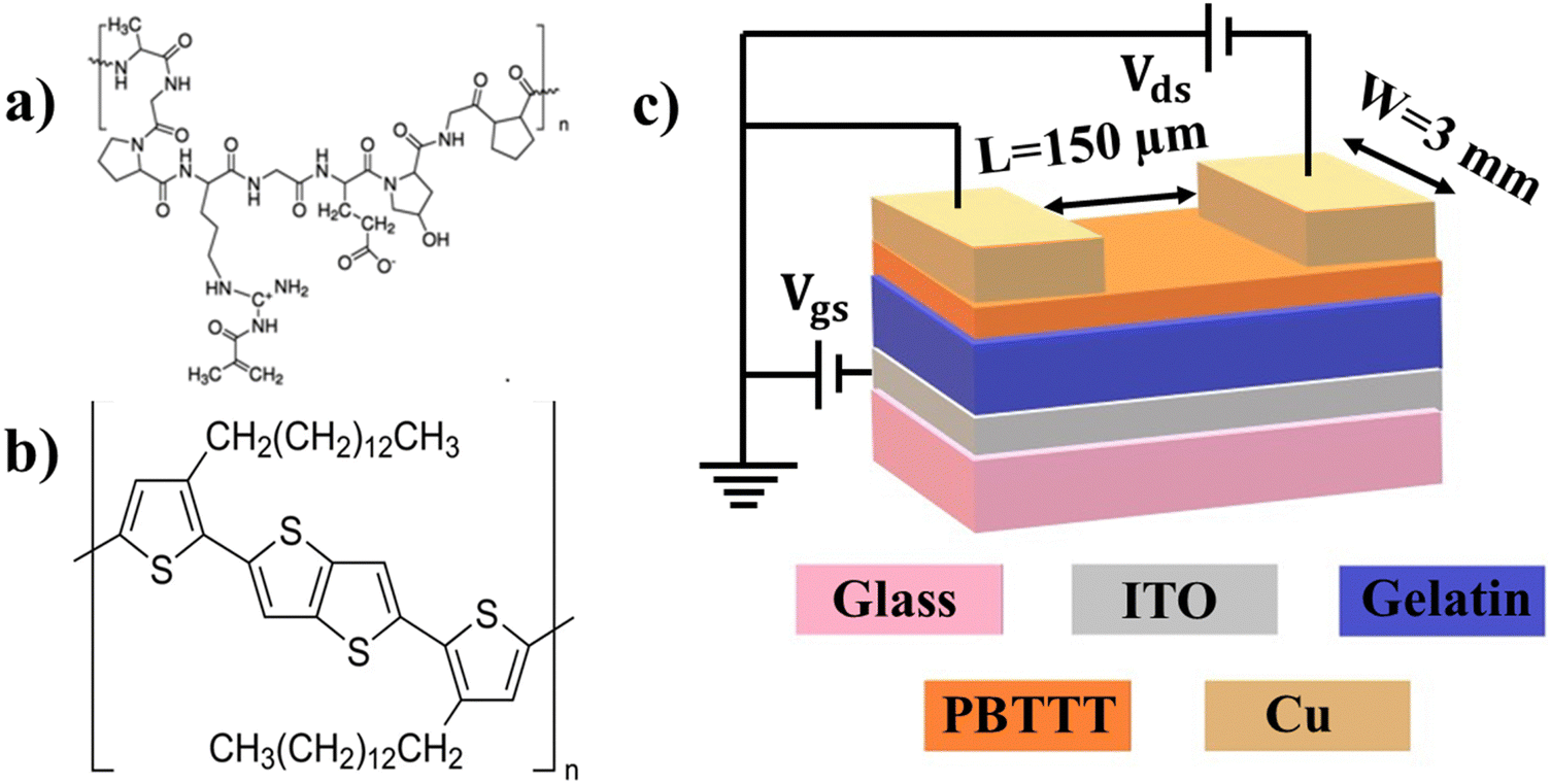 | ||
| Fig. 1 Chemical structure of (a) gelatin, (b) PBTTT-C14, and (c) schematic of gelatin-gated PBTTT-C-14-based OFET. | ||
3.1 Optical property and surface morphology of semiconducting layer
The fabrication of artificial photo synaptic OFETs for neuromorphic applications employs a device architecture and solution-processible approach that is characterized by its simplicity. Fig. 2(a) displays the UV-Vis spectrum of the PBTTT-C14 layer, which is measured to gain insight into the optical absorption of the active semiconducting channel layer of the OFETs.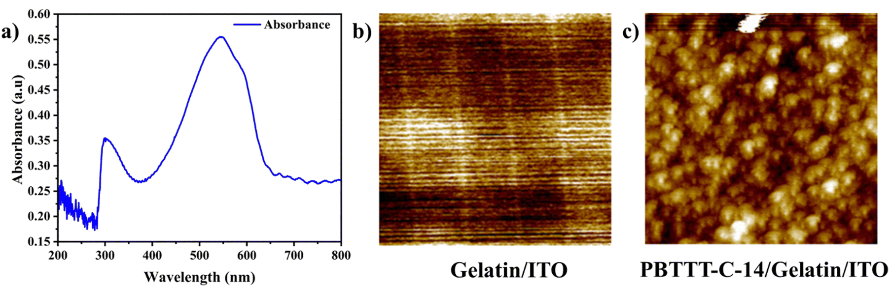 | ||
| Fig. 2 (a) UV-VIS spectra of gelatin/PBTTT-C14 layer, (b) AFM topography of a gelatin film deposited on ITO substrates (2 × 2 μm2), and (c) topography of a PBTTT-C14 film on the stack of gelatin/ITO (2 × 2 μm2). | ||
Fig. 2(a) illustrates the broad absorption band is primarily situated in the visible region with a characteristic peak centered at 545 nm.49 This infers that PBTTT-C14 is highly suitable for utilization in photo synaptic OFETs that are stimulated by visible light. In order to investigate the quality of the gelatin/ITO and PBTTT-C-14/gelatin/ITO thin film, atomic force microscopy measurements are performed, as shown in Fig. 2(b) and (c) respectively. The gelatin/ITO and PBTTT-C-14/gelatin/ITO film exhibited a reasonably smooth root mean square roughness of 0.4 nm and 1.3 nm, respectively.
3.2 The impact of light on the electrical characteristics of the OFETs
Fig. 3(a) and (b) display the output characteristics (Vds − Ids) of the synaptic OFETs under dark and illuminated conditions. The photo-response parameters of OFETs are obtained by characterizing them under white light (white LED source of intensity 2.5 mW cm−2) at the drain voltage sweep range from 0 to −20 V by keeping the gate voltage step of −2 V. Notably, the drain current of these OFETs increases under light illumination compared to dark conditions, within the same range of drain voltage sweep (0 to −20 V). The output current of the transistor is regulated by varying both the light intensity and gate voltage bias. The transfer characteristics (Vgs − Ids) are measured under both dark and illuminated conditions, as shown in Fig. 3(c) and (d), respectively. The drain current of the OFETs increases by almost three times under light compared to the current in dark conditions for the same gate voltage sweep (20 V to −20 V at Vds = −20 V). The transfer characteristics exhibit hysteresis behavior, which can be attributed to the presence of traps at the gelatin/PBTTT-C14 interface, indicating the memory-storing capability of the OFETs.10 The decrease in hysteresis behavior under light illumination conditions is due to the modulation of trap charge carriers.50 The trapped charge carriers are released under illumination conditions, causing an increase in the conductivity of the channel layer.10 The gate bias (Vgs) significantly influences the hysteresis behavior in the transfer characteristics of the OFETs. Gate bias modulates the channel conductivity in the device by accumulation/depletion of charges, which eventually affects the charge carrier transport and their trapping/de-trapping.51,52 | ||
| Fig. 3 The output characteristics of the OFETs (a) under dark, (b) under light, and transfer characteristics of the OFETs (c) under dark, (d) under light. | ||
In the hysteresis loop, under the forward sweep of the gate voltage (OFF to ON state), the trap sites at the dielectric–semiconductor interface are filled with charge carriers, resulting in a threshold voltage of −4.5 V. Conversely, when the gate voltage is swept in reverse (ON to OFF state), the trapped charge carriers are released from the traps, shifting the threshold voltage to +15 V.51 Such hysteresis behavior is controllable through the gate voltage, ultimately contributing to the memory characteristics of the OFETs.
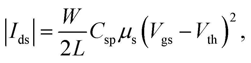
The electrical performance parameters of the gelatin-gated PBTTT-C14-based OFETs are estimated from transfer characteristics for both dark and illuminated conditions. The charge carrier mobility of the OFETs is calculated from the slope of  plot for the forward sweep of the transfer characteristics using the equation given below,
| Parameters | Under dark | Under light |
|---|---|---|
| Mobility (cm2 V−1 s−1) | 1.35 × 10⁻³ | 2.82 × 10⁻³ |
| Threshold voltage (V) | −4.5 | +7.50 |
| Sub-threshold swing (V dec−1) | 24.39 | 131.57 |
| On/off ratio | 187 | 1.53 |
The unannealed PBTTT-C14-based OFETs show the charge carrier mobility of 1.35 × 10⁻³ cm2 V−1 s−1. The mobility is comparable with the recent reports where PBTTT-C14 is utilized without any annealing.44 The OFETs exhibit a threshold voltage of −4.5 V due to the formation of EDL capacitance between the dielectric and semiconductor.44 In the gelatin dielectric, the presence of water traces interacts with acidic (and/or basic) amino acid residues, leading to the generation of mobile charges such as protons (H+) and hydroxyl ions (OH−). In the context of gelatin-gated OFETs, the introduction of negative gate voltage bias to the gate electrode helps to induce a negative surface charge which attracts mobile protons (H+) and creates an EDL at the gate electrode/dielectric interface. Simultaneously, the hydroxyl (OH−) anions were repelled and migrated towards the gelatin/semiconductor interface which forms a second EDL. Therefore, the EDL capacitance achieves which helps to get a low-voltage operation of the OFETs.44
Upon comparing the electrical parameters of the photo synaptic OFETs under dark and illuminated conditions, it is observed that there is not a significant change in charge carrier mobility. Nonetheless, it is noteworthy that the threshold voltage displayed a positive shift (+7.5 V). This phenomenon can be attributed to the charge carriers generation by the incident light, which proceeds to occupy the trap states located at the interface of gelatin and PBTTT-C14.53 Furthermore, the sub-threshold swing of the OFETs increased while the on–off ratio decreased under light illumination. This can be attributed to the modulation of channel conductivity by the photo-generated charge carriers. It is noteworthy that the photo-generated charge carriers dominate the channel conductivity over the gate effect, which is the primary reason for the observed increase in sub-threshold swing and decrease in the on–off ratio under light illumination.54 The device's drain current usually exhibits a gradual decrease over time as a result of charge trapping, which can be explained using the concept of stretched exponential variation.55,56 This phenomenon, however, can be influenced by the presence of dipoles in the dielectric layer. These dipoles can enhance the current during the polarization time by modulating the channel conductance, but eventually, the current decreases due to charge trapping. Such bias-stress effects are frequently observed in polar dielectric systems.
In the gelatin-gated PBTTT-C14-based OFETs, a slight bias-stress instability was observed, however, there was no significant change in the drain current during long-term operations. To ensure their environmental stability, we kept the devices in an ambient atmosphere to check the degradation of the devices. The devices remained stable in terms of device stability for a duration of approximately more than a month, with no decline observed in their electrical performance parameters. Despite the increased relative humidity, the devices exhibited remarkable stability under bias stress owing to the affinity of gelatin for moisture.57 The presence of even a small amount of water in the solid gelatin dielectric film can generate protons, which can readily migrate to the interface under the influence of the gate field. This phenomenon aids in the accumulation of charges in the channel.56
3.3 Photo response performance of the OFETs
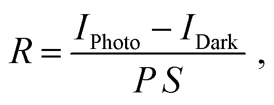
The photo response parameters (photoresponsivity, detectivity, and the ratio of photo to dark current) of the OFETs are estimated. The photoresponsivity (R), which represents the optical response capability of the OFETs, was calculated using the formulawhere, Iphoto and IDark are the photo and dark current of the OFETs, P and S represent the optical power and effective surface area of the devices respectively. Detectivity (D*), which represents the response efficiency of the OFETs under a weak light signal, was calculated using the formula,10
where, e is the electronic charge.
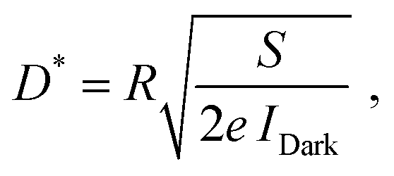
The OFETs demonstrate a relatively commendable level of photoresponsivity of 11.10 mA W−1, good detectivity of 8.55 × 10⁸ Jones, and an exceptional ratio of photo to dark current of 654.10 These photo response parameters are deemed suitable for characterizing an artificial photo synapse.
We have compared the photo response parameters of these gelatin-gated PBTTT-C14 OFETs with the relevant performance reported in the literature and summarised in Table 2. There is no report on biopolymer-gated OFETs for photo synaptic application. It is worth noting that all the OFETs (mentioned in Table 2) have SiO2 as the gate dielectric, which is different from our devices, PBTTT-C14 OFETs with gelatin as the gate dielectric. The gelatin-gated PBTTT-C14 OFETs demonstrate a simpler device architecture exhibiting photo synaptic characteristics without the incorporation of extra photosensitizing or charge-trapping elements in the devices.
| Device structure | Photosensitizer/charge trapping layer | Photo-responsivity | Detectivity | Photo and dark current ratio | Ref. |
|---|---|---|---|---|---|
| Si/SiO2/PBTTT-C14/MoO3/Ag | No | 0.01 | 3.15 × 10⁷ | 2.41 | 58 |
| Si/SiO2/OTS/PBTTT-C14/MoO3/Ag | No | 0.09 | 9.56 × 10⁷ | 11.01 | 58 |
| Si/SiO2/OTS/C60/PTCDA/SnPc/Au | Yes | 56.88 | 9.15 × 10¹² | — | 59 |
| Si/SiO2/CsPbBr3/TIPS/Au | Yes | 2 × 10³ | 2.00 × 10¹⁵ | 1.80 × 10⁵ | 60 |
| Si/SiO2/OTS/PBTTT-C14/Cu | No | 1.10 | 401 × 109 | — | 61 |
| Si/SiO2/PBTTT-C14:4CzIPN/Ti/Au | Yes | 24.00 | 1.22 × 10¹¹ | — | 62 |
| ITO/gelatin/PBTTT-C14/Cu | No | 0.01 | 8.55 × 10⁸ | 654 | This work |
3.4 Cause of the photo synaptic behavior
The operational principle of a photo synapse is primarily attributed to the interfacial charge trapping effect at the organic semiconductor/dielectric layer interface. Typically, under dark, the charge carriers become trapped at the interface between the semiconductor and dielectric materials. However, when the OFET is exposed to light, the charge carriers are stimulated and freed into the semiconducting channel. Once the light source is removed, the free-charge carriers are once again re-trapped by trap sites located at the interface. In addition to the interfacial trap, the generation of moisture-induced impurities (water and oxygen) in organic semiconductors causes oxidative trap states that also trap the charge carriers and turn out as a secondary reason for exhibiting photo synaptic behaviors. Several studies have investigated the impact of prolonged exposure to the ambient atmosphere on PBTTT-C14-based OFETs.63–65 It has been consistently observed that these OFETs undergo substantial oxidative doping over time. Consequently, the OFF current experiences a notable increase, and there is a shift towards a more positive threshold voltage. This phenomenon can be attributed to the rise in acceptor states within the bandtail. These oxidative doping states may serve as trap centers to capture the charge carriers and play a crucial role in facilitating the development of such artificial photo synapses.22 Under the influence of light irradiation, the transfer of charges happens through oxygen-induced deep traps. This process allows for the storage of photogenerated holes, which in turn enables the organic semiconductor to perform synaptic functions.66 Ruan et al. and Deng et al. provided a similar explanation for Dif-TES-ADT (organic semiconductor) based OFETs to elucidate the impact of hydrated impurities on the photo synaptic behaviors of the OFETs.22,663.5 Interfacial trap density in the OFETs
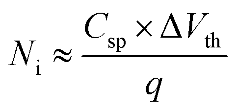
We estimated the interfacial trap density, which is determined using the transistor parameters. The sub-threshold swing method and the threshold voltage method are employed to ascertain the maximum interfacial trap density. Maximum interfacial trap density is calculated using the formula given below,67where, q, SS, Csp, KB, T are the electronic charge, sub-threshold swing, specific capacitance, Boltzmann constant, and temperature in kelvin, respectively. It gives the maximum interfacial trap density of 1.36 × 1016 cm−3. A similar order of interfacial trap density is achieved from threshold voltage using the formula67
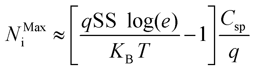
The gelatin-gated PBTTT-C14 OFETs exhibit a significantly lower interfacial trap density, approximately 102 orders of magnitude less when compared to the conventional SiO2 dielectric-based PBTTT-C14 OFETs.67 The electrical performance and photo response parameters of gelatin-based PBTTT-C14 OFETs inspire us to further characterize them for artificial synaptic applications.
3.6 Basic synaptic functionalities of the OFETs
In order to draw an analogy between the gelatin-gated PBTTT-C-14-based synaptic OFETs and neurobiological synapses, we consider optical excitation as the pre-synaptic signal and the output drain current as the post-synaptic response, as illustrated in Fig. 4. The modulation of channel conductance of the OFETs is deemed to be synaptic weight (SW), which denotes the degree of interaction between two consecutive neurons. The SW change is defined as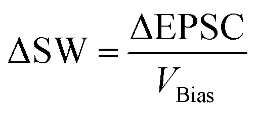 . The change in the EPSC is utilized to compute the SW modification of the OFETs, which is achieved through the regulation of input stimulation conditions, including optical pulse duration, pulse number, and pulse intensity.
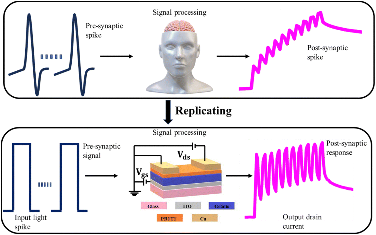 | ||
| Fig. 4 The analogy for signal processing between the human brain and artificial synaptic OFETs. | ||
The excitatory post synaptic current (EPSC) is the basic unit of the nervous system, which is related to neuroplasticity. The EPSC behavior of OFETs as shown in Fig. 5(a) is measured by triggering an optical pulse of 1 s and intensity of 0.6 mW cm−2.
 | ||
| Fig. 5 (a) EPSC response of the OFETs under the optical pulse of 1 s, (b) Charge trapping mechanism in the gelatin/PBTTT-C-14 interface, and (c) PPF behavior of the OFETs under two successive optical pulses. | ||
Upon excitation of the optical pulse with a duration of 1 s, the maximum EPSC of the OFET exhibits 17.92 nA. Following the cessation of the optical pulse, two distinct phases of decay, fast and slow, are observed prior to saturation. The synapse-like behavior is attributed to the charge-trapping effect induced by the polar group of the dielectric gelatin as illustrated in Fig. 5(b). The trapped charge carriers are subsequently released onto the semiconducting channel layer upon triggering by the optical pulse, resulting in a higher EPSC. Upon termination of the pulse, the photocurrent of the OFETs decays slowly to its initial level due to the re-trapping of the charge carriers by the trap sites. Initially, the charge carriers are trapped by the trap sites created by the polar groups of the dielectric. The introduction of photoexcitation facilitates the increment of the channel's conductivity. Upon removal of the photoexcitation, the charge carriers are once again re-trapped.
The paired-pulse facilitation (PPF) is a noteworthy neurobiological occurrence in which synaptic responses are enhanced through the application of two successive optical excitations. We measure the PPF response by triggering two consecutive optical pulses of 1s duration, separated at a pulse interval of 1 s, as depicted in Fig. 5(c). The amplitude of the EPSC for the second pulse exceeds that of the first pulse. Furthermore, the PPF index is determined through the use of the following equation,

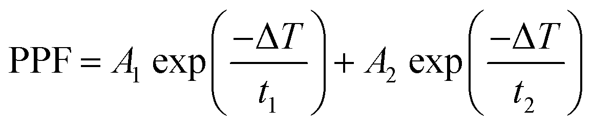
The variables A (A1, A2) and t (t1, t2) denote the initial facilitation magnitudes and relaxation time, respectively. The values t1 and t2 correspond to the rapid (1.06 s) and slow (47.32 s) decay of the PPF, respectively. The relaxation times obtained from the fitted data are consistent with the neurobiological time scale as presented in Table S2 (ESI†).10 In the field of neurobiology, PPF behavior as shown in Fig. 5(c) reflects that the synapse attempts to retain the previous stimulus even after its cessation. Specifically, following the triggering of the first optical pulse, some charge carriers remain trapped prior to the introduction of the second optical pulse, thereby causing the PPF behavior of the OFETs.
3.7 The transformation of short-term to long-term plasticity
The conversion of short-term plasticity (STP) to long-term plasticity (LTP) is a highly desirable phenomenon in neurological synapses. The transformation of short-term to long-term memory is essential for the development of long-term memory elements in artificial neural networks.68 The modulation of optical input stimulation parameters such as optical pulse duration, pulse number, and pulse intensity affect the conversion process. We measured the optical pulse duration-dependent EPSC by varying the pulse duration from 1 s to 5 s, as depicted in Fig. 6(a). These measurements demonstrate that the non-volatile flash photo memory and memory retention time increases with the increment of pulse duration, indicating the successful transformation of STP to LTP. The increase in pulse duration facilitates sufficient time for the charge carriers to release onto the conduction channel, thereby yielding a greater EPSC magnitude. The synaptic weight (SW) change upon the optical pulse durations provides a better visualization of this artificial synapse. The SW increases with the increment of the pulse duration, replicating the neurobiological synapses (ESI,† S2a)69 and it is obvious from the increment of the retention of non-volatile flash photo memory at 60 s (ESI,† S2b). Similar results have been reported in the literature.20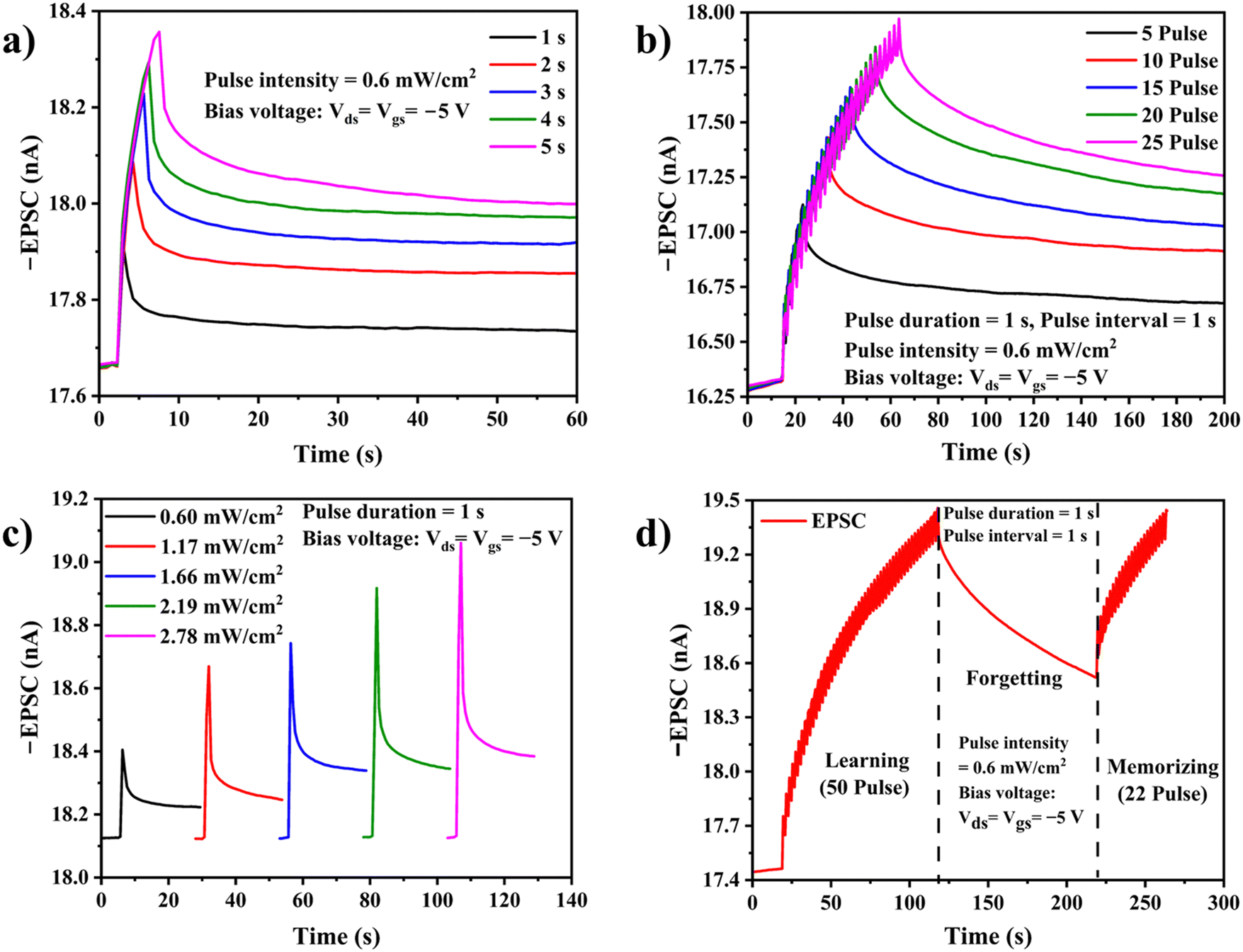 | ||
| Fig. 6 (a) Pulse duration-dependent EPSC of the OFETs, (b) pulse number-dependent EPSC of the OFETs, (c) pulse intensity-dependent EPSC of the OFETs, and (d) learning-forgetting-memorizing nature of the OFETs. | ||
Alternatively, the conversion of STP to LTP can be done by modulating the number of optical pulses. We studied EPSC dependent on pulse number by increasing the pulse number from 5 to 25, as depicted in Fig. 6(b). We noticed a transition from STP to LTP with the increment of pulse number, which is known as spike number-dependent plasticity. An increase in EPSC with pulse number, is attributed to the release of additional charge carriers following each individual optical pulse. The relationship between the non-volatile flash photo memory and optical pulse number is analyzed using an equation, 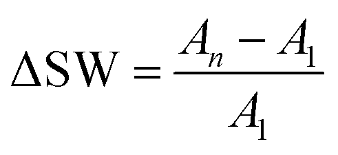 where An and A1 are the amplitude of EPSC after the nth and 1st optical pulse, respectively. The SW increases in proportion to the optical pulse numbers, as evidenced by Fig. S3a (ESI†). We analyze the photo memory retention at 200 seconds by varying pulse numbers to establish the STP to LTP conversion.
Further, converting STP to LTP is also achieved by controlling the optical pulse intensity. These OFETs have successfully replicated pulse intensity-dependent EPSC, with pulse intensity increasing from 0.6 mW cm−2 to 2.78 mW cm−2, as illustrated in Fig. 6(c). As the optical pulse intensity increases, the non-volatile flash photo memory and memory retention also increase due to the generation of more charge carriers at higher light intensities and it is obvious with photo memory retention at 25 seconds of decay, as illustrated in Fig. S4b (ESI†). Correspondingly, the SW also increases with increasing pulse intensity, which is consistent with the biological nervous system (ESI,† S4a).10
Further, we verified the learning-forgetting-memorizing nature, akin to that of the human brain, is successfully replicated in these OFETs. The human brain undergoes three primary procedures when acquiring new knowledge: learning, forgetting, and memorizing.70 Notably, the memorizing process typically requires less time than recalling forgotten information in the human brain. Similarly, in the gelatin-gated PBTTT-C14-based photo synaptic OFETs, the memorizing process requires a reduced number of optical pulses (22 pulses) compared to the learning process (50 pulses) to attain the same memory level, Fig. 6(d). These experiments establish the functioning of these OFETs performance as analogous to the human brain for learning-forgetting-memorizing characteristics. This also indicates the memory retention capabilities of the cognitive system.70
3.8 Energy consumption of the OFETs
The energy consumption per optical spike is a key feature of photo synaptic devices and realization of low energy consumption per synaptic operation is a major challenge. We estimated the energy consumption per optical event using the formula,38| Espike = Ipeak·V·t |
3.9 Logic gate implementation
The utilization of synaptic devices for the implementation of logic operations has garnered significant attention in artificial intelligence-related applications. The gelatin gated PBTTT-C14-based photo synaptic OFETs exhibit the “OR” logic operation using two optical pulses, wavelengths 440 and 620 nm, as input signals as shown in Fig. 7(a).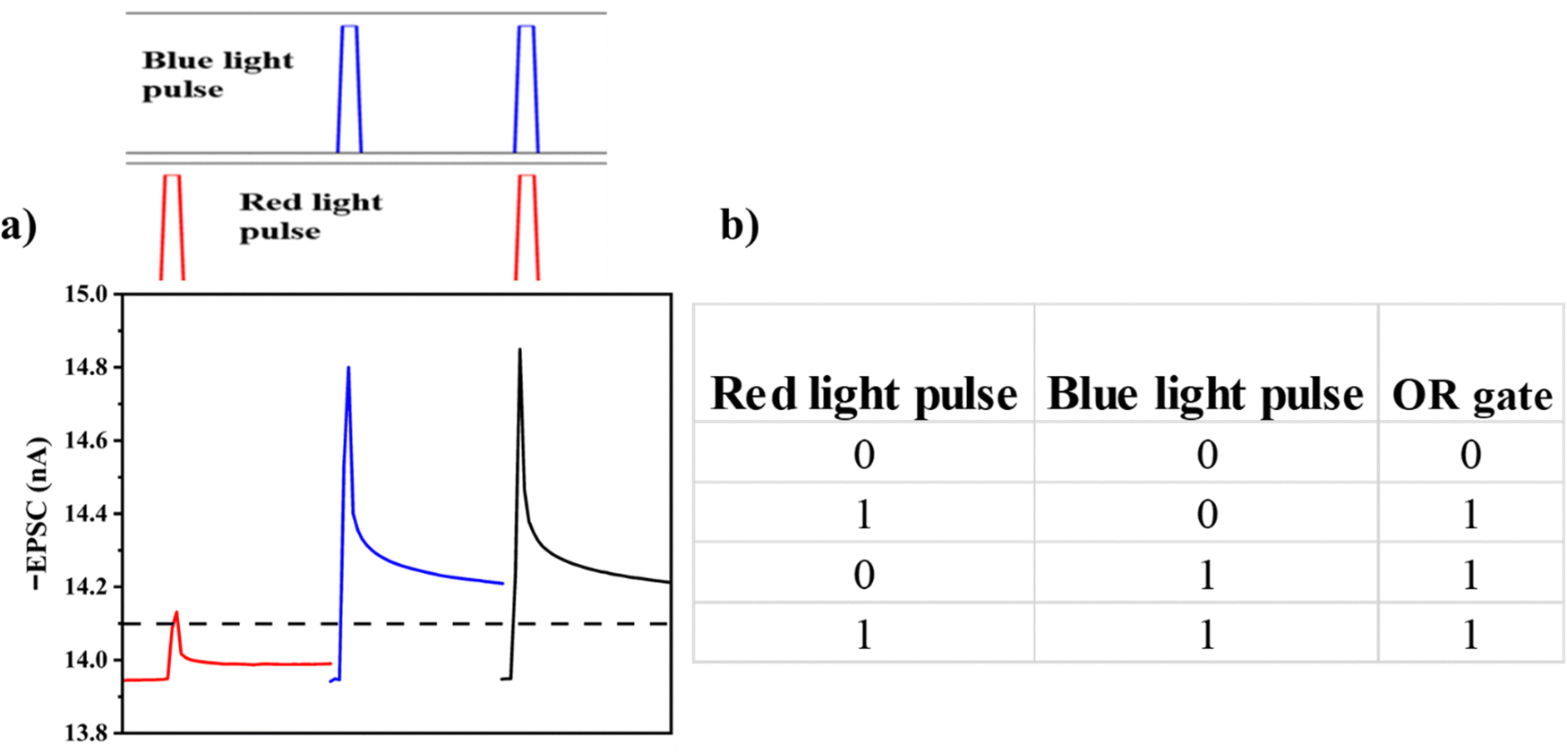 | ||
| Fig. 7 (a) Optical stimulation condition and corresponding outputs for realizing ‘OR’ gate, and (b) Truth table of ‘OR’ logic operation. | ||
The logic “1” (high) is assigned to EPSC above 14.1 nA, while below 14.1 nA are assigned the logic “0” (low). The experimental measurements for the “OR” logic operation and the corresponding outcomes are depicted in Fig. 7(a). Fig. 7(b) shows the truth table for the “OR” logic operation. In this sequence, EPSC is induced by stimulating optical pulses of two different wavelengths, with a pulse duration of 1 s, intensity of 0.6 mW cm−2, and a bias voltage of Vds = Vgs = −5 V. The amplitudes of the EPSC induced by individual optical pulses of wavelength 620 and 440 nm are 14.13 nA and 14.80 nA, respectively, both of which exceed the threshold value, resulting in an output of “1” (high). The amplitude of the EPSC when both optical pulses are on, results EPSC of 14.85 nA, also resulting in a high output. Therefore, these photo synaptic OFETs have successfully exhibited the “OR” logic operation.
3.10 Associative learning (Pavlov's dog experiment)
One of the most important features of the human brain is learning and memory through successive training which is called associative learning.71 For studying this behavior, we performed Pavlov's dog experiment using the photo synaptic OFETs. Optical pulses with two different wavelengths of 440 and 620 nm were utilized for the stimulation. The block diagram of the experimental sequence and the corresponding outputs are shown in Fig. 8(a) and (b), respectively. The photo synaptic OFETs were biased at Vds = Vgs = −5 V and the optical stimulation of 440 and 620 nm are used.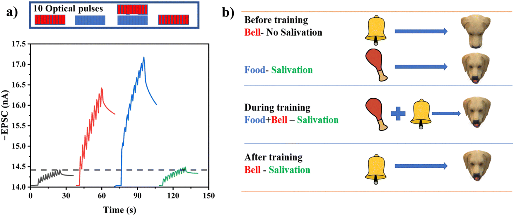 | ||
| Fig. 8 (a) Experimental sequence for realizing Pavlov's dog experiment, and (b) block diagram of Pavlov's dog experiment. | ||
To emulate Pavlov's dog experiment, we used optical pulse stimulation (10 pulses) of 620 and 440 nm as bell and food, respectively. Fig. 8(a) illustrates the EPSC of the photo synaptic OFETs triggered by different conditions of the optical pulses. Initially, the bell (620 nm) was ringing, the dog did not salivate (the maximum value of the EPSC was ∼14.42 nA, and we defined the threshold value to start salivation). However, the introduction of food (440 nm) alone resulted in salivation, the EPSC ∼16.77 nA. Subsequently, when feeding and ringing of the bell were simultaneously conducted, the dog salivated maximally, the EPSC ∼20.97 nA. After repeating this process of simultaneous feeding and ringing ten times, the dog began to salivate, the EPSC was 14.50 nA even under the introduction of bell ringing only. Therefore, the associative learning ability like the human brain, is successfully exhibited by these photo synaptic OFETs. Furthermore, we noticed the persistence of the associative learning ability after 15 minutes of the training.
3.11 Human emotion-tuneable learning and memory
The various categories of human emotions, including but not limited to happiness, neutrality, and sadness, have a significant impact on the learning and memory processes of the brain.20,72 Specifically, positive emotions, such as moments of happiness, have been shown to enhance the quality of learning and memory behavior, whereas negative emotions, such as moments of sadness, have been found to impede the brain's ability for learning and memory.73–75 This phenomenon of emotion-dependent learning and memory is successfully replicated in these photo synaptic OFETs through the examination of Vds-dependent EPSC responses. In order to investigate this emotion-tuneable learning and memory behavior, we measured the EPSC responses with varying Vds in the range of −1 V to −5 V, as illustrated in Fig. 9(a). | ||
| Fig. 9 (a) Drain voltage-dependent EPSC responses of the OFETs, (b) EPSC decay change of Vds-dependent behavior after 50 s, and (c) band bending under different Vds in PBTTT-C14. | ||
We establish a correlation between emotional states and the consolidation of learning and memory with the operating parameters of the OFETs. In this context, the drain-to-source voltage (Vds) can be likened to a parameter capable of modulating emotional states in artificial photo synaptic OFETs. Neuromodulators are essential components within the human nervous system that regulate the internal states of primary human emotions. This study has focused on the role of Vds as neuromodulators in influencing human mood.76 The EPSC response of the device is analogous to the memory behavior of the human brain in different emotional states.
The EPSC of these OFETs exhibits an increase with the rise in the Vds for the same input optical excitations. The trend of EPSC decay also indicates an improvement in memory retention behavior as noticed from the ΔEPSC after 60 s, shown in Fig. 9(b). A high Vds leads to increased band bending in PBTTT-C14 favouring the flow of more photo-generated charge carriers in the conduction channel, resulting in a higher EPSC, as shown in Fig. 9(c). Eventually, at high Vds the charge carrier recombination rate reduces, leading to a longer retention time of the photo memory.
As per the proposed analogy between the gelatin-gated PBTTT-C14-based OFETs and emotion-dependent learning and memory of the human brain, high Vds exhibit higher ΔEPSC in the OFETs. It mimics the higher memory retention behavior of the human brain in a happy emotional moment.20 Notably, an increase in EPSC changes is observed with an increase in Vds, signifying the transformation of STP to LTP. Consequently, the Vds-tunable EPSC behavior of the photo synaptic OFETs can be utilized to simulate human emotion-tunable learning and memory behavior.
3.12 Human mood influence
The influence of the colour of light on human mood, attention, consciousness, and reaction time has been established77 and it modulates brain responses during cognitive tasks.78 Notably, the impact of light of different colour has been extensively utilized in the treatment of certain mood disorders. For studying the colour of light-dependent learning responses of human brain, we performed an experiment to observe the light wavelength-dependent of EPSC in these photo synaptic OFETs. These OFETs are subjected to red, yellow, green, and blue light and their responses, as depicted in Fig. 10(a).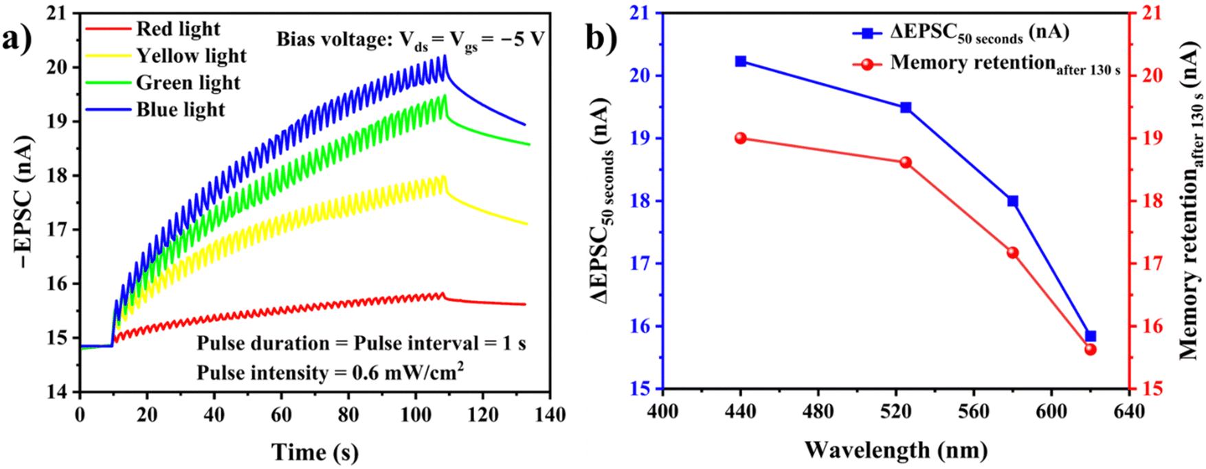 | ||
| Fig. 10 (a) Light wavelength-dependent learning responses, and (b) variation of maximum memory level and memory retention with respect to light wavelength. | ||
The EPSC responses to 50 pulses of optical stimulations increase with decreasing wavelength of light (red to blue). This observation is consistent with the response of the human brain stimulated by the different colours of light, as reported in neurobiological literature.79 The EPSC response of the OFETs depends on the excitation energy of the optical stimulation. The EPSC response is found to be highest when exposed to blue light (λ = 440 nm), which possesses the highest photon energy among all the other wavelengths (λ = 525 nm, λ = 580 nm, and λ = 620 nm) and white light used in this study.80 The optical absorption of the PBTTT-C14 active layer does not contribute to the EPSC. We attribute the wavelength-dependent EPSC behavior of the devices to the release of charge carriers from the interfacial/bulk traps under optical excitation. The research by Killgore reported that blue light stimulation results in a higher bidirectional information flow between the amygdala and dorsolateral prefrontal cortex, which is associated with an increase in positive mood. Consequently, exposure to blue light may enhance cognitive task performance and learning ability.81 These OFETs mimic the similar behavior as reported by Killgore et al.Fig. 10(b) shows the change in EPSC decay under stimulation (50 pulses) of different wavelengths of light after 130 s. To effectively demonstrate the effect of light wavelength on photo memory level and retention behavior, the maximum EPSC after 50 pulses and EPSC decay after 130 seconds are plotted against the light wavelength, as shown in Fig. 10(b). In summary, the OFETs exhibit higher memory ability at stimulation of blue light as compared to light of higher wavelengths imitating the effect of light on human learning and memory behavior.
We have compared the presented results with the recently reported biopolymer dielectric gated synaptic OFETs in Table 3. Most of the previously reported OFETs are based on either electrical signal13,82–86 or UV light signal87 as a pre-synaptic stimulus, as opposed to this investigation is based on white light as a pre-synaptic stimulus for developing artificial photo synapses.
| Device structure | Type of artificial synapse | Device performance | Applications | Ref. | ||
|---|---|---|---|---|---|---|
| Operating voltage (V) | Synaptic responses | Energy consumption (nJ) | ||||
| Si/keratin/PCDTPT/Au | Electrical synaps | −2 | EPSC, SDDP, PPF | — | Dynamic filtering | 82 |
| Si/gelatin hydrogel/IDT-BT/Au | Electrical synapse | −1 | EPSC, IPSC, PPF, PPD, STM, LTM | 0.036 | High pass filtering | 83 |
| Au/wood derive cellulose nanopaper/C8-BTBT/Au | Electrical synapse | −0.1 | EPSC, synaptic plasticity | 0.19 | Signal filtering, dendrite integration | 13 |
| Si/Au/dextran/DNTT/Au | Electrical synapse | −2 to −5 | EPSC, STP, LTP | — | — | 84 |
| Si/pectin/DNTT/Au | Electrical synapse | −0.02 | EPSC, STP, LTP, PPF | — | — | 85 |
| Glass/Au/PDPP3T/chitosan/Al | Electrical synapse | −10 | EPSC, STP, PPF | — | Dynamic tactile perception | 86 |
| Si/SiO2/silk:CDs/pentacene/Au | Opto-electronic synapse (UV light) | −1 | EPSC, STP, LTP, PPF | — | MNIST pattern recognition | 87 |
| ITO/gelatin/PBTTT-C14/Cu | Photo synaptic (white light) | −5 | EPSC, STP, LTP, PPF | 89 | Associative learning (Pavlov's dog), “OR” gate, human emotion-tunable memory | This work |
4 Conclusion
The gelatin-gated PBTTT-C14-based photo synaptic OFETs are fabricated and characterized for neuromorphic applications. The OFETs show Photoresponsivity of 11.10 mA W−1, a high Detectivity of 8.55 × 10⁸ Jones, a ratio of photo to dark current of 654. The basic neurobiological phenomena such as EPSC, PPF, STP, LTP, learning-forgetting-memorizing, and conversion of STP to LTP are successfully validated by these photo synaptic OFETs. Moreover, the ‘OR’ logic operation and associative learning experience through the emulation of Pavlov's dog experiment are demonstrated using these OFETs. More interestingly, human emotion-tuneable and mood-influencing memory and learning behavior are imitated by the gelatin-gated PBTTT-C14-based photo synaptic OFETs. The low energy consumption of ∼89 nJ per optical event makes these OFETs suitable for artificial intelligence-related applications. The gelatin-gated PBTTT-C14-based OFET exhibits encouraging characteristics which establishes it as a potential primitive element for developing artificial neural networks.Conflicts of interest
There are no conflicts to declare.Acknowledgements
B. M. and S. P. S. thank Shiv Nadar Institution of Eminence (SNIoE) and Shiv Nadar Foundation for the financial support through the doctoral fellowship.References
- Y. Cheng, H. Li, B. Liu, L. Jiang, M. Liu, H. Huang, J. Yang, J. He and J. Jiang, Vertical 0D-perovskite/2D-MoS2 van der Waals heterojunction phototransistor for emulating photoelectric-synergistically classical pavlovian conditioning and neural coding dynamics, Small, 2020, 16, 2005217 CrossRef CAS PubMed.
- R. F. Service, The brain chip, Proc. Am. Assoc. Adv. Sci., 2014, 345, 614–616 CAS.
- T. Y. Wang, J. L. Meng, Z. Y. He, L. Chen, H. Zhu, Q. Q. Sun, S. J. Ding, P. Zhou and D. W. Zhang, Room-temperature developed flexible biomemristor with ultralow switching voltage for array learning, Nanoscale, 2020, 12, 9116–9123 RSC.
- Y. Chen, W. Qiu, X. Wang, W. Liu, J. Wang, G. Dai and J. Sun, Solar-blind SnO2 nanowire photo-synapses for associative learning and coincidence detection, Nano Energy, 2019, 62, 393–400 CrossRef CAS.
- H. Tan, Z. Ni, W. Peng, S. Du, X. Liu, S. Zhao and D. Yang, Broadband optoelectronic synaptic devices based on silicon nanocrystals for neuromorphic computing, Nano Energy, 2018, 52, 422–430 CrossRef CAS.
- C. D. Danesh, C. M. Shaffer, D. Nathan, R. Shenoy, A. Tudor, M. Tadayon and Y. Chen, Synaptic resistors for concurrent inference and learning with high energy efficiency, Adv. Mater., 2019, 31, 1808032 CrossRef PubMed.
- D. Marković, A. Mizrahi, D. Querlioz and J. Grollier, Physics for neuromorphic computing, Nat. Rev. Phys., 2020, 2, 499–510 CrossRef.
- D. Kuzum, S. Yu and H. P. Wong, Synaptic electronics: materials, devices and applications, Nanotechnol., 2013, 24, 382001 CrossRef PubMed.
- Z. Lv, Y. Wang, J. Chen, J. Wang, Y. Zhou and S. T. Han, Semiconductor quantum dots for memories and neuromorphic computing systems, Chem. Rev., 2020, 120, 3941–4006 CrossRef CAS PubMed.
- L. Fang, S. Dai, Y. Zhao, D. Liu and J. Huang, Light-stimulated artificial synapses based on 2D organic field-effect transistors, Adv. Electron. Mater., 2020, 6, 1901217 CrossRef CAS.
- H. Han, H. Yu, H. Wei, J. Gong and W. Xu, Recent progress in three-terminal artificial synapses: from device to system, Small, 2019, 15, 1900695 CrossRef PubMed.
- S. Dai, X. Wu, D. Liu, Y. Chu, K. Wang, B. Yang and J. Huang, Light-stimulated synaptic devices utilizing interfacial effect of organic field-effect transistors, ACS Appl. Mater. Interfaces, 2018, 10, 21472–21480 CrossRef CAS PubMed.
- S. Dai, Y. Wang, J. Zhang, Y. Zhao, F. Xiao, D. Liu, T. Wang and J. Huang, Wood-derived nanopaper dielectrics for organic synaptic transistors, ACS Appl. Mater. Interfaces, 2018, 10, 39983–39991 CrossRef CAS PubMed.
- K. Wang, S. Dai, Y. Zhao, Y. Wang, C. Liu and J. Huang, Light-stimulated synaptic transistors fabricated by a facile solution process based on inorganic perovskite quantum dots and organic semiconductors, Small, 2019, 15, 1900010 CrossRef PubMed.
- Z. Liu, S. Dai, Y. Wang, B. Yang, D. Hao, D. Liu, Y. Zhao, L. Fang, Q. Ou, S. Jin and J. Zhao, Huang, Photoresponsive transistors based on lead-free perovskite and carbon nanotubes, Adv. Funct. Mater., 2020, 30, 1906335 CrossRef CAS.
- S. Jiang, S. Nie, Y. He, R. Liu, C. Chen and Q. Wan, Emerging synaptic devices: from two-terminal memristors to multiterminal neuromorphic transistors, Mater. Today Nano, 2019, 8, 100059 CrossRef.
- H. Han, F. Ge, M. Ma, H. Yu, H. Wei, X. Zhao, H. Yao, J. Gong, L. Qiu and W. Xu, Mixed receptors of ampa and nmda emulated using a ‘polka dot’-structured two-dimensional conjugated polymer-based artificial synapse, Nanoscale Horiz., 2020, 5, 1324–1331 RSC.
- S. Bolat, G. Torres Sevilla, A. Mancinelli, E. Gilshtein, J. Sastre, A. Cabas Vidani and Y. E. Romanyuk, Synaptic transistors with aluminum oxide dielectrics enabling full audio frequency range signal processing, Sci. Rep., 2020, 10, 1–8 CrossRef PubMed.
- H. Lee, Y. Won and J. H. Oh, Neuromorphic bioelectronics based on semiconducting polymers, J. Polym. Sci., 2022, 60, 348–376 CrossRef CAS.
- D. Liu, Q. Shi, J. Zhang, L. Tian, L. Xiong, S. Dai and J. Huang, 2D metal–organic framework based optoelectronic neuromorphic transistors for human emotion simulation and neuromorphic computing, Adv. Intell. Syst., 2022, 4, 2200164 CrossRef.
- W. Deng, Y. Lv, X. Ruan, X. Zhang, R. Jia, Y. Yu, Z. Liu, D. Wu, X. Zhang and J. Jie, Ultra-sensitive and low-power-consumption organic phototransistor enables nighttime illumination perception for bionic mesopic vision, Laser Photonics Rev., 2022, 16, 2200283 CrossRef CAS.
- W. Deng, X. Zhang, R. Jia, L. Huang, X. Zhang and J. Jie, Organic molecular crystal-based photosynaptic devices for an artificial visual-perception system, NPG Asia Mater., 2019, 11, 77 CrossRef CAS.
- Y. Wang, L. Yin, W. Huang, Y. Li, S. Huang, Y. Zhu, D. Yang and X. Pi, Optoelectronic synaptic devices for neuromorphic computing, Adv. Intell. Syst., 2021, 3, 2000099 CrossRef.
- J. Tang, F. Yuan, X. Shen, Z. Wang, M. Rao, Y. He, Y. Sun, X. Li, W. Zhang, Y. Li and B. Gao, Bridging biological and artificial neural networks with emerging neuromorphic devices: fundamentals, progress, and challenges, Adv. Mater., 2019, 31, 1902761 CrossRef CAS PubMed.
- J. Zhang, S. Dai, Y. Zhao, J. Zhang and J. Huang, Recent progress in photonic synapses for neuromorphic systems, Adv. Intell. Syst., 2020, 2, 1900136 CrossRef.
- G. Agnus, W. Zhao, V. Derycke, A. Filoramo, Y. Lhuillier, S. Lenfant, D. Vuillaume, C. Gamrat and J. P. Bourgoin, Two-terminal carbon nanotube programmable devices for adaptive architectures, Adv. Mater., 2010, 22, 702–706 CrossRef CAS PubMed.
- E. Kuramochi, K. Nozaki, A. Shinya, K. Takeda, T. Sato, S. Matsuo, H. Taniyama, H. Sumikura and M. Notomi, Large-scale integration of wavelength-addressable all-optical memories on a photonic crystal chip, Nat. Photonics, 2014, 8, 474–481 CrossRef CAS.
- J. Kim, H.-C. Lee, K.-H. Kim, M.-S. Hwang, J.-S. Park, J. M. Lee, J.-P. So, J.-H. Choi, S.-H. Kwon, C. J. Barrelet and H.-G. Park, Photon-triggered nanowire transistors, Nat. Nanotechnol., 2017, 12, 963–968 CrossRef CAS PubMed.
- D. Hao, J. Zhang, S. Dai, J. Zhang and J. Huang, Perovskite/organic semiconductor based photonic synaptic transistor for artificial visual system, ACS Appl. Mater. Interfaces, 2020, 12, 39487–39495 CrossRef CAS PubMed.
- J. Du, C. Ge, H. Riahi, E. Guo, M. He, C. Wang, G. Yang and K. Jin, Dual-gated MoS2 transistors for synaptic and programmable logic functions, Adv. Electron. Mater., 2020, 6, 1901408 CrossRef CAS.
- Y. Lee, J. Y. Oh, W. Xu, O. Kim, T. R. Kim, J. Kang, Y. Kim, D. Son, J. B. Tok, M. J. Park, Z. Bao and T. W. Lee, Stretchable organic optoelectronic sensorimotor synapse, Sci. Adv., 2018, 4, eaat7387 CrossRef CAS PubMed.
- Y. H. Chang, C. W. Ku, Y. H. Zhang, H. C. Wang and J. Y. Chen, Ultrafast responsive non-volatile flash photomemory via spatially addressable perovskite/block copolymer composite film, Adv. Funct. Mater., 2020, 30, 2000764 CrossRef CAS.
- H. T. Hsu, D. L. Yang, L. D. Wiyanto and J. Y. Chen, Red-light-stimulated photonic synapses based on nonvolatile perovskite-based photomemory, Adv. Photonics Res., 2021, 2, 2000185 CrossRef CAS.
- J. Yu, X. Yang, G. Gao, Y. Xiong, Y. Wang, J. Han, Y. Chen, H. Zhang, Q. Sun and Z. L. Wang, Bioinspired mechano-photonic artificial synapse based on graphene/MoS2 heterostructure, Sci. Adv., 2021, 7, eabd9117 CrossRef CAS PubMed.
- Q. Wu, J. Wang, J. Cao, C. Lu, G. Yang, X. Shi, X. Chuai, Y. Gong, Y. Su, Y. Zhao and N. Lu, Photoelectric plasticity in oxide thin film transistors with tunable synaptic functions, Adv. Electron. Mater., 2018, 4, 1800556 CrossRef.
- K. Wang, S. Dai, Y. Zhao, Y. Wang, C. Liu and J. Huang, Light-stimulated synaptic transistors fabricated by a facile solution process based on inorganic perovskite quantum dots and organic semiconductors, Small, 2019, 15, 1900010 CrossRef PubMed.
- B. Yang, Y. Wang, Z. Hua, J. Zhang, L. Li, D. Hao, P. Guo, L. Xiong and J. Huang, Low power consumption light-stimulated synaptic transistors based on natural carotene and organic semiconductors, Chem. Commun., 2021, 57, 8300–8303 RSC.
- G. Luo, J. Shi, W. Deng, Z. Chang, Z. Lu, Y. Zhang, R. Pan, J. Jie, X. Zhang and X. Zhang, Boosting the performance of organic photodetectors with a solution-processed integration circuit toward ubiquitous health monitoring, Adv. Mater., 2023, 35, 2301020 CrossRef CAS PubMed.
- W. Deng, H. Lei, X. Zhang, F. Sheng, J. Shi, X. Zhang, X. Liu, S. Grigorian, X. Zhang and J. Jie, Scalable growth of organic single-crystal films via an orientation filter funnel for high-performance transistors with excellent uniformity, Adv. Mater., 2022, 34, 2109818 CrossRef CAS PubMed.
- L.-K. Mao, J.-C. Hwang, T.-H. Chang, C.-Y. Hsieh, L.-S. Tsai, Y.-L. Chueh, S. S. H. Hsu, P.-C. Lyu and T.-J. Liu, Pentacene organic thin-film transistors with solution-based gelatin dielectric, Org. Electron., 2013, 14, 1170–1176 CrossRef CAS.
- C. Lee, Y. Chang, L. Wang and Y. Wang, Biodegradable materials for organic field-effect transistors on a paper substrate, IEEE Electron Device Lett., 2019, 40, 236–239 CAS.
- Y. He, J. Sun, C. Qian, L. A. Kong, J. Jiang, J. Yang, H. Li and Y. Gao, Solution-processed natural gelatin was used as a gate dielectric for the fabrication of oxide field-effect transistors, Org. Electron., 2016, 38, 357–361 CrossRef CAS.
- H. Yuan, X. Wang, B. Lian, H. Zhang, X. Fang, B. Shen, G. Xu, Y. Xu, S. C. Zhang, H. Y. Hwang and Y. Cui, Generation and electric control of spin–valley-coupled circular photogalvanic current in WSe2, Nat. Nanotechnol., 2014, 9, 851–857 CrossRef CAS PubMed.
- M. R. Kiran, Y. Yadav and S. P. Singh, Threshold voltage tuning in gelatin biopolymer-gated high-performance organic field-effect transistors, Synth. Met., 2023, 297, 117398 CrossRef CAS.
- R. S. Duman, G. K. Aghajanian, G. Sanacora and J. H. Krystal, Synaptic plasticity and depression: new insights from stress and rapid-acting antidepressants, Nat. Med., 2016, 22, 238–249 CrossRef CAS PubMed.
- G. Neves, S. F. Cooke and T. V. Bliss, Synaptic plasticity, memory and the hippocampus: a neural network approach to causality, Nat. Rev. Neurosci., 2008, 9, 65–75 CrossRef CAS PubMed.
- R. S. Duman, Synaptic plasticity and mood disorders, Mol. Psychiatry, 2002, 7, S29–S34 CrossRef CAS PubMed.
- K. Kim, C. L. Chen, Q. Truong, A. M. Shen and Y. Chen, A carbon nanotube synapse with dynamic logic and learning, Adv. Mater., 2013, 25, 1693–1698 CrossRef CAS PubMed.
- A. K. Singh, A. Pandey and P. Chakrabarti, Fabrication, modelling and characterization of green light photosensitive p-channel-Poly [2,5-bis (3-tetradecylthiophen-2-yl) thieno [3,2-b] thiophene] organic semiconductor based phototransistors, Org. Electron., 2019, 75, 105424 CrossRef CAS.
- D. K. Hwang, M. S. Oh, J. M. Hwang, J. H. Kim and S. Im, Hysteresis mechanisms of pentacene thin-film transistors with polymer/oxide bilayer gate dielectrics, Appl. Phys. Lett., 2008, 92, 013304 CrossRef.
- M. Egginger, S. Bauer, R. Schwödiauer, H. Neugebauer and N. S. Sariciftci, Current versus gate voltage hysteresis in organic field effect transistors, Monatsh. Chem., 2009, 140, 735–750 CrossRef CAS.
- S. P. Singh, A. Sellinger and A. Dodabalapur, Electron transport in copper phthalocyanines, J. Appl. Phys., 2010, 107, 044509 CrossRef.
- M. C. Hamilton, S. Martin and J. Kanicki, Effect of illumination on organic polymer thin-film transistors, Mater. Res. Soc. Symp. Proc., 2003, 771 Search PubMed.
- J. L. Brédas, J. P. Calbert, D. A. da Silva Filho and J. Cornil, Organic semiconductors: A theoretical characterization of the basic parameters governing charge transport, Proc. Natl. Acad. Sci. U. S. A., 2002, 99, 5804–5809 CrossRef PubMed.
- S. Mandal, A. Mandal, G. Jana, S. Mallik, S. Roy, A. Ghosh, P. K. Chattaraj and D. K. Goswami, Low operating voltage organic field-effect transistors with gelatin as a moisture-induced ionic dielectric layer: the issues of high carrier mobility, ACS Appl. Mater. Interfaces, 2020, 12, 19727–19736 CrossRef CAS PubMed.
- N. V. Subbarao, M. Gedda, P. K. Iyer and D. K. Goswami, Enhanced environmental stability induced by effective polarization of a polar dielectric layer in a trilayer dielectric system of organic field-effect transistors: a quantitative study, ACS Appl. Mater. Interfaces, 2015, 7, 1915–1924 CrossRef CAS PubMed.
- G. Konwar, P. Saxena, V. Raghuwanshi, S. Rahi and S. P. Tiwari, Low-voltage flexible organic transistors based on a water-soluble natural gate dielectric exhibiting high-performance and stability, Flexible Printed Electron., 2022, 7, 025004 CrossRef CAS.
- B. Mandal, P. Sonar and S. P. Singh, Visible light-stimulated artificial synapse based on an organic field-effect transistor for imitating human emotions and mood swings, ACS Appl. Electron. Mater., 2024, 6(4), 2420–2433 CrossRef CAS.
- F. Huang, X. Wang, K. Xu, Y. Liang, Y. Peng and G. Liu, Broadband organic phototransistor with high photoresponse from ultraviolet to near-infrared realized via synergistic effect of trilayer heterostructure, J. Mater. Chem. C, 2018, 6, 8804–8811 RSC.
- J. Liu, Z. Yang, Z. Gong, Z. Shen, Y. Ye, B. Yang, Y. Qiu, B. Ye, L. Xu, T. Guo and S. Xu, Weak light-stimulated synaptic hybrid phototransistors based on islandlike perovskite films prepared by spin coating, ACS Appl. Mater. Interfaces, 2021, 13, 13362–13371 CrossRef CAS PubMed.
- B. Mandal, S. Kumar and S. P. Singh, Detection of principal and higher harmonic frequencies using stochastic resonance phenomenon in PBTTT-C14-based organic field-effect transistor, Appl. Phys. Lett., 2024, 124, 103507 CrossRef CAS.
- M. A. Iqbal, X. Weng, C. Kang, N. Arif, K. Wu, W. Tang, S. Dai, X. Fang, H. Cai and Y. J. Zeng, Thermally activated delayed fluorescence triplet state excitons for high-performance organic photodetectors: a novel strategy, Laser Photonics Rev., 2024, 18, 2300612 CrossRef CAS.
- I. McCulloch, M. Heeney, M. L. Chabinyc, D. DeLongchamp, R. J. Kline, M. Cölle, W. Duffy, D. Fischer, D. Gundlach, B. Hamadani and R. Hamilton, Semiconducting thienothiophene copolymers: design, synthesis, morphology, and performance in thin-film organic transistors, Adv. Mater., 2009, 21, 1091–1109 CrossRef CAS.
- I. McCulloch, M. Heeney, C. Bailey, K. Genevicius, I. MacDonald, M. Shkunov, D. Sparrowe, S. Tierney, R. Wagner, W. Zhang and M. L. Chabinyc, Liquid-crystalline semiconducting polymers with high charge-carrier mobility, Nat. Mater., 2006, 5, 328–333 CrossRef CAS PubMed.
- Y. Li, Y. Wu, P. Liu, M. Birau, H. Pan and B. S. Ong, Poly (2, 5-bis (2-thienyl)-3, 6-dialkylthieno [3,2-b] thiophene) s—high-Mobility semiconductors for thin-film transistors, Adv. Mater., 2006, 18, 3029–3032 CrossRef CAS.
- X. Ruan, S. Cheng, W. Deng, Y. Tan, Z. Lu, J. Shi, X. Zhang and J. Jie, Insights into the origins of minority carrier traps in solution-processed organic semiconductors and their effects on transistor photostability, Adv. Electron. Mater., 2022, 8, 2200355 CrossRef CAS.
- Y. Yadav and S. P. Singh, Effect of dielectric surface passivation on organic field-effect transistors: spectral analysis of the density of trap-states, Semicond. Sci. Technol., 2021, 37, 015015 CrossRef.
- D. Norris, Short-term memory and long-term memory are still different, Psychol. Bull., 2017, 143, 992 Search PubMed.
- N. Du, X. Zhao, Z. Chen, B. Choubey, M. Di Ventra, I. Skorupa, D. Bürger and H. Schmidt, Synaptic plasticity in memristive artificial synapses and their robustness against noisy inputs, Front. Neurosci., 2021, 15, 660894 Search PubMed.
- R. L. Davis and Y. Zhong, The biology of forgetting—a perspective, Neuron, 2017, 95, 490–503 CrossRef CAS PubMed.
- W. A. Suzuki, Associative learning signals in the brain, Prog. Brain Res., 2008, 169, 305–320 Search PubMed.
- C. M. Tyng, H. U. Amin, M. N. Saad and A. S. Malik, The influences of emotion on learning and memory, Front. Psychol., 2017, 1454 CrossRef PubMed.
- I. Boniwell and A. D. Tunariu, EBOOK: Positive psychology: Theory, research and applications, McGraw-Hill Education, UK, 2019 Search PubMed.
- E. M. Selhub and A. C. Logan, Your brain on nature: The science of nature's influence on your health, happiness and vitality, John Wiley & Sons, 2012 Search PubMed.
- L. Li, A. D. I. Gow and J. Zhou, The role of positive emotions in education: a neuroscience perspective, Mind Brain Educ., 2020, 14, 220–234 CrossRef.
- S. Gu, F. Wang, N. P. Patel, J. A. Bourgeois and J. H. Huang, A Model for Basic Emotions Using Observations of Behavior in Drosophila, Front. Psychol., 2019, 10, 781 CrossRef PubMed.
- S. W. Lockley, E. E. Evans, F. A. Scheer, G. C. Brainard, C. A. Czeisler and D. Aeschbach, Short-wavelength sensitivity for the direct effects of light on alertness, vigilance, and the waking electroencephalogram in humans, Sleep, 2006, 29, 161–168 Search PubMed.
- R. Golmohammadi, H. Yousefi, N. S. Khotbesara, A. Nasrolahi and N. Kurd, Effects of light on attention and reaction time: A systematic review, J. Health Sci. Res., 2021, 21, e00529 CrossRef PubMed.
- L. K. Grant, B. A. Kent, M. D. Mayer, R. Stickgold, S. W. Lockley and S. A. Rahman, Daytime exposure to short wavelength-enriched light improves cognitive performance in sleep-restricted college-aged adults, Front. Neurol., 2021, 12, 624217 CrossRef PubMed.
- X. Wang, S. Yang, Z. Qin, B. Hu, L. Bu and G. Lu, Enhanced multiwavelength response of flexible synaptic transistors for human sunburned skin simulation and neuromorphic computation, Adv. Mater., 2023, 35, 2303699 CrossRef CAS PubMed.
- A. Alkozei, N. S. Dailey, S. Bajaj, J. R. Vanuk, A. C. Raikes and W. D. Killgore, Exposure to blue wavelength light is associated with increases in bidirectional amygdalaDLPFC connectivity at rest, Front. Neurol., 2021, 12, 625443 CrossRef PubMed.
- J. Ko, L. T. Nguyen, A. Surendran, B. Y. Tan, K. W. Ng and W. L. Leong, Human hair keratin for biocompatible flexible and transient electronic devices, ACS Appl. Mater. Interfaces, 2017, 9, 43004–43012 CrossRef CAS PubMed.
- D. Lai, E. Li, Y. Yan, Y. Liu, J. Zhong, D. Lv, Y. Ke, H. Chen and T. Guo, Gelatin-hydrogel based organic synaptic transistor, Org. Electron., 2019, 75, 105409 CrossRef CAS.
- Y. Yang, X. Zhao, S. Wang, C. Zhang, H. Sun, F. Xu, Y. Tong, Q. Tang and Y. Liu, Exploration of the proton conduction behavior in natural neutral polysaccharides for biodegradable organic synaptic transistors, J. Mater. Chem. C, 2020, 8, 16542–16550 RSC.
- Y. Li, C. Zhang, X. Zhao, Y. Tong, Q. Tang and Y. Liu, Ultrasensitive and degradable ultraflexible synaptic transistors based on natural pectin, ACS Appl. Electron. Mater., 2021, 4, 316–325 CrossRef.
- Y. Zang, H. Shen, D. Huang, C. A. Di and D. Zhu, A dual-organic-transistor-based tactile-perception system with signal-processing functionality, Adv. Mater., 2017, 29, 1606088 CrossRef PubMed.
- Z. Lv, M. Chen, F. Qian, V. A. Roy, W. Ye, D. She, Y. Wang, Z. X. Xu, Y. Zhou and S. T. Han, Mimicking neuroplasticity in a hybrid biopolymer transistor by dual modes modulation, Adv. Funct. Mater., 2019, 29, 1902374 CrossRef.
Footnote |
| † Electronic supplementary information (ESI) available. See DOI: https://doi.org/10.1039/d4ma00209a |
| This journal is © The Royal Society of Chemistry 2024 |