
 Open Access Article
 This Open Access Article is licensed under a
 Creative Commons Attribution 3.0 Unported Licence
Ultrathin nanoporous metallic films and their integration in sensors†
Hyunah
Kwon
 *ab,
Mariana
Alarcón-Correa
ab,
Izar
Schärf
a and
Peer
Fischer
abcd
*ab,
Mariana
Alarcón-Correa
ab,
Izar
Schärf
a and
Peer
Fischer
abcd
aInstitute for Molecular Systems Engineering and Advanced Materials, Heidelberg University, INF 225, 69120 Heidelberg, Germany. E-mail: hyunah.kwon@mr.mpg.de
bMax Planck Institute for Medical Research, Jahnstrasse 29, 69120 Heidelberg, Germany
cCenter for Nanomedicine, Institute for Basic Science (IBS), Seoul 03722, Republic of Korea
dDepartment of Nano Biomedical Engineering (NanoBME), Advanced Science Institute, Yonsei University, Seoul, 03722, Republic of Korea
First published on 28th March 2024
Abstract
Nanoporous metallic films (NPMFs), featuring an extensive surface area and a network of interconnected ligaments, are making a significant impact across various fields due to their unique physical and chemical properties, which are distinct from those of dense films. We fabricate ultrathin NPMFs that have a thickness of one ligament diameter (tens of nm) and introduce a facile method to transfer these films onto an alternative substrate, including nanostructured sensing materials. The method is simple and applicable to a wide spectrum of nanoporous metallic films. Unlike other methods, we can grow ultrapure films with a large number of metals and metal compositions. We apply our growth and transfer method to enhance the sensor performance of a metal oxide gas sensor. By transferring a NPMF onto Pt we increase the sensitivity and also reduce the required operating temperatures. Further, we describe how ultrathin nanoporous films composed of reactive and alloyed metals can be obtained, and thereby indicate how ultrathin, yet highly robust, NPMFs show promise for catalytic applications and sensors.
Introduction
Nanoporous metallic films (NPMFs) exhibit unique properties distinct from dense metal films.1,2 NPMFs feature a network of pores and ligaments, providing them with exceptional optical,3 electrical,4 chemical,5 and mechanical properties.6 Their large surface-area-to-volume ratios, combined with a high density of surface atoms on curved surfaces, give rise to significant catalytic activities that are absent in dense films.7,8 Such properties have gained significant attention for roles in applications in fields like energy conversion,9 sensing,10 and as plasmonic materials.11 Moreover, NPMFs are not only conductive due to their interconnected structure but can also achieve optical transparency at minimal thicknesses,12 making them promising candidates for transparent conducting films.Dealloying is the most prevalent method used to obtain NPMFs.13 This process involves the selective chemical etching of one or more less noble metals from an alloy.13 However, dealloying faces considerable challenges, particularly when forming NPMFs with non-noble or reactive metals.13,14 It requires carefully selected combinations of materials and chemistries to ensure the selective etching of non-desired metals in the master alloy.14 Consequently, generalizing fabrication conditions, which typically use wet processes, is challenging,14 often leading to undesirable impurities from secondary metals in the final porous film.15 Additionally, creating ultra-thin films with a thickness comparable to a ligament diameter, a characteristic which is critical for a number of applications, proves challenging in any wet synthesis method.16
Our group has recently introduced a novel dry synthesis approach,17,18 addressing these challenges. This method is based on physical vapor deposition and low-temperature plasma treatment and eliminates the need for solution processing or harsh chemicals. This approach offers additional benefits of reducing both material and processing costs by eliminating the need to remove sacrificial metal elements. Our method is versatile and one of its advantages is that it can be used with any number of metals and their compositions. Leveraging these benefits, we herein show how these ultrathin films can, despite their thickness of less than 20 nm, be handled and transferred, such that they can integrated with existing sensor technologies and device architectures. We show that the NPMFs films maintain their conductivity after transfer and that even cm-sized films can be handled without collapsing the film.
Our work also includes the demonstration of a catalytic overlayer that can be applied to gas sensing materials. Metals serve as catalysts to enhance the performance of gas sensors. Notably, Pt nanoparticles, when integrated into nanostructured metal oxides, such as SnO2, have demonstrated significant catalytic improvements for various gases while also lowering the operating temperature.19–21 The functionalization of sensing materials with catalysts has been achieved predominantly through chemical synthesis or physical vapor deposition of metals. Herein, we introduce the transfer of a Pt NPMF onto a SnO2 layer, which improves the sensitivity and which lowers the operating temperatures. Unlike traditional methods where metals are incorporated within the sensing materials, the nanoporous Pt film is applied as a catalytic overlayer on top of the sensor device. Therefore, our NPMF transfer technique is versatile, offering a straightforward application to any sensor device type, thereby facilitating the efficient fabrication of diverse sensor arrays without the need to separately optimize individual sensing materials. Furthermore, our NPMFs can be formed from reactive metals and alloyed metals, which potentially display interesting catalytic properties.
Experimental details
Fabrication and transfer of Au and Pt NPMFs
The Au and Pt NPMFs are fabricated as follows. Poly(methyl methacrylate) (PMMA, average Mw ∼ 120![[thin space (1/6-em)]](https://www.rsc.org/images/entities/char_2009.gif) 000 g mol−1 from Sigma-Aldrich) was dissolved (1.5 wt% or 5 wt%) in chloroform for more than 12 hours at room temperature by magnetic stirring. The solution was spin-coated on a Si wafer (boron-doped, 〈100〉 orientation) at 1000 rpm for 1 min. Au (>99.999% purity) and Pt (>99.99% purity) was evaporated by e-beam on the PMMA film at room temperature with an oblique angle of 80°, at a rate of 0.05 nm s−1, a target thickness of 10 nm considering the tooling factor, and a rotation speed of 0.72° s−1. The NPMF films were plasma treated (see ESI,† Table S1). To transfer these films, a water-soluble sacrificial layer was introduced prior to PMMA spin-coating. Two different materials were used for the fabrication of the sacrificial layer. The first one is NaCl (>99.5% from Carl Roth), which was e-beam evaporated at a rate of 0.4 nm s−1 to a thickness of 300 nm, before the addition of the PMMA followed by evaporation of the metals on the double layer. The sample was floated on Milli-Q water until the NPMF naturally separated from the Si substrate. The other is PVA (Mowiol 4–88, average Mw ∼ 31000 g mol−1 from Sigma-Aldrich), which was prepared as a 1 wt% solution by stirring it at 20 °C for 5 hours. Following this, 1 mL of the mixture was centrifuged at 17900 rcf in 1.5 mL Eppendorf tubes. From this, 800 μL of the supernatant was carefully transferred using a pipette into a new tube. This was then spin-coated at 5000 rpm for 60 s. The sample was slowly immersed at an oblique angle into the Milli-Q water, until the NPMF layer floated on the water surface. A sapphire ([0001]-plane, double-side polished, >99.99% purity) or alternately the SnO2 gas sensor device was immersed to transfer the floating NPMF on the substrate/sensor. Any remaining water after transfer was completely dried with air. The sample was then immersed in acetone to completely remove any potential PMMA residues.
000 g mol−1 from Sigma-Aldrich) was dissolved (1.5 wt% or 5 wt%) in chloroform for more than 12 hours at room temperature by magnetic stirring. The solution was spin-coated on a Si wafer (boron-doped, 〈100〉 orientation) at 1000 rpm for 1 min. Au (>99.999% purity) and Pt (>99.99% purity) was evaporated by e-beam on the PMMA film at room temperature with an oblique angle of 80°, at a rate of 0.05 nm s−1, a target thickness of 10 nm considering the tooling factor, and a rotation speed of 0.72° s−1. The NPMF films were plasma treated (see ESI,† Table S1). To transfer these films, a water-soluble sacrificial layer was introduced prior to PMMA spin-coating. Two different materials were used for the fabrication of the sacrificial layer. The first one is NaCl (>99.5% from Carl Roth), which was e-beam evaporated at a rate of 0.4 nm s−1 to a thickness of 300 nm, before the addition of the PMMA followed by evaporation of the metals on the double layer. The sample was floated on Milli-Q water until the NPMF naturally separated from the Si substrate. The other is PVA (Mowiol 4–88, average Mw ∼ 31000 g mol−1 from Sigma-Aldrich), which was prepared as a 1 wt% solution by stirring it at 20 °C for 5 hours. Following this, 1 mL of the mixture was centrifuged at 17900 rcf in 1.5 mL Eppendorf tubes. From this, 800 μL of the supernatant was carefully transferred using a pipette into a new tube. This was then spin-coated at 5000 rpm for 60 s. The sample was slowly immersed at an oblique angle into the Milli-Q water, until the NPMF layer floated on the water surface. A sapphire ([0001]-plane, double-side polished, >99.99% purity) or alternately the SnO2 gas sensor device was immersed to transfer the floating NPMF on the substrate/sensor. Any remaining water after transfer was completely dried with air. The sample was then immersed in acetone to completely remove any potential PMMA residues.
Fabrication of the gas sensor device
A Si wafer that is coated with 300 nm SiO2 was patterned using photolithography to create an interdigitated electrode (IDE) array. Ti (20 nm) and Pt (150 nm) were deposited by e-beam evaporation to form an IDE. The substrate was patterned again for the sensing layer. SnO2 (99.9%, Sigma Aldrich) slanted nanorods were deposited using (glancing angle vapor deposition (GLAD) – a form of shadow physical vapor deposition)22 at 80° with a target thickness of 200 nm, a rate of 0.25 nm s−1.Sheet resistance measurement
A four-point probe station (Ossila) was used to measure the sheet resistance of the Au NPMF transferred onto a sapphire substrate. The separation between probes was 1.27 mm.Sensing measurement
We used a compact chamber probe measurement setup from Nextron Co. The chamber contained a temperature-controlled heating stage and ports for the gas inlet and outlet. The temperature was controlled in the range from room temperature to 300 °C with a PID system. The temperature was increased by steps of 50 °C. Gas flow was precisely controlled using mass flow controllers (GE50A from MKS Instruments), with dry air serving as the balance gas. The gas was introduced into the chamber at a pressure of 1 atm. The total gas flow into the chamber was maintained at 500 sccm. All current measurements were taken at 0.1 V. Prior to the initial gas exposure at each operating temperature, the sample was purged with air for 20 minutes to stabilize the current level.Fabrication of NPMF with reactive metals and alloys
Different PMMA solutions were used for each NPMF – 1.5 wt%, 2.5 wt%, and 5 wt%. All metals were e-beam deposited at 80° with target thicknesses of 10 nm. For alloyed metals, each metal was co-deposited (50:50) each at 0.25 nm s−1. The sample was then plasma treated (for further details of the fabrication conditions, see ESI,† Table S1).
Transmission electron microscopy (TEM)
For the preparation of samples for TEM analysis, the PMMA film was partially etched leaving a thin PMMA layer under the NPMFs, and the sample was immersed in pure acetone to dissolve the PMMA film to yield a free-standing NPMF that could be detached. The NPMF was then picked up with a plasma-cleaned TEM copper grid, and subsequently dried under an Ar flow for an hour. A ZEISS SESAM (sub-electronvolt-sub-angstrom-microscope) with a field emission gun (200 kV), equipped with a monochromator, a MANDOLINE-filter, and a 60 mm2 Thermo Fischer ultradry EDX detector, was used to obtain the TEM-EDX data.Results and discussion
The fabrication of NPMF through a dry synthesis method that we proposed earlier involves several key steps.17,18 Initially, a layer of PMMA is spin-coated to act as a sacrificial layer. Following this, a layer of metal nanoparticles is deposited via glancing angle deposition. The sample then undergoes plasma treatment, which not only etches away the PMMA layer but also facilitates the formation of interconnected NPMF structures from metal nanoparticles with a thickness corresponding to their ligament diameter. To enable the transfer of this ultra-thin NPMF, a water-soluble layer is introduced beneath the PMMA layer, as depicted in Fig. 1. We employed two different materials for this layer – spin-coated PVA or a deposited layer of NaCl. The dry synthesis procedure is replicated on top of this water-soluble layer.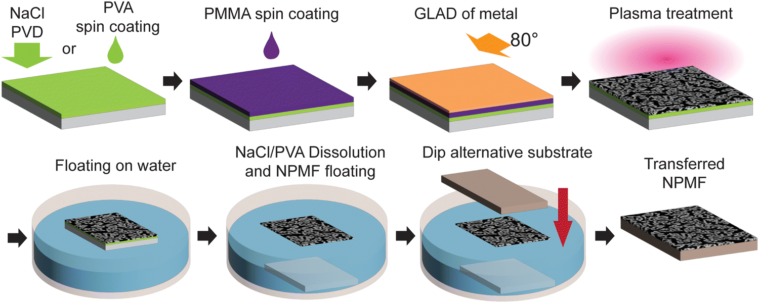 | ||
| Fig. 1 Schematic showing the dry synthesis of a nanoporous metallic film (NPMF) and the transfer method. Water-soluble PVA or NaCl layer was spin-coated or e-beam deposited on a wafer, respectively, followed by spin-coating of a PMMA sacrificial layer. A thin layer of Au nanoparticles was deposited with GLAD at 80°, and the sample was plasma-treated to form a nanoporous mesh structure. The PMMA layer was etched by the plasma. The sample was then placed on water where the NPMF detached as the NaCl layer slowly dissolved in water, leaving the NPMF floating on the water surface. Another substrate was then used to pick up the nanoporous metallic film on it. | ||
A transfer method using water surface tension was reported before.23 Once the synthesis is complete, the sample is carefully placed on the water surface. Due to the water surface tension, the sample remains afloat. Over time, the water gradually dissolves the PVA or the NaCl layer, causing the NPMF to detach from the substrate. Here, the water surface tension keeps the ultrathin NPMF afloat on the water surface without the need for a solid support. Remerkably, despite its high porosity and its ultra-thin nature – with a thickness of about 20 nm, the NPMF maintains its structural interconnectivity on water, a proof of the stabilizing effect of the water's surface tension. The floating NPMF can then be transferred onto a new substrate and/or device architecture. This is achieved by carefully immersing the new substrate into the water, approaching the floating NPMF from above and then lifting it. The NPMF thereby adheres to the substrate's surface and ultimately strongly binds due to van der Waals forces. Fig. 2(a) and (b) provide optical images of the NPMF floating after the NaCl and PVA layers have dissolved, respectively. For a detailed visual representation of the dissolution process at × 6.6 speed, refer to ESI,† Video S1. The NPMFs maintain their robust structure on the water surface, and connected films with sizes ranging from mm to cm can thus be obtained.
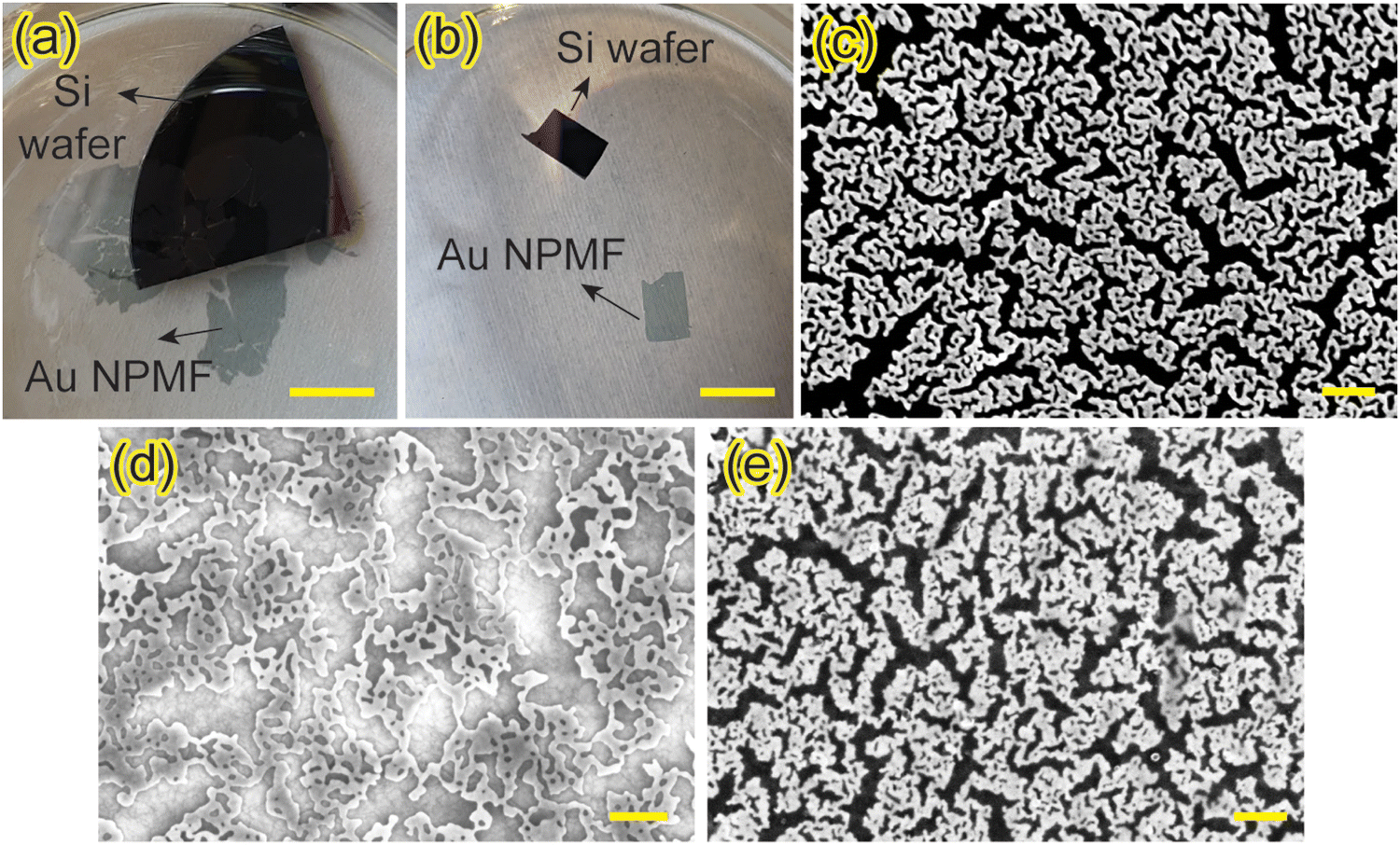 | ||
| Fig. 2 Optical images of a floating Au NPMF on top of water after dissolving (a) NaCl, and (b) PVA. Scale bars for (a) and (b) are 10 mm. (c) SEM image of the original Au NPMF after plasma treatment. (d) SEM image of transferred Au NPMF onto a sapphire substrate by dissolving NaCl. (e) SEM image of transferred Au NPMF onto a glass slide by dissolving PVA. Scale bars for (c)–(e) are 200 nm. | ||
The SEM image of the original Au NPMF is shown in Fig. 2(c). Post-plasma treatment for 5 minutes, the Au nanoparticles exhibit a robust interconnected structure, with the ligament diameters averaging around 20 nm. Subsequently, this NPMF was transferred onto an electrically insulating sapphire substrate to evaluate its conductivity post-transfer. Fig. 2(d) and (e) show the NPMF post-transfer, now adhering to the sapphire (after dissolving NaCl) and a glass substrate (after dissolving PVA), respectively. Importantly, the NPMF retains its intricate interconnected nanosturcutre, and the pores remain distinct and well-defined, with no signs of aggregation, even after the transfer. To assess the conductivity of the transferred NPMF, a 4-probe measurement was conducted. The results reveal an average resistance of 95.2 Ω sq−1. This level of conductivity indicates that the transferred NPMF also holds potential for application as transparent conducting electrodes.
The NPMFs are not only promising in electrical applications but also show great promise as catalysts. Specifically, Pt nanoparticles are often employed as catalysts in gas sensing applications. To see the capability of Pt NPMF as a catalyst for gas sensing properties, a Pt NPMF was initially grown on a NaCl layer (Fig. 3(a)), and then successfully transferred onto a nanostructured SnO2 sensing layer (Fig. 3(b)). The transfer was effective with the Pt NPMF uniformly overlaying the SnO2 layer, as confirmed by energy dispersive X-ray mapping analyses (ESI,† Fig. S1). The sample was then thermal annealed at 350 °C for an hour. The device image is shown in ESI,† Fig. S2. The Pt NPMF was stable even after annealing at 500 °C for 2 hours in ambient air, which is higher than typical operating temperature of metal oxides gas sensors (see ESI,† Fig. S3).
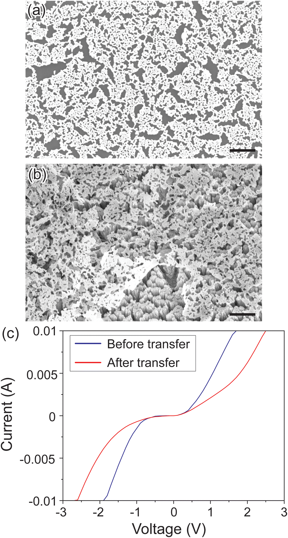 | ||
| Fig. 3 (a) SEM image of Pt NPMF. (b) The Pt NPMF was transferred on the SnO2 nanostructures which is the gas sensing material deposited on IDEs. Sample was annealed at 350 °C for an hour. Scale bar: 500 nm. (c) I–V characteristics of the SnO2-based sensor device before (blue) and after (red) NPMF transfer. | ||
The electrical characteristics of the resulting SnO2-based sensor device are depicted in Fig. 3(c). The current–voltage (I–V) curve suggests a light back-to-back Schottky-type behaviour, attributed to the Schottky barrier formed at the Pt/SnO2 interface between the electrodes and the sensing layer. Notably, post-transfer of the Pt NPMF onto the SnO2, there was a decrease in the current level. This reduction is ascribed to the diminished electron concentration in the SnO2, a consequence of the depletion layer formed at the interface between Pt NPMF and the SnO2.
Gas sensing measurements were conducted on two devices to evaluate the catalytic effects of Pt NPMF and their role in enhancing the sensing properties. Fig. 4(a)–(e) illustrates the H2 sensing results obtained at varying operating temperatures ranging from 100–300 °C, in increments of 50 °C, and at different H2 concentrations ranging from 100–500 ppm, in increments of 100 ppm, with and without NPMF. The measurement process involved alternating between two minutes of gas exposure and two minutes of air purging, with each concentration being tested twice. To clearly visualize the current variations before and after each gas exposure, the baseline current was subtracted from the original current measurements.
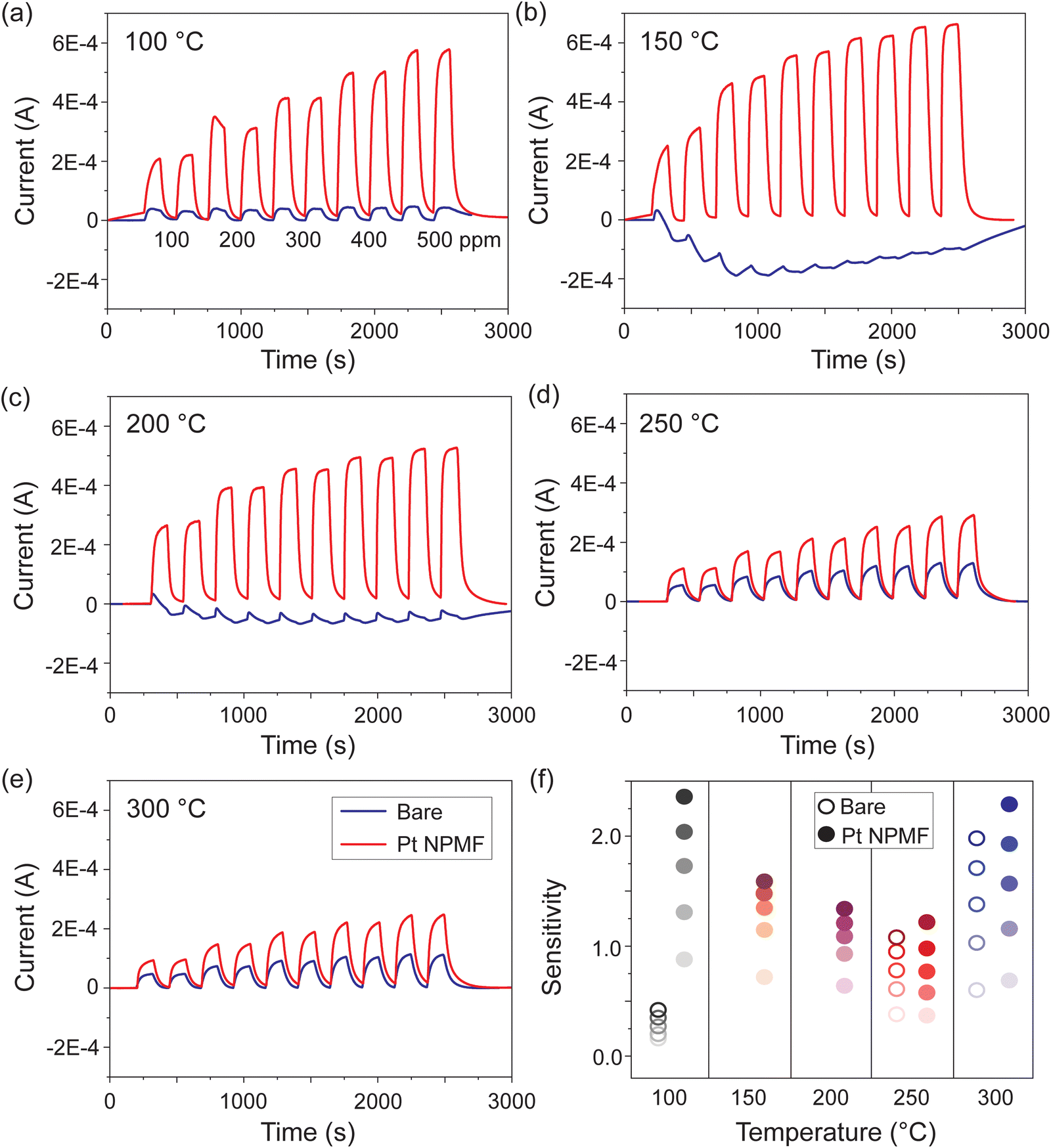 | ||
| Fig. 4 Concentration-dependent H2 sensing measurement results at a voltage of 0.1 V. Sensor operating temperatures are (a) 100, (b) 150, (c) 200, (d) 250, and (e) 300 °C. H2 100, 200, 300, 400, and 500 ppm were exposed in series, each twice. Blue lines are for the bare, and red lines are for Pt NPMF transferred sensor device. H2 exposure and dry air purging were repeated for 2 minutes each. Baseline of the current was subtracted from the original data to visualize the current difference during H2 exposure. (f) Concentration and temperature dependent H2 sensitivity. Empty circles are for the bare, and full-filled circles are for the Pt NPMF transferred device. Colors change from light to dark as the concentration increases. Sensitivity for the bare device at 150 and 200 °C was not plotted, as the sensor response was not clear. | ||
It was observed that the device with the transferred Pt NPMF exhibited a significantly larger current variation, which is particularly noticeable at lower operating temperatures. While the device without Pt NPMF (bare device) showed a negligible response to H2 at 150 °C and 200 °C, the device with Pt NPMF demonstrated a pronounced response, achieving a saturated and stable current level within 2 minutes. The response of the bare device enhanced with increasing operating temperature, whereas the Pt NPMF device exhibited optimal performance at lower temperatures.
The sensitivity of the device was calculated by (Igas − Iair)/Iair. The calculated sensitivities are summarized in Fig. 4. The sensitivity results for the bare device at 150 °C and 200 °C were removed due to their negligible response. The color intensity in the graph correlates with the concentration. Overall, the Pt NPMF device demonstrated superior sensitivity and a clear dependence on concentration, across the spectrum of operating temperatures. Especially, the sensitivity at lower temperatures showed a dramatic enhancement. Sensitivity values obtained with the same device, but a month after the initial experiments, display similar results, particularly at lower temperature and lower concentrations, as shown in ESI,† Fig. S4. The observed saturation at higher temperatures is attributed to degraded SnO2 nanostructures that were exposed to humid air at ambient conditions. Importantly, the Pt NPMF remained robust as shown in ESI,† Fig. S5. These results imply the effectiveness of Pt NPMF in reducing the operating temperature of the SnO2-based gas sensor, paving the way for low-temperature H2-sensing applications.
In addition to H2, other gases including CO and acetone were also tested to evaluate the catalytic performance of Pt NPMF on gas sensing properties, and the sensitivities were obtained in the same manner. Fig. 5(a)–(c) presents a comparative analysis of the sensitivity of the bare and the Pt NPMF device for 500 ppm concentrations of H2, CO, and acetone. For H2, the Pt NPMF device shows its highest sensitivity of 2.36, observed at 100 °C, whereas the bare device reached its peak performance only at the highest temperature of 300 °C, with a sensitivity of 1.98 for 500 ppm H2. In the case of CO, the Pt NPMF device recorded its highest sensitivity at 1.24 at 150 °C, while the bare device recorded 1.41 at 300 °C. These results suggest that the Pt NPMF overlayer contributes significantly to lowering the operating temperature, which is required for effective H2 and CO gas sensing. For acetone, both exhibited an increase in sensitivity with rising temperature. Nevertheless, the Pt NPMF device consistently outperformed the bare device across all temperatures, with a sensitivity of 17.45 at 300 °C, indicating also an overall enhancement in sensitivity.
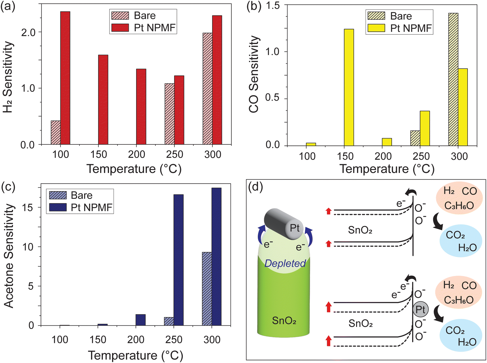 | ||
| Fig. 5 Sensitivity as a function of the operating temperature and role of Pt NPMF: (a) H2, (b) CO, and (c) Acetone sensitivity for the bare device (striped) and Pt NPMF transferred device (filled). Pt NPMF transferred device clearly shows enhanced sensitivity for three gases, especially at lower temperature. (d) Sensing mechanism comparison for SnO2 nanostructures with (bottom) and without (top) Pt NPMF coating. Top: Electron concentration in SnO2 increases upon gas exposure as gases donate electrons through chemical reactions. Bottom: Pt NPMF enhances electron depletion via the Schottky effect and catalyzes additional electron donation upon gas exposure, significantly affecting electron concentration modulation in SnO2. | ||
Fig. 5(d) shows the potential sensing mechanism in our devices. Initially, the SnO2 surface is covered by ionosorbed oxygen species, creating a depletion region. Upon exposure to gas molecules, these oxygen species react with the gases to form CO2, H2O, and release electrons. These electrons are then introduced in the SnO2, increasing its electron concentration and consequently, the current during gas exposure. The presence of Pt NPMF intensifies the depletion effect at the top of the SnO2, not only by catalytically supporting the ionosorption of the oxygen species, but also forming a Schottky barrier at the interface between SnO2 and Pt. Consequently, when the gas molecules interact with the Pt NPMF-coated SnO2, the additional depletion layer facilitates a notable shift in electron concentrations. The Pt NPMF also catalytically enhances the overall sensing properties, contributing to a lowering of the operating temperature. Moreover, the highly porous nature of the Pt NPMF allows for efficient gas diffusion into and out of the SnO2 nanostructured layers. Its ultrathin nature ensures that the Pt NPMF overlayer does not impede the response or recovery times.
In addition to Pt, a broad spectrum of metals can serve as catalysts to enhance gas sensing.23–25 The specific affinity of various metals towards specific gas molecules offers opportunities to increase both the sensitivity and selectivity of gas sensors. By fabricating a diverse range of NPMFs, we can tailor sensors to not only detect gases with superior performance but also distinguish between various gas species with improved selectivity.
Our dry synthesis approach is versatile and applicable for a wide array of metals, including non-noble and reactive metals, as well as alloys composed of more than two metal elements. Fig. 6(a)–(f) shows a collection SEM images of NPMFs, all fabricated using this dry synthesis method. They include reactive metals like Mg (6a) and Al (6b), alloyed metals such as NiFe (6c) AuAg (6d), AuPt (6e), and PtPd (6f). All of these NPMFs feature ligaments on the scale of tens of nanometers, and exhibit a cohesive interconnected structure.
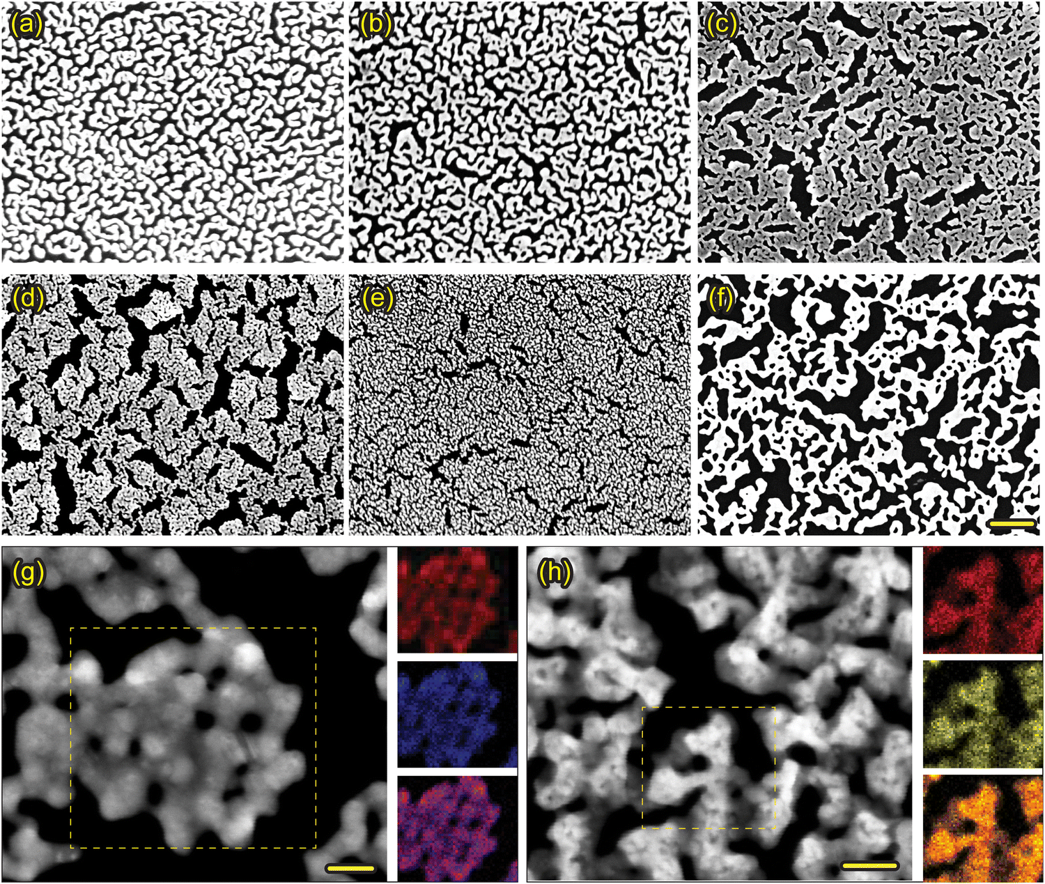 | ||
| Fig. 6 SEM images of (a) Mg, (b) Al, (c) NiFe, (d) AuAg, (e) AuPt, and (f) PtPd NPMFs. Scale bar is 500 nm. TEM images and TEM-EDX analyses of a selected regions of (g) AuAg NPMF, and (h) AuPt NPMF. Both scale bars are 20 nm. EDX analysis results are displayed on the right – the first and second images are from single element signals, while the third image are combined signals. The Au, Ag, and Pt signals are indicated in red, blue, and yellow, respectively. Each element is uniformly distributed throughout the NPMFs. | ||
For the AuAg, and AuPt NPMFs, we also performed a TEM analysis, as shown in Fig. 6(g) and (h), respectively. These exhibit ligaments approximately 10 nm in size, all forming an interconnected network. TEM-EDX analyses were conducted on selected regions marked by yellow dashed boxes. The first and second images on the right represent signals from individual elements, while the third image combines these signals. The signals for Au, Ag, and Pt are color-coded in red, blue, and yellow, respectively. Both NPMFs demonstrate a uniform distribution of each element throughout the structure. These films can serve as catalytic overlayers for gas sensors. Given the unique catalytic characteristics of different metals or their alloys,24–26 varying the catalytic overlayer can enhance the gas selectivity of sensor devices.
Conclusions
Ultrathin NPMFs have been successfully fabricated through a dry synthesis route, introducing a novel method for transferring them onto alternative substrates. Traditional techniques for creating NPMFs often lack the versatility to form ultrathin films and to do so with a spectrum of metals (see ESI,† Table S2). In contrast, our dry synthesis approach enables the fabrication of ultrathin NPMFs from a large array of metals. Remarkably, the thickness of these films corresponds merely to the diameter of the ligaments, forming a monolayer network of pores and ligaments with thicknesses ranging from 10 to 50 nm, which was determined by TEM analysis in our previous work.17,18 As we show, these films can be effectively transferred to alternative substrates by utilizing the surface tension of water. Employing water-soluble PVA and NaCl as sacrificial layers allows the ultrathin NPMFs to float on water without collapsing, facilitating their transfer. The electrical conductivity of the NPMFs was confirmed through 4-probe measurements, with probe distances of 1.27 mm, indicating that the structures remain fully interconnected across several mm to cm. Our dry synthesis method for creating ultrathin NPMFs combined with our effective transfer technique, can also be used to form transparent conducting films.Furthermore, the integration of our NPMFs as catalytic overlayers significantly enhances the gas sensing performance and reduces the operating temperature. The application of a catalytic overlayer also facilitates the selective detection of specific gases through catalytic filtering of interfering substances, as is supported by related studies.24,27 Our NPMF fabrication method has been extended to include not only noble but also non-noble, reactive metals, and alloys, broadening the scope for incorporating various metals with unique catalytic properties. This expansion is highly promising for the enhanced gas selectivity in sensor arrays, which is crucial for demanding applications in fields ranging from environmental monitoring to the detection of explosives.
Author contributions
HK and PF conceptualized the project. HK, MA, and IS carried out experiments and analyzed results. All authors wrote, contributed to, and discussed the final manuscript.Conflicts of interest
There are no conflicts to declare.Acknowledgements
The authors would like to express their gratitude to P. van Aken for access to the Stuttgart Center for Electron Microscopy and K. Hahn for supporting TEM-EDX measurements. Open Access funding provided by the Max Planck Society.References
- B. C. Tappan, S. A. Steiner III and E. P. Luther, Angew. Chem., Int. Ed., 2010, 49, 4544–4565 CrossRef CAS PubMed.
- R. Ron, D. Gachet, K. Rechav and A. Salomon, Adv. Mater., 2017, 29, 1604018 CrossRef PubMed.
- A. N. Koya, X. Zhu, N. Ohannesian, A. A. Yanik, R. P. Alabastri, R. Proietti Zaccaria, W.-C. Krahne, D. Shih and D. Garoli, ACS Nano, 2021, 15, 6038–6060 CrossRef CAS PubMed.
- R. Zhang and H. Olin, Materials, 2014, 7, 3834–3854 CrossRef PubMed.
- T. Jin, M. Terada, M. Bao and Y. Yamamoto, ChemSusChem, 2019, 12, 2936–2954 CrossRef CAS PubMed.
- S. Shi, Y. Li, B.-N. Ngo-Dinh, J. Markmann and J. Weissmüller, Science, 2021, 371, 1026–1033 CrossRef CAS PubMed.
- A. R. Silva Olaya, B. Zandersons and G. Wittstock, ChemElectroChem, 2020, 7, 3670–3678 CrossRef CAS.
- X. Lu, T. Yu, H. Wang, L. Qian and P. Lei, ACS Catal., 2020, 10, 8860–8869 CrossRef CAS.
- Q. Chen, Y. Ding and M. Chen, MRS Bull., 2018, 43, 43–48 CrossRef CAS.
- H.-J. Qiu, X. Li, H.-T. Xu, H.-J. Zhang and Y. Wang, J. Mater. Chem. C, 2014, 2, 9788–9799 RSC.
- S. Kwon, M. J. Oh, S. Lee, G. Lee, I. Jung, M. Oh and S. Park, J. Am. Chem. Soc., 2023, 145, 27397–27406 CrossRef CAS PubMed.
- K. Hiekel, S. Jungblut, M. Georgi and A. Eychmüller, Angew. Chem., Int. Ed., 2020, 59, 12048–12054 CrossRef CAS PubMed.
- G. Wittstock, M. Bäumer, W. Dononelli, T. Klüner, L. Lührs, C. Mahr, L. V. Moskaleva, M. Oezaslan, T. Risse, A. Rosenauer, A. Staubitz, J. Weissmülle and A. Wittstock, Chem. Rev., 2023, 123, 6716–6792 CrossRef CAS PubMed.
- X. Guo, C. Zhang, Q. Tian and D. Yu, Mater. Today Commun., 2021, 26, 102007 CrossRef CAS.
- A. Lackmann, M. Bäumer, G. Wittstock and A. Wittstock, Nanoscale, 2018, 10, 17166–17173 RSC.
- G. Benetti, F. Banfi, E. Cavaliere and L. Gavioli, Nanomaterials, 2021, 11, 3116 CrossRef CAS PubMed.
- H. Kwon, H.-N. Barad, A. R. Silva Olaya, M. Alarcón-Correa, K. Hahn, G. Richter, G. Wittstock and P. Fischer, ACS Appl. Mater. Interfaces, 2023, 15, 5620–5627 CrossRef CAS PubMed.
- H. Kwon, H.-N. Barad, A. R. Silva Olaya, M. Alarcón-Correa, K. Hahn, G. Richter, G. Wittstock and P. Fischer, ACS Catal., 2023, 13, 11656–11665 CrossRef CAS.
- B. Lin, F. Jia, B. Lv, Z. Qin, P. Liu and Y. Chen, Mater. Res. Bull., 2018, 106, 403–408 CrossRef CAS.
- Q. Zhou, L. Xu, A. Umar, W. Chen and R. Kumar, Sens. Actuators, B, 2018, 256, 656–664 CrossRef CAS.
- L. Chen, Y. Song, W. Liu, H. Dong, D. Wang, J. Liu, Q. Liu and X. Chen, J. Alloys Compd., 2022, 893, 162322 CrossRef CAS.
- M. Kang, I. Cho, J. Park, J. Jeong, K. Lee, B. Lee, D. Del Orbe Henriquez, K. Yoon and I. Park, ACS Sens., 2022, 7, 430–440 CrossRef CAS PubMed.
- B. Le Borgne, S. Liu, X. Morvan, S. Crand, R. A. Sporea, N. Lu and M. Harnois, Adv. Mater. Technol., 2019, 4, 1800600 CrossRef.
- Y. K. Moon, S.-Y. Jeong, Y. C. Kang and J.-H. Lee, ACS Appl. Mater. Interfaces, 2019, 11, 32169–32177 CrossRef CAS PubMed.
- J. M. Baik, M. Zielke, M. H. Kim, K. L. Turner, A. M. Wodtke and M. Moskovits, ACS Nano, 2010, 4, 3117–3122 CrossRef CAS PubMed.
- S. Jaballah, Y. Alaskar, I. AlShunaifi, I. Ghiloufi, G. Neri, C. Bouzidi, H. Dahman and L. El Mir, Chemosensors, 2021, 9, 300 CrossRef CAS.
- S.-Y. Jeong, Y. K. Moon, J. Wang and J.-H. Lee, Nat. Commun., 2023, 14, 233 CrossRef CAS PubMed.
Footnote |
| † Electronic supplementary information (ESI) available: The NPMF fabrication method, SEM-EDX results, the optical image of the sensor device, stability, the table of comparison of various techniques to fabricate NPMFs, and a video showing the transfer of the film. See DOI: https://doi.org/10.1039/d4ma00134f |
| This journal is © The Royal Society of Chemistry 2024 |