DOI:
10.1039/D4MA00095A
(Paper)
Mater. Adv., 2024,
5, 5998-6006
Thermoelectric characterization of crystalline nano-patterned silicon membranes†
Received
31st January 2024
, Accepted 2nd June 2024
First published on 4th June 2024
Abstract
Research towards efficient and environmentally friendly thermoelectrics proposes silicon nanostructures as possible candidates through reduction of the phononic thermal conductivity. However, there is scarce literature about experimental measurements of the thermoelectric figure-of-merit zT on actual crystalline silicon devices. This article reports on the fabrication and full thermoelectric characterization of crystalline 60 nm thick membranes. To that end, an experiment with four types of built-in devices was designed using a silicon-on-insulator substrate to extract the Seebeck coefficient, electrical conductivity and thermal conductivity. The results show indeed a reduced thermal conductivity of 31 W m−1 K−1 for a 60 nm thick Si membrane and κ = 18 W m−1 K−1 for a porous Si membrane. This reflects an 88% reduction in thermal conductivity compared to the bulk Si material and a 42% reduction compared to plain Si membranes. In terms of power generation, the power factor of the fabricated devices surpasses that of state-of-the-art silicon thin films at room temperature. Notably, a zT figure of merit of 0.04 is reported for a 60 nm thick phonon-engineered Si membrane, which is considerably higher than that of bulk Si(0.001) but lower than previously reported results on other types of nano-objects.
Introduction
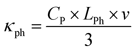
In the field of thermoelectricity, silicon nanostructures have emerged as promising alternatives to conventional thermoelectric materials (e.g., Bi, Sb, Te, and Pb alloys) due to silicon's abundance, non-toxic nature, and compatibility with CMOS technology.1–9 However, silicon's inefficiency as a thermoelectric material stems from its high thermal conductivity of 150 W m−1 K−1,10 in contrast to bismuth telluride alloys with a thermal conductivity approximately one hundred times lower (∼1.5 W m−1 K−1).11 The dimensionless figure of merit (zT), a crucial metric for thermoelectric efficiency, is approximately 1 for Bi2Te3 at room temperature12 and drops below 0.001 for bulk silicon.13 At temperature T, zT is defined aswhere S, σ, and κ denote the Seebeck coefficient, electrical conductivity, and thermal conductivity, respectively. The thermal conductivity is expressed as the sum of two components: lattice or phononic thermal conductivity (κPh), and electronic thermal conductivity (κe). The latter one is owing to heat transfer by free charge carriers through the structure. The phononic contribution, evaluated in the diffusive regime, is expressed as| |  | (2) |
where κPh is the lattice thermal conductivity related to the heat propagation through the lattice vibrations (phonons) depending on mean free path LPh, sound velocity v and specific heat CP.
The literature reports methods to enhance the thermoelectric figure of merit (zT) for silicon by increasing the ratio of electrical conductivity to thermal conductivity (σ/κ). This involves diminishing thermal conductivity (κ) by minimizing the impact of phonon-mediated heat transport (κPh), a dominant factor in semiconductors.14 The reduction of κPh can be accomplished by diminishing the mean free path of phonons through diffusion via artificial defects and boundaries. This approach can be achieved by employing nanometric structures like thin membranes15–22 or nanowires (NW),23–25 surface roughening,26,27 surface oxidization,28,29 and so-called phonon engineering methods.30–38 Arguably, some of the reported synthesis methods, such as nanosphere lithography, or objects, such as nanowires, are unlikely to be transferred into a mass production infrastructure.
The characterization of such nanostructures involves additional complexity compared to bulk measurements. Especially, heat flux evaluation is delicate since many parasitic leakage channels are involved and non-negligible at the nanoscale. Furthermore, the fabrication processes sometimes involve aggressive etching steps that can deteriorate the crystallinity of samples. This work aims at tackling the lack of experimental measurements for the thermoelectric figure of merit (zT) in crystalline silicon nanostructures assembled in CMOS compatible devices.
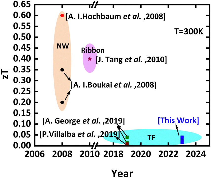
In this study, we focus on the fabrication and characterization of devices designed to assess thermoelectric (TE) properties, including the thermal conductivity, Seebeck coefficient, and electrical conductivity of crystalline silicon membranes. Our investigation involves both plain (P) and phononic engineered (PE) silicon membranes, integrated into a planar configuration on the same chip. A novel Seebeck measurement method employing a thermometry technique is introduced. The subsequent section details the fabrication process and characterization methodology, presenting the power factor (PF) and zT for both P and PE membranes. A comparative analysis is provided, highlighting the comparison with the state of the art (Fig. 1).
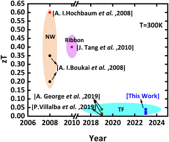 |
| | Fig. 1 Reported values of zT for crystalline nanostructure silicon planar configurations. | |
Fabrication and characterization
Design and fabrication
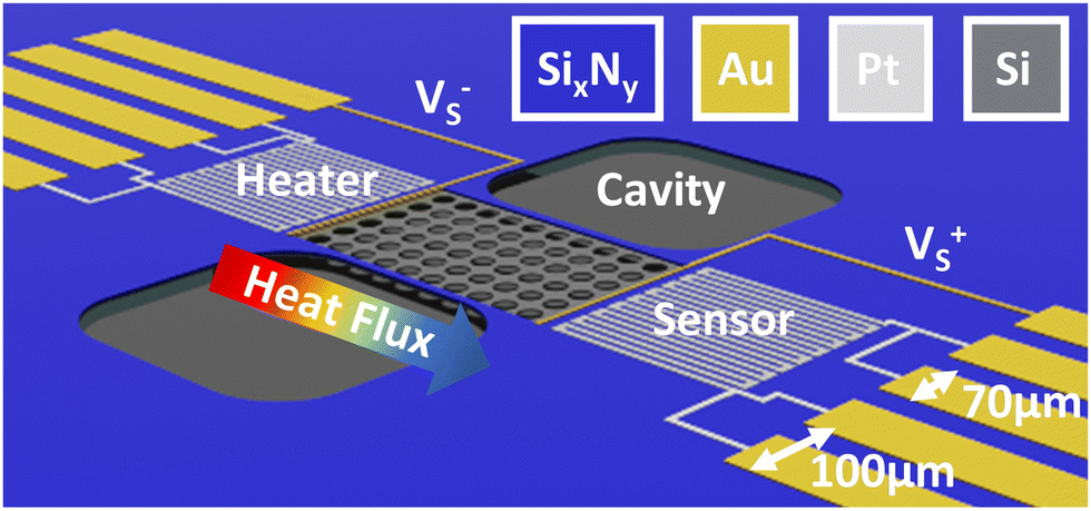
The Seebeck coefficient is a critical parameter for evaluating the efficiency of a thermoelectric material. To measure the Seebeck coefficient of silicon (Si) we designed a suspended micro-thermoelectric membrane schemed on Fig. 2. The technique employs resistive thermometry to measure the temperature difference along the Si membrane. Two serpentine platinum wires are used either as Joule heaters or resistive sensors. They are positioned near the edges of the membrane to ensure precise measurement of the temperature difference. The crystalline silicon membrane is fully suspended and is connected at both ends with gold metallic pads. These contact enable the measurement of Seebeck voltage resulting from temperature gradients.
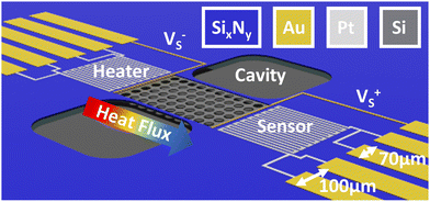 |
| | Fig. 2 Seebeck coefficient measurement device. | |
The devices are made from silicon on insulator (SOI) substrates using processes compatible with the complementary metal–oxide–semiconductor (CMOS) technology, as depicted in Fig. 3. The process builds upon prior efforts aimed at reducing the thermal conductivity of silicon through a combination of silicon thinning and the creation of pore lattices.1,31,39 The starting point is an SOI wafer featuring a 70 nm thick active layer, a 145 nm thick buried oxide (BOX) layer and a 745 μm silicon handler. (a) High-resolution e-beam lithography and Cl2/Ar reactive ion etching (RIE) are then employed to define the pore patterns (b), creating a square lattice of 46 nm diameter pores with a pitch of 100 nm, as illustrated in Fig. 4(d). The selection of these dimensions represents a compromise between technological constraints, minimizing pitch and neck size, and enhancing porosity. This approach aims at maximising the impact of pores towards lower thermal conductivity.40,41 Subsequently, the silicon is doped using either p-boron or n-phosphorus ion implantation, targeting a concentration of 1019 cm−3 (c). Then, a low-stress non-stoichiometric silicon nitride layer (SixNy) is deposited (d) isolating the membrane from the central platinum resistive heater. Silicon nitride serves the dual purpose of insulating the membrane electrically and enhancing the mechanical robustness of the structures. Cavities are then etched around the membranes to create apertures for subsequent suspension (e). SixNy is removed from the silicon membranes to facilitate the flow of electric current while preventing the formation of a parallel thermal conduction channel in silicon nitride (SixNy).
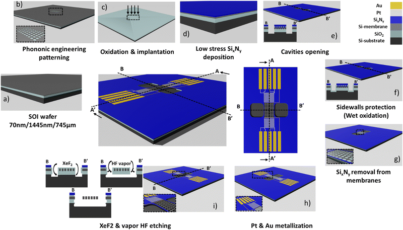 |
| | Fig. 3 Seebeck coefficient measurement device fabrication steps. | |
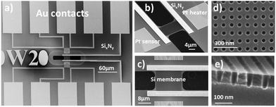 |
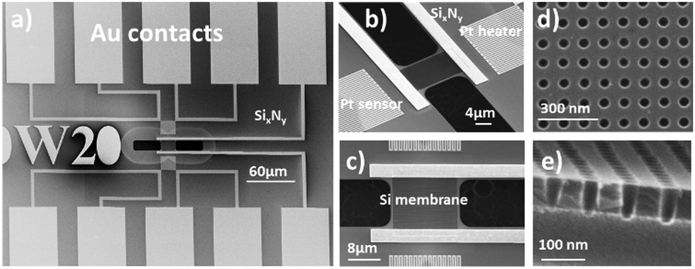
| | Fig. 4 (a) Seebeck coefficient measurement device illustrating the Au pads connected to the heater/sensor and the 20 μm × 20 μm Si membrane. (b) Close-up view of the suspended Si membrane and the Pt heater/sensor. (c) Top close-up view of the suspended PE Si membrane. (d) Details of the pore patterns on the Si membrane. (e) Cross-section view of the holes. | |
Metallic sensors and leads are formed through platinum and gold evaporation (h). Before metallization, a thermal oxide layer is grown on the Si membranes to protect the sidewalls from vapor phase xenon-difluoride (XeF2) etching (f). This final step in the device fabrication process involves suspending the silicon membranes using XeF2 and HF vapor etching to ensure their thermal insulation from the rest of the SOI substrate. The device features 10 pads for providing heating power, and measuring temperature difference and the Seebeck voltage. Samples were fabricated at lengths of 20 μm, 60 μm, 100 μm and 140 μm; each length is individually fabricated three times with widths of 10 μm, 20 μm and 30 μm. This leads to a total number of 12 geometries in both P and PE versions for each doping type (n-type and p-type) as detailed in the ESI.†
Seebeck coefficient
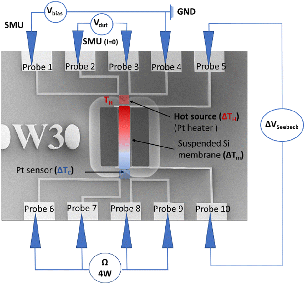
The devices were characterized using a thermometry technique, involving the determination of temperature difference based on the electrical resistance variation of the metal. The characterization process has two main steps. Firstly, the Pt heater serpentine is calibrated on a controlled heating chuck to extract the temperature coefficient of resistance (TCR), denoted as α. Secondly, the Pt heater is biased with a variable voltage. Based on the known α, the increase in electrical resistance due to the voltage variation is converted into temperature. In this case, the Pt film, which is 20 nm thin, exhibits a temperature coefficient of resistance α = 2.49 × 10⁻³ K−1 ± 2%. Fig. 5 illustrates the measurement protocol employed for determining the Seebeck coefficient.
 |
| | Fig. 5 Experimental setup for Seebeck coefficient measurement characterization. | |
The measurements are conducted using a face-to-face configuration with five probes. In this setup, the first probe is connected to the Keysight/Agilent E5281B SMU module, which applies a bias to the Pt heater. The second and third probes are connected to the Keysight/Agilent E5281A ATTO level high-resolution SMU module, enabling the measurement of the voltage across the Pt heater using a zero current source as a high impedance voltmeter. The fourth probe is connected to the ground. For the Pt sensor, the four probes (probe 6, 7, 8, and 9) are connected to an Agilent 34461A four-wire ohmmeter, allowing the measurement of the sensor's resistance. Additionally, an ammeter (Agilent 34401 A) is connected in series with the Agilent 34461A four-wire ohmmeter to control the injected current. By adjusting the calibration measurement range, very low current (1–2 μA) can be injected to avoid the self-heating via the Joule effect in the Pt sensor. Finally, the remaining two probes (probes 5 and 10), which are linked to the membrane, are connected to a Keysight/Agilent 34461A voltmeter. In the following, ΔTH = TH − T0 denotes the temperature difference between the hot side TH compared to the reference temperature T0 of the silicon substrate. Similarly, we obtain ΔTC = TC − T0. This setup allows the sensing of the voltage (ΔVSeebeck) generated by the temperature difference across the membrane (ΔTm= ΔTH − ΔTC). The Pt heater electrical resistance at various temperatures was determined using IC-CAP software which calculates the derivative of the voltage with respect to current, while the electrical resistance of the Pt sensor and the Seebeck voltage (ΔVSeebeck) were directly measured using the connected instruments.
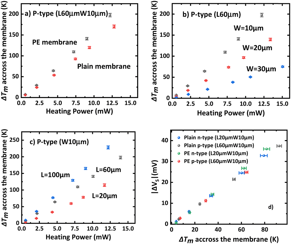
Fig. 6(a) presents the temperature difference along the membrane ΔTm. Notably, PE membranes demonstrate a higher temperature difference for a given heating power, indicating enhanced thermal gradient management or decreased thermal conductance across the membrane, as expected. Additionally, the temperature difference exhibits an increase with membrane length and a decrease with membrane width (Fig. 6b and c). The rise in thermal gradient with length can be attributed to the extended heat conduction pathway within the membrane. With an increased membrane length, heat traverses a longer distance, resulting in a larger temperature difference across the membrane. Conversely, the reduction in thermal gradient with width can be explained by the augmented cross-sectional area available for heat conduction. In Fig. 6d, the Seebeck voltage is plotted against the membrane's temperature difference (ΔTm). At ΔTm < 40 K, both PE and P membranes exhibit similar slopes. However, at higher ΔTm, a noticeable divergence occurs, emphasizing the dependence of the Seebeck coefficient with material properties and temperature rather than reflecting the geometric arrangement.
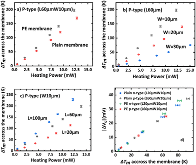 |
| | Fig. 6 Temperature difference across p-type silicon as a function of heating power for (a) P and PE membranes with dimensions 60 μm in length and 10 μm in width, (b) PE membranes with a fixed length of 60 μm and varying widths, and (c) PE membranes with a fixed width of 10 μm and varying lengths. (d) Absolute measured Seebeck voltage as a function of the temperature difference across different Si membranes. | |
Transient thermo-reflectance (TTR) was employed to validate the results obtained through the electrical measurements.
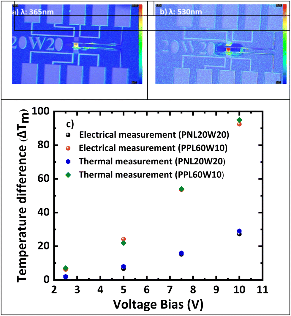
Fig. 7 illustrates thermal transient reflectance (TTR) images of an n-type Si plain membrane with dimensions (L = 20 μm, W = 20 μm) subjected to a voltage bias of 7.5 V. The figure presents two scenarios: (a) employing a 530 nm wavelength with a Pt coefficient of thermal reflectance of 1.2 × 10⁻⁴ K−1 for the determination of ΔTH and ΔTC, and (b) utilizing a 365 nm wavelength with a Si CTR of 1.37 × 10⁻⁴ K−1 for the determination of ΔTm. The temperature difference (ΔTm) observed across the suspended plain Si membrane through both electrical and thermal measurements are nearly identical (Fig. 7d), validating the accuracy of the previously determined Seebeck coefficient.
 |
| | Fig. 7 Thermal transient reflectance (TTR) images of n-type Si plain membranes (L = 20 μm, W = 20 μm) under a 7.5 V voltage bias, with (a) employing a 365 nm wavelength and Pt coefficient of thermal reflectance (CTR) of 1.2 × 10⁻⁴ K−1, and (b) using a 365 nm wavelength with Si CTR of 1.37 × 10⁻⁴ K−1. (c) Temperature difference as a function of voltage bias for plain; n-type (PNL20W20) and p-type (PPL60W10) membranes: comparison of electrical and thermal measurement techniques. | |
Thermal conductivity
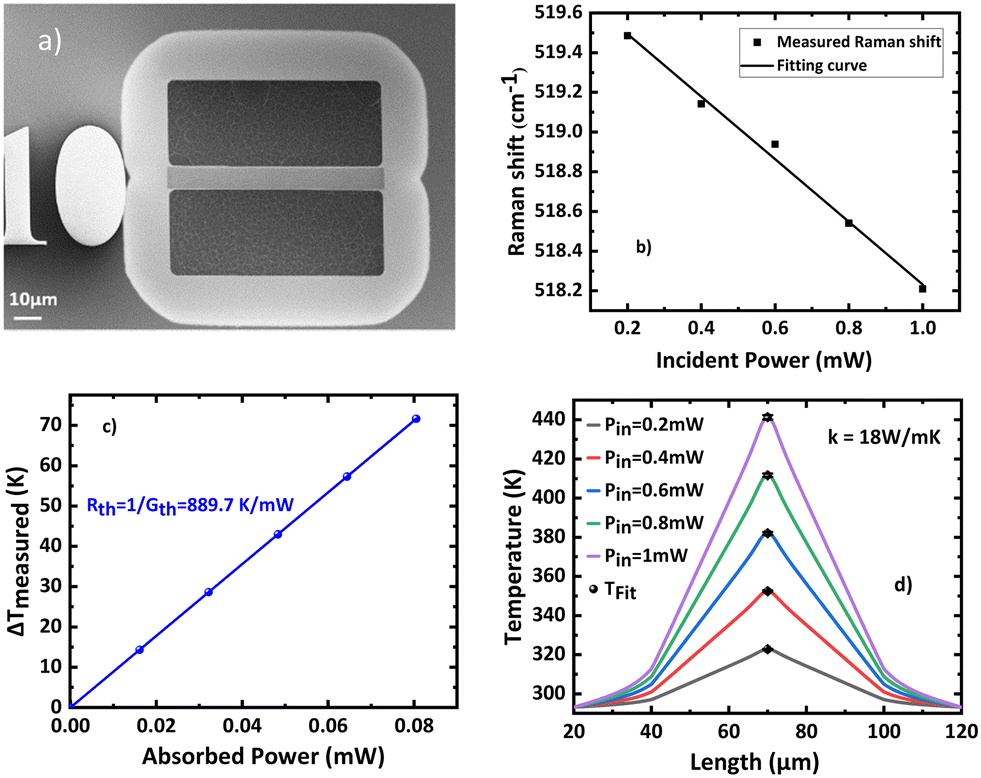
To quantify thermal conductivity, we used the single-laser Raman thermometry technique. This technique uses the temperature-dependent peak position in silicon42 to measure the local hot spot temperature rise ΔT originating from the excitation laser absorption. By using variable density, the intensity of the excitation laser can be varied, thus allowing the absorbed power Pabs to be tuned. It is then possible to measure the sample thermal conductance Gth = Pabs/ΔT. Finally, the thermal conductivity of the layer of interest must be de-embedded from the thermal conductance through modeling. It is thus useful to have the simplest sample geometry, and to make sure that the heat flow will be forced through the material of interest. For these reasons, additional membranes without electrodes are designed on the same substrate (Fig. 8a) and the sample is placed in a thermally regulated vacuum stage (Linkam HFS350-PB4) equipped with an optical window. We refer the reader to reported implementations of Raman thermometry43–45 and give more details about the setup used in the ESI† section.
 |
| | Fig. 8 (a) SEM image of a suspended membrane dedicated to Raman measurements. (b) Variation of Raman shift as a function of the incident power of a p-type plain membrane, t = 60 nm, L = 20 μm, W = 10 μm. (c) The experimental temperature difference across the p-type membrane with t = 60 nm, L = 60 μm and W = 10 μm as a function of the absorbed power (A = 8.05%). (d) p-type Si phononic membrane for parameterized power of the laser light incident into the middle of the membrane, κ =18 W m−1 K−1, absorption A = 10.9%, hole's diameter 45.8 nm and pitch = 100 nm. Black points are μTR experimental values. Membrane has the thickness t = 60 nm, L = 60 μm and W = 10 μm. Wing size of the device geometry equals 20 μm. | |
In our case, the laser is focused at the center of the membrane with a 50×/NA0.42 long-distance objective. The waist of the focused spot was measured to be 1.48 μm using the knife-edge method. Fig. 8b shows the silicon Raman diffusion peak position as a function of the absorbed power. The latter is obtained as Pin × A, where Pin is the measured incident power and A is the absorbance of the membranes calculated using the rigorous coupled wave analysis code RETICOLO.46 Making use of the reported coefficient ∂ω/∂T = −0.02 cm−1 K−1![[thin space (1/6-em)]](https://www.rsc.org/images/entities/char_2009.gif) 42 the shift of the Raman diffusion peak is converted into a temperature rise on Fig. 8c and Gth is obtained. Eventually, in order to extract the thermal conductivity κ, the membrane and its surrounding frame is modelled using the finite element software COMSOL. SixNy, buried oxide and silicon wafer thermal conductivities are assumed to be 1.55, 1.5 and 148 W m−1 K−1 respectively. The Gaussian laser source is modelled, and the stationary heat equation heat equation solved with κ as a parameter. Fig. 8d shows the temperature profiles obtained for each incident power value. The results show excellent agreement of the central temperature with the measurement by making use of a single thermal conductivity value. The agreement can be obtained within a ±1 W m−1 K−1 range.
42 the shift of the Raman diffusion peak is converted into a temperature rise on Fig. 8c and Gth is obtained. Eventually, in order to extract the thermal conductivity κ, the membrane and its surrounding frame is modelled using the finite element software COMSOL. SixNy, buried oxide and silicon wafer thermal conductivities are assumed to be 1.55, 1.5 and 148 W m−1 K−1 respectively. The Gaussian laser source is modelled, and the stationary heat equation heat equation solved with κ as a parameter. Fig. 8d shows the temperature profiles obtained for each incident power value. The results show excellent agreement of the central temperature with the measurement by making use of a single thermal conductivity value. The agreement can be obtained within a ±1 W m−1 K−1 range.
Results & discussion
Seebeck coefficient
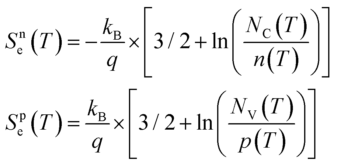
The Seebeck coefficients (S) for plain p-type, phonon engineered p-type, plain n-type, and phonon engineered n-type membranes were found to be 424 μV K−1, 440 μV K−1, −451 μV K−1, and −504 μV K−1, respectively. In a degenerate semiconductor, the total Seebeck coefficient (Stot) is influenced by two specific components: the diffusive contribution (Se) and the phonon drag contribution (Sph). The diffusive contribution originates from the migration of charge carriers in response to temperature gradients, while the phonon drag contribution arises from the exchange of momentum between the non-equilibrium phonon populations and the charge carriers. Previous studies by Geballe47 and Sadhu48 highlighted the significance of Sph in bulk Si at room temperature. Examining the impact of the phonon drag effect on the Seebeck coefficient in ultrathin SOI layers, F. Salleh et al.49 demonstrated its noteworthy influence near room temperature, particularly in the lightly doped region (ND < 1019 cm−3, where ND is the doping level). Furthermore, H. Ikeda et al.50 emphasized that the impurity band density of state (DOS) distribution primarily governs the Seebeck coefficient in heavily doped regions. The doping levels for plain p-type and n-type 60 nm membranes were measured to be 1.2 × 1019 cm−3 and 7.2 × 1018 cm−3, respectively. Correspondingly, their electrical conductivity values were measured at 100.8 S cm and 131.8 S cm, respectively. The diffusive contribution (Se) for plain p-type and n-type membranes is calculated using eqn (3) and amounts to 182 μV K−1 and −263 μV K−1 respectively.| |  | (3) |
where kB is the Boltzmann constant (1.38 × 10⁻²³ J K−1), q the elementary charge (1.602 × 10⁻¹⁹ C), h the Planck constant (6.62 × 10⁻³⁴ m2 kg s−1), p(T) and n(T) are the hole and electron volume densities respectively. NV(T) and NC(T) denote the effective density of states in valence and conduction bands, respectively.
The phonon drag contribution (Sph) is determined as 242 μV K−1 and −188 μV K−1 for plain p-type and n-type membranes, respectively. The calculation is based on the subtraction of the diffusive contribution (Se) from the total Seebeck coefficient (Stot). Sph represent 41% of the Stot of n-type membrane. Thus, we can confirm that the phonon-drag contribution at room temperature in 60 nm thin crystalline silicon is non-negligible. It is however commonly admitted that this effect should disappear in nanometric systems owing to the suppression of long mean-free path phonons. A temperature-dependent study of the phonon-drag Seebeck component, though beyond the scope of this study, will hopefully shed light on this finding.
Thermal conductivity
Incorporating patterns into the membrane design results in a notable decrease in thermal conductivity, with a reduction of about 56% observed for membranes with lengths of 20 μm and 100 μm, and a reduction of 42% for membranes with a length of 60 μm. This decrease can be attributed to several factors. Firstly, the introduction of patterns creates additional interfaces and boundaries within the membrane. These interfaces act as scattering sites for heat-carrying phonons, impeding their efficient propagation and resulting in a decrease in overall thermal conductivity. This can be also understood as a modification of the phonon mean free paths distribution towards lower values.51Fig. 9 illustrates the relationship between the thermal conductivity ratio of the phononic membrane (κh) to the thermal conductivity of the plain membrane (κP) and the porosity of the membrane. Our results fall within the typical range of thermal conductivity reduction already reported.
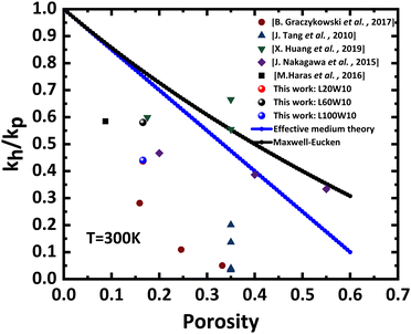 |
| | Fig. 9 The ratio of the phononic membrane to the thermal conductivity of the plain membrane as a function of the porosity. The graph includes experimental data from previous studies, as well as data from this current work, along with results obtained from effective medium theory and Maxwell–Eucken models. | |
Power factor and zT
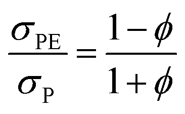
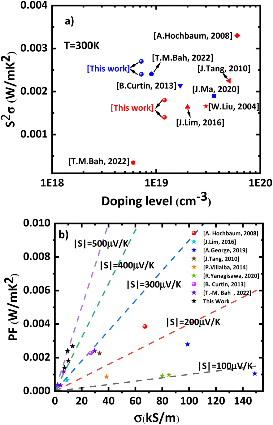
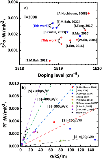
Fig. 10 presents the power factor (PF) of the studied membranes, illustrating the relationship between the power factor (S2σ) and the doping level for both n-type (blue) and p-type (red) silicon at a temperature of 300 K. The PF for plain membranes was determined using measured σP and SP, while for PE membranes, it was calculated using the effective medium theory (EMT) as described by eqn (4), involving parameters ϕ and σPE representing porosity and electrical conductivity of patterned membranes, respectively.| |  | (4) |
The near-identical S values for both P and PE suggest that the reduction in electrical conductivity in PE membranes is solely attributed to the patterned structure rather than other factors. The highest power factor achieved was 2.7 × 10⁻³ W m−1 K−2, corresponding to a specific doping level of 7.2 × 1018 cm−3 (n-type). In addition to our data, the graph also displays information on p-type nanostructured silicon. Specifically, it includes results from studies involving nanowires,26,52 holey silicon,32,53–55 and ultrathin solid films. The presence of phonon drags near room temperature in membranes has provided an opportunity to enhance the Seebeck coefficient. As a result, the power factor of these membranes has increased, reaching a level comparable to that of bulk Si at similar temperatures. According to the Ioffe plot presented in Fig. 10b, TE materials exhibiting the highest PF must be positioned the right and top ends.
 |
| | Fig. 10 Power factor as a function of (a) doping level. The graph includes experimental data from previous studies, as well as data from this current work, encompassing both n-type silicon (indicated in blue) and p-type silicon (represented in red) at a temperature of 300 K. (b) Electrical conductivity and Seebeck coefficient (Ioffe plot). | |
The reduced thermal conductivity observed in the membranes compared to bulk Si has contributed to a further increase in the zT (Fig. 1). To achieve a higher zT, it is recommended to focus on utilizing the phonon drag effect to further enhance the Seebeck coefficient while concurrently reducing the thermal conductivity. By capitalizing on these two aspects, it is possible to achieve an even larger figure of merit, thereby improving the overall thermoelectric performance of the membranes. Eventually the figure-of-merit obtained from measurements on single wafer devices range from 0.017 to 0.04. Table 1 summarizes the results measured and calculated.
Table 1 Summary of experimental values at room temperature for different silicon membrane types, including Seebeck coefficient, electrical conductivity, thermal conductivity, and zT figure of merit
| Type |
κ (W m−1 K−1) |
S
tot (μV K−1) |
S
e (μV K−1) |
S
ph (μV K−1) |
σ (kS m−1) |
zT
|
| p-Type plain |
31 |
424 |
182 |
242 |
10.08 |
0.017 |
| n-Type plain |
31 |
−451 |
−263 |
−188 |
13.18 |
0.026 |
| p-Type PE |
18 |
440 |
N/A |
N/A |
7.22 |
0.023 |
| n-Type PE |
18 |
−504 |
N/A |
N/A |
9.45 |
0.04 |
Conclusions
Values of the thermoelectric figure-of-merit in crystalline silicon nanostructures are scarce and disperse in literature reports. The methodology of such measurement is indeed challenging. Here, we report on devices fabricated on a single silicon-on-insulator substrate dedicated to the characterization of the Seebeck coefficient, electrical conductivity and thermal conductivity of 60 nm thick silicon membranes. The Seebeck coefficients for plain p-type, phonon engineered p-type, plain n-type, and phonon engineered n-type membranes were found to be 424 μV K−1, 440 μV K−1, −451 μV K−1, and −504 μV K−1, respectively. The highest power factor achieved was 2.7 × 10⁻³ W m−1 K−2, corresponding to a specific doping level of 7.2 × 1018 cm−3 for n-type membranes. The thermal conductivity was measured to be 31 W m−1 K−1 for a 60 nm thick Si membrane and 18 W m−1 K−1 for a porous Si membrane. We used resistive thermometry, transient thermo-reflectance and Raman thermometry to strengthen the quantitative evaluation of the Seebeck coefficient and thermal conductivity. Our findings support the possibility to increase the thermoelectric efficiency of crystalline silicon in nanonostructures. A further increase is obtained through porous patterning of the membranes. The figure-of-merit obtained from measurements on single wafer devices ranged from 0.017 to 0.04. However, we confirm that these values lie within the lower range of reported zT. Since our devices were designed with care of compatibility with conventional MEMS and CMOS processes, we suggest there is little chance that the high previously reported values can be reached in technologically plausible harvesters. Finally, we confirmed that the phonon-drag component of the Seebeck coefficient represents a non-negligible contribution even at room temperature in nanoscale systems.
Author contributions
H. I. is the main investigator. She designed, fabricated the samples, performed Seebeck and electrical conductivity measurements, visualized and interpreted the data and conducted the modelling for thermal conductivity quantification, and wrote the manuscript. A. P. performed the Raman thermometry measurements and contributed to their interpretation. J. C. contributed to the fabrication process development. E. O. set up the electrical characterization bench and contributed to the transient thermoreflectance measurement. E. B. modelled the optical absorbance of the porous membranes. E. D. contributed to the fabrication process, sample design and the manuscript. J.-F. R. supervised the project, established the methodology and contributed to the manuscript.
Conflicts of interest
The authors declare no potential scientific of financial conflicts of interest.
Acknowledgements
The authors are thankful to Alex Pip and the WELCOME‡ characterization centre for access to the transient thermoreflectance setup. H. I. was financially supported by Université de Lille. This work was supported by the French RENATECH network, the ST-IEMN Joint Research Lab, the European Research Council under the European Community's Seventh Framework Programme (FP7/2007–2013) ERC Grant Agreement no. 338179 and the French government through the National Research Agency (ANR) under project HANIBAL ANR-20-CE42-0019. This research work has been partially undertaken with the support of IEMN fabrication (CMNF) and characterization (PCMP) facilities.
Notes and references
- T. M. Bah, S. Didenko, D. Zhou, T. Zhu, H. Ikzibane, S. Monfray, T. Skotnicki, E. Dubois and J.-F. Robillard, Nanotechnology, 2022, 33, 505403 CrossRef CAS PubMed.
- Z. Wang, Y. van Andel, M. Jambunathan, V. Leonov, R. Elfrink and R. J. M. Vullers, J. Electron. Mater., 2011, 40, 499–503 CrossRef CAS.
- J. Xie, C. Lee and H. Feng, J. Microelectromech. Syst., 2010, 19, 317–324 CAS.
- A. P. Perez-Marín, A. F. Lopeandía, L. Abad, P. Ferrando-Villaba, G. Garcia, A. M. Lopez, F. X. Muñoz-Pascual and J. Rodríguez-Viejo, Nano Energy, 2014, 4, 73–80 CrossRef.
- D. Dávila, A. Tarancón, C. Calaza, M. Salleras, M. Fernández-Regúlez, A. San Paulo and L. Fonseca, Nano Energy, 2012, 1, 812–819 CrossRef.
- R. Yanagisawa, N. Tsujii, T. Mori, P. Ruther, O. Paul and M. Nomura, Appl. Phys. Express, 2020, 13, 095001 CrossRef CAS.
- R. Yanagisawa, P. Ruther, O. Paul, N. Tsujii, T. Mori and M. Nomura, IEEE, 2022, 114–116 Search PubMed.
- K. Ziouche, Z. Yuan, P. Lejeune, T. Lasri, D. Leclercq and Z. Bougrioua, J. Microelectromech. Syst., 2017, 26, 45–47 CAS.
- M. Haras and T. Skotnicki, Nano Energy, 2018, 54, 461–476 CrossRef CAS.
- M. Haras, V. Lacatena, F. Morini, J.-F. Robillard, S. Monfray, T. Skotnicki and E. Dubois, Mater. Lett., 2015, 157, 193–196 CrossRef CAS.
- D. Pinisetty and R. Devireddy, Acta Mater., 2010, 58, 570–576 CrossRef CAS.
- M. Očko, S. Žonja and M. Ivanda, MIPRO, 2010, 16–21 Search PubMed.
- Q. Hao, G. Zhu, G. Joshi, X. Wang, A. Minnich, Z. Ren and G. Chen, Appl. Phys. Lett., 2010, 97, 063109 CrossRef.
- J. S. Jin, J. Mech. Sci. Technol., 2014, 28, 2287–2292 CrossRef.
- M. Haras, V. Lacatena, F. Morini, J.-F. Robillard, S. Monfray, T. Skotnicki and E. Dubois, IEEE, 2014, 8.5.1–8.5.4 Search PubMed.
- P. Ferrando-Villalba, A. Lopeandia, L. Abad Muñoz, J. Llobet Sixto, M. Molina-Ruiz, G. Garcia, M. Gerbolès, F. X. Alvarez, A. Goñi, F. X. Munoz-Pascual and J. Rodríguez-Viejo, Nanotechnology, 2014, 25, 185402 CrossRef CAS PubMed.
- P. Ferrando-Villalba, A. P. Pérez-Marín, L. Abad, G. G. Dalkiranis, A. F. Lopeandia, G. Garcia and J. Rodriguez-Viejo, Nanomaterials, 2019, 9, 653 CrossRef CAS PubMed.
- Y. S. Ju, Appl. Phys. Lett., 2005, 87, 153106 CrossRef.
- M. Asheghi, Y. K. Leung, S. S. Wong and K. E. Goodson, Appl. Phys. Lett., 1997, 71, 1798–1800 CrossRef CAS.
- W. Liu and M. Asheghi, Appl. Phys. Lett., 2004, 84, 3819–3821 CrossRef CAS.
- E. Chávez-Ángel, J. S. Reparaz, J. Gomis-Bresco, M. R. Wagner, J. Cuffe, B. Graczykowski, A. Shchepetov, H. Jiang, M. Prunnila, J. Ahopelto, F. Alzina and C. M. Sotomayor Torres, APL Mater., 2014, 2, 012113 CrossRef.
- X. Huang, S. Gluchko, R. Anufriev, S. Volz and M. Nomura, ACS Appl. Mater. Interfaces, 2019, 11, 34394–34398 CrossRef CAS PubMed.
- J. Maire and M. Nomura, J. Appl. Phys., 2014, 53, 06JE09 CrossRef CAS.
- A. Boukai, Y. Bunimovich, J. Tahir-Kheli, J.-K. Yu, W. Goddard and J. Heath, Nature, 2008, 451, 168–171 CrossRef CAS PubMed.
- D. Li, Y. Wu, P. Kim, L. Shi, P. Yang and A. Majumdar, Appl. Phys. Lett., 2003, 83, 2934 CrossRef CAS.
- A. Hochbaum, R. Chen, R. Diaz, W. Liang, M. Najarian, A. Majumdar and P. Yang, Nature, 2008, 451, 163–167 CrossRef CAS PubMed.
- X. Huang, S. Gluchko, R. Anufriev, S. Volz and M. Nomura, ACS Appl. Mater. Interfaces, 2019, 11, 34394–34398 CrossRef CAS PubMed.
- M. Verdier, D. Lacroix, S. Didenko, J.-F. Robillard, E. Lampin, T.-M. Bah and K. Termentzidis, Phys. Rev. B, 2018, 97, 115435 CrossRef CAS.
- A. George, R. Yanagisawa, R. Anufriev, J. He, N. Yoshie, N. Tsujii, Q. Guo, T. Mori, S. Volz and M. Nomura, ACS Appl. Mater. Interfaces, 2019, 11, 12027–12031 CrossRef CAS PubMed.
- J. Nakagawa, Y. Kage, T. Hori, J. Shiomi and M. Nomura, Appl. Phys. Lett., 2015, 107, 023104 CrossRef.
- M. Haras, V. Lacatena, T. M. Bah, S. Didenko, J.-F. Robillard, S. Monfray, T. Skotnicki and E. Dubois, IEEE Electron Device Lett., 2016, 37, 1358–1361 CAS.
- J. Tang, H.-T. Wang, D. H. Lee, M. Fardy, Z. Huo, T. Russell and P. Yang, Nano Lett., 2010, 10, 4279–4283 CrossRef CAS PubMed.
- R. Yanagisawa and M. Nomura, J. Phys.: Conf. Ser., 2019, 1407, 012013 CrossRef CAS.
- M. Nomura, J. Nakagawa, K. Sawano, J. Maire and S. Volz, Appl. Phys. Lett., 2016, 109, 173104 CrossRef.
- B. Graczykowski, A. El Sachat, J. S. Reparaz, M. Sledzinska, M. R. Wagner, E. Chavez-Angel, Y. Wu, S. Volz, Y. Wu, F. Alzina and C. M. Sotomayor Torres, Nat. Commun., 2017, 8, 415 CrossRef CAS PubMed.
- Q. Hao, D. Xu, H. Zhao, Y. Xiao and F. J. Medina, Sci. Rep., 2018, 8, 9056 CrossRef PubMed.
- M. R. Wagner, B. Graczykowski, J. S. Reparaz, A. El Sachat, M. Sledzinska, F. Alzina and C. M. Sotomayor Torres, Nano Lett., 2016, 16, 5661–5668 CrossRef CAS PubMed.
- D. Li, Y. Wu, P. Kim, L. Shi, P. Yang and A. Majumdar, Appl. Phys. Lett., 2003, 83, 2934–2936 CrossRef CAS.
- V. Lacatena, M. Haras, J.-F. Robillard, S. Monfray, T. Skotnicki and E. Dubois, Microelectron. Eng., 2014, 121, 131 CrossRef CAS.
- E. Dechaumphai and R. Chen, J. Appl. Phys., 2012, 111, 073508 CrossRef.
- R. Yanagisawa, J. Maire, A. Ramiere, R. Anufriev and M. Nomura, Appl. Phys. Lett., 2017, 110, 133108 CrossRef.
- M. Balkanski, R. F. Wallis and E. Haro, Phys. Rev. B: Condens. Matter Mater. Phys., 1983, 2(8), 1928–1934 CrossRef.
- P. J. Newby, B. Canut, J.-M. Bluet, S. Gomès, M. Isaiev, R. Burbelo, K. Termentzidis, P. Chantrenne, L. G. Fréchette and V. Lysenko, J. Appl. Phys., 2013, 114, 014903 CrossRef.
- E. Chávez-Ángel, J. S. Reparaz, J. Gomis-Bresco, M. R. Wagner, J. Cuffe, B. Graczykowski, A. Shchepetov, H. Jiang, M. Prunnila, J. Ahopelto, F. Alzina and C. M. Sotomayor Torres, APL Mater., 2014, 2, 012113 CrossRef.
- B. Stoib, S. Filser, J. Stötzel, A. Greppmair, N. Petermann, H. Wiggers, G. Schierning, M. Stutzmann and M. S. Brandt, Semicond. Sci. Technol., 2014, 29, 124005 CrossRef.
-
J. P. Hugonin and P. Lalanne, RETICOLO software for grating analysis, Institut d'Optique, Orsay, France, 2005, arXiv:2101:00901 DOI:10.48550/arXiv.2101.00901.
- T. H. Geballe and G. W. Hull, Phys. Rev., 1955, 98, 940–947 CrossRef CAS.
- J. Sadhu,
et al.
, Nano Lett., 2015, 15, 3159–3165 CrossRef CAS PubMed.
- F. Salleh, T. Oda, Y. Suzuki, Y. Kamakura and H. Ikeda, Appl. Phys. Lett., 2014, 105, 102104 CrossRef.
- H. Ikeda and F. Salleh, Appl. Phys. Lett., 2010, 96, 012106 CrossRef.
- A. M. Massoud, V. Lacatena, M. Haras, E. Dubois, S. Monfray, J.-M. Bluet, P.-O. Chapuis and J.-F. Robillard, APL Mater., 2022, 10, 051113 CrossRef CAS.
- B. M. Curtin, E. A. Codecido, S. Krämer and J. E. Bowers, Nano Lett., 2013, 13, 5503–5508 CrossRef CAS PubMed.
- J. Lim,
et al.
, ACS Nano, 2016, 10, 124–132 CrossRef CAS PubMed.
- J. Ma, D. Gelda, K. V. Valavala and S. Sinha, J. Appl. Phys., 2020, 128, 115109 CrossRef CAS.
- N. Liu, T. Zhu, M. G. Rosul, J. Peters, J. E. Bowers and M. Zebarjadi, Mater. Today Phys., 2020, 14, 100224 CrossRef.
|
| This journal is © The Royal Society of Chemistry 2024 |
Click here to see how this site uses Cookies. View our privacy policy here. 
 Open Access Article
 This Open Access Article is licensed under a Creative Commons Attribution-Non Commercial 3.0 Unported Licence
 a,
Akash
Patil
ab,
Jon
Canosa
a,
Etienne
Okada
a,
Etienne
Blandre
a,
Emmanuel
Dubois
a and
Jean-François
Robillard
*a
a,
Akash
Patil
ab,
Jon
Canosa
a,
Etienne
Okada
a,
Etienne
Blandre
a,
Emmanuel
Dubois
a and
Jean-François
Robillard
*a