
 Open Access Article
 This Open Access Article is licensed under a Creative Commons Attribution-Non Commercial 3.0 Unported Licence
Co-sputtered phase-change Ga–Sb–Te thin films†
Magdalena
Kotrla
a,
Petr
Janíček
bc,
Jan
Gutwirth
a,
Tomáš
Halenkovič
a,
Jan
Přikryl
c,
Stanislav
Šlang
 c,
François
Cheviré
d,
Virginie
Nazabal
da and
Petr
Němec
*a
c,
François
Cheviré
d,
Virginie
Nazabal
da and
Petr
Němec
*a
aDepartment of Graphic Arts and Photophysics, Faculty of Chemical Technology, University of Pardubice, Studentská 95, 53210 Pardubice, Czech Republic. E-mail: petr.nemec@upce.cz
bInstitute of Applied Physics and Mathematics, Faculty of Chemical Technology, University of Pardubice, Studentská 95, 532 10 Pardubice, Czech Republic
cCenter of Materials and Nanotechnologies, Faculty of Chemical Technology, University of Pardubice, Studentská 95, 532 10 Pardubice, Czech Republic
dUniv Rennes, CNRS, ISCR (Institut des Sciences Chimiques de Rennes) – UMR 6226, F-35000 Rennes, France
First published on 20th June 2024
Abstract
Thin films with compositions equally distributed through GaSb–GaTe and GaSb–Te tie-lines were fabricated by radio-frequency magnetron co-sputtering. Several characterization techniques (scanning electron microscopy with energy-dispersive X-ray analysis, temperature dependent grazing incidence X-ray diffraction, Raman scattering spectroscopy, variable angle spectroscopic ellipsometry and sheet resistance temperature dependences) were employed to evaluate the properties of both as-deposited and annealed Ga–Sb–Te films. The change in the crystallization temperature influenced by composition variations is studied along with the change in the optical properties upon crystallization induced by annealing. The optical contrast between the annealed and amorphous states at a wavelength of 405 nm reaches a value of ∼1.85 which is comparable with that in the case of commercially used Ge2Sb2Te5. All films showed a drop in temperature-dependent sheet resistance (∼4–7 orders of magnitude) except for Ga5Sb2Te3 and Ga5SbTe4. The results obtained from X-ray diffraction reveal Sb, GaSb, gallium antimony telluride together with Sb2Te3 and Te as possible phases which appear in the films after annealing. Additionally, Raman spectra revealed vibrational modes between Ga and Sb, vibrations of Sb–Sb bonds, vibrations of Te–Te and vibrations of Sb–Te.
Introduction
Ge–Sb–Te (GST), particularly the Ge2Sb2Te5 composition, stands out as the most investigated and commercially employed phase-change material system.1 The active layers of phase-change materials should fulfil the necessary qualities for promising data recording, such as glass formation (writability), a large signal/noise ratio (readability), fast recrystallization (erasibility), a stable amorphous phase (archival storage, operation at elevated temperatures), and stable composition (cyclability).2 To satisfy all the requirements is challenging as high speed crystallization is usually in contrast to high amorphous phase stability and a low media signal/noise ratio.3 Therefore, many attempts and several approaches were made to achieve the best combination of the above-mentioned properties of phase change materials. Some studies suggest theoretical predictions,4 some of them tried adding or doping different elements to Sb–Te such as mostly known Ag and In, or Al,5 and Sc,6 doping of GST with many elements such as N, C, Sc, and Cr,6–9 or varying GST stoichiometry.10,11One of the approaches suggested in the literature is doping of Ga into Sb–Te to increase the crystallization rate.3 Ga–Sb–Te, more specifically the eutectic Ga6Sb5Te, was already studied in the sixties by Kurata12 from the point of view of semiconductor thermoelectric and optical properties. Later, Lankhorst et al. discovered that the Sb–Te material doped with Ga presents a fast-crystallization rate and low media noise.3 Furthermore, the crystallization kinetics of some compositions in the Ga–Sb–Te ternary system was studied by means of nonisothermal differential scanning calorimetry by Lee et al.13,14 The outcome of the study led to a discussion on the topic of activation energy of phase transition, determination of kinetic exponents, and estimation of crystallization time. Samples Ga6.32Sb68.01Te25.67, Ga13.68Sb65.14Te21.18, Ga12.03Sb44.90Te43.07, and Ga20.68Sb48.28Te31.07 were evaluated as compositions with potential applications in phase-change materials. The crystallization speed ranged from 40 s to 50 s, and the crystallization temperature TC varied between approximately 130 and 270 °C (an increase in TC observed with the addition of Ga in the material). Cheng et al. focused on stoichiometric Ga4Sb6Te3 which shows a high TC of 271 °C (higher than GST having Tx in the range of 150–170 °C), fast crystallization speed, high crystallization temperature and high electrical contrast.15 Lu et al. studied switching between amorphous and crystalline phases of GaSb5Te4 for 6.7 × 10⁴ cycles.16 Other papers investigated Ga–Sb–Te materials in the context of thermoelectric properties17 and mainly electrical memories showing that Ga2Sb5Te3 cells require 25% less RESET current than GST cells with ultralong data retention18 and Ga25Sb67Te8 and Ga18Sb70Te12 have a TC above 245 °C and activation energy of crystallization greater than 5 eV.19 Si-doped GaSbTe quaternary materials have been evaluated to be temperature-robust with fast switching characteristics.20 Memory-cells made of Ga18Sb70Te12 can be set–reset at 20–500 ns with electrical currents around 66% of those of Ge2Sb2Te5 cells.21 Large variation in electrical contrast (up to 8 orders of magnitude) together with high optical contrast (4.2) was found for Ga26Sb20Te54 thin layers.22 Phase-change optical disks with GaSbTe recording media were prepared in the DVD + RW format.23 In general, it is worth mentioning that molecular dynamics calculations can be used to predict the mechanical and electronic properties of Te containing materials.24,25 In the case of Ga–Sb–Te, DFT studies using molecular dynamics simulation of the amorphous ternary system were reported by Bouzid et al. concluding that there are two binary tetrahedral-like compounds GaTe and GaSb and elemental Sb, but very few Sb–Te bonds.26
This study aims to fabricate novel films within the Ga–Sb–Te system by substituting Ga for Ge in GST, which should have a significant influence on both the phases likely to crystallize and the electronic structure of the material, while also investigating the effects of higher Te concentrations in the deposited layers. Moreover, there is a motivation to study the unexplored part of the Ga–Sb–Te ternary diagram that has not been investigated in prior literature.11,15,23,27 Thus, the layers with compositions equally distributed through GaSb–GaTe and GaSb–Te tie-lines were prepared in GaSb![[thin space (1/6-em)]](https://www.rsc.org/images/entities/char_2009.gif) :GaTe ratios, respectively GaSb:Te 80:20, 60:40, 40:60, 20:80, and 10:90. The characterization of the prepared thin films in both the as-deposited (amorphous) state and annealed (crystalline) state was performed via several techniques such as energy-dispersive X-ray analysis (EDX), X-ray diffraction (XRD), temperature dependent grazing incidence X-ray diffraction (TD-GI-XRD), Raman scattering spectroscopy, temperature dependent electrical resistivity, atomic force microscopy (AFM), and variable angle spectroscopic ellipsometry (VASE).
:GaTe ratios, respectively GaSb:Te 80:20, 60:40, 40:60, 20:80, and 10:90. The characterization of the prepared thin films in both the as-deposited (amorphous) state and annealed (crystalline) state was performed via several techniques such as energy-dispersive X-ray analysis (EDX), X-ray diffraction (XRD), temperature dependent grazing incidence X-ray diffraction (TD-GI-XRD), Raman scattering spectroscopy, temperature dependent electrical resistivity, atomic force microscopy (AFM), and variable angle spectroscopic ellipsometry (VASE).
Experimental
RF magnetron co-sputtering in Ar plasma was performed at room temperature employing a MPE600 multichamber deposition system (Plassys-Bestek, France). Three two-inch targets GaSb, GaTe (both 99.999% purity) and Te (99.99% purity) were used (ALB Materials, USA). The following substrates were utilized: soda-lime microscope slide glass (Knittel, Germany), borosilicate BK7 glass (Crystran, UK), and single-crystalline (100) silicon wafers (OnSemi, Czechia). The substrates were cleaned prior to the depositions using soap, distilled water, and isopropyl alcohol and afterwards by RF Ar plasma in the load lock. The deposition conditions were as follows: background pressure ≤1 × 10⁻⁵ Pa (typically ≤5 × 10⁻⁶ Pa), an average target-to-substrate distance of 9 cm, an Ar pressure of 0.5 Pa, an Ar flow rate of 75 sccm, and a substrate holder rotation of 5 rpm. The abovementioned experimental conditions were kept constant except for the applied powers on individual cathodes (maximally 35 W for GaSb, 15 W for GaTe and 10 W for the Te cathode) and changes in deposition time. Due to the experimental conditions used (position of the substrates on the substrate holder), we expect that the chemical compositions remain homogeneous within the deposited area. The increase of temperature of the substrate holder during the deposition of thin films was negligible (from room temperature (∼20 °C) by 1.5 °C at maximum). The deposition conditions resulting in the required chemical compositions were tailored by applying the methodology described in ref. 28.The chemical composition of the films was verified by two scanning electron microscopes combined with EDX analyzers: 300 LA EDS (Jeol, Japan) and Aztec X-Max 20 (Oxford Instruments, UK). Thin films of each composition were annealed at temperatures above Tc (450 °C for Ga5Sb4Te, Ga4Sb4Te, Ga3Sb3Te2 and Ga2Sb2Te3, 470 °C for Ga5Sb3Te2, 350 °C for GaSbTe4 and 340 °C for GaSbTe9) in an Ar atmosphere for analysis in the crystalline state. XRD data were collected for both as-deposited and annealed layers using two instruments. First one (MiniFlex 600, Rigaku, Japan) equipped with a 1D detector D/teX Ultra measured in the theta 2 theta position recorded diffractograms at room temperature with CuKα radiation from 20° ≤ 2θ ≤ 60° within 0.01 or 0.02° steps. The second diffractometer (X'pert Pro, Malvern PANalytical, UK) used in Bragg–Brentano geometry, equipped with a X’Celerator detector and an Anton Paar HTK 1200 oven chamber, measured data within the 20° ≤ 2θ ≤ 60° range with CuKα radiation. XRD patterns were collected under the flow of He with steps of 10 or 5 °C for different temperatures. The heating rate was set at 2° min−1 between each data collection step.
The optical properties were studied exploiting two variable angle spectroscopic ellipsometers (VASE and IR-VASE, both J. A. Woollam Co., Inc., USA) in the spectral range of 280 nm–10 μm. The first ellipsometer with an automatic rotating analyzer was used for the UV-Vis-NIR region, measuring 100 revolutions with a wavelength step of 20 nm at selected angles of incidence (50°, 60°, and 70°). The second ellipsometer with a rotating compensator was employed for the IR region at angles of incidence as above (50 scans, 15 spectra per revolution, resolution of 8 cm−1). For the analysis of the as-deposited thin films’ ellipsometric data, the Cody–Lorentz (CL) model, which includes the correct band edge function, a description of the weak Urbach absorption tail, as well as a Lorentz oscillator, was applied.29 For the annealed/crystalline samples, a parameterized semiconductor oscillator function together with Drude-type contribution for free carriers and another Lorentz oscillator for interband transitions for higher photon energies were utilized.
Temperature-dependent measurements of sheet resistance (Rs) were conducted using a custom-built setup and the four-point probe van der Pauw based method.30 The measurements were performed under an Ar flow with a heating rate of 2 °C min−1.
Raman scattering data of the films were recorded in backscattering geometry using a high-spectral-resolution LabRAM HR Evolution Raman Spectrometer (HORIBA Scientific, France) coupled to a confocal microscope with a 100× objective. Raman scattering spectra were recorded using a laser operating at 785 nm with power in the range of a few milliwatts to prevent the photoinduced changes and the grating had a groove density of 600 grooves per mm. The measured Raman spectra were reduced by the Shuker–Gammon relationship.31
Atomic force microscopy (AFM, Solver NEXT, NT-MDT, Ireland in a semi-contact mode) was used to examine the surface topography and roughness of all the films being studied.
Results and discussion
An overview of Ga–Sb–Te thin layers’ chemical composition investigated previously by different authors together with the thin films’ compositions studied in this work is given in Fig. 1. Nominal chemical compositions of the thin films to be fabricated in this study are as follows: Ga5Sb4Te, Ga5Sb3Te2, Ga5Sb2Te3, Ga5SbTe4, Ga4Sb4Te, Ga3Sb3Te2, Ga2Sb2Te3, GaSbTe4 and GaSbTe9. To obtain co-sputtered Ga–Sb–Te thin films with two different thicknesses (∼100 and ∼170 nm) for use in different characterization techniques, two sets of depositions were performed. The compositions of thin films determined by EDX are summarized in Table 1 and Fig. 1 for the as-deposited films (∼100 nm thick) as well as for the annealed films (∼170 nm) with the exception of Ga5Sb2Te3 and Ga5SbTe4 where the layers evaporated during annealing. As depicted in Table 1 and Fig. 1, the measured compositions of both as-deposited and annealed samples are in good agreement with the nominal ones.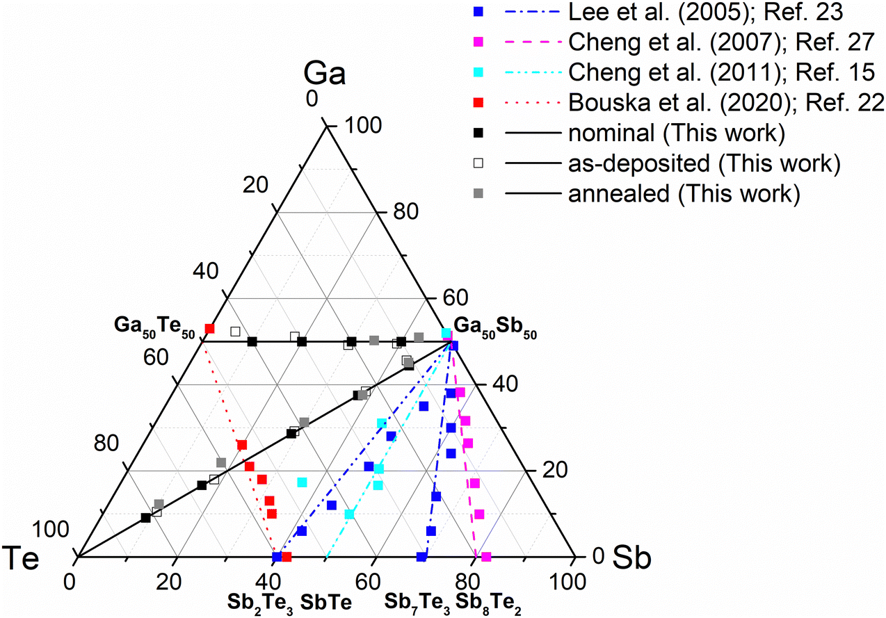 | ||
| Fig. 1 Ternary Ga–Sb–Te diagram showing the chemical composition of thin films previously studied in the literature15,22,23,27 and films fabricated in this work (GaSb–GaTe and GaSb–Te tie-lines). Comparison of the chemical composition of the nominal, as-deposited, and annealed co-sputtered Ga–Sb–Te thin films is shown as well. | ||
| Nominal composition in percentage representation (%) | Nominal composition (at%) | Measured composition of as-deposited films (at%) | Measured composition of annealed films (at%) | ||
|---|---|---|---|---|---|
| GaSb | GaTe | Te | |||
| 80 | 20 | — | Ga50Sb40Te10 (Ga5Sb4Te) | Ga50Sb39Te11 | Ga50Sb39Te11 |
| 60 | 40 | — | Ga50Sb30Te20 (Ga5Sb3Te2) | Ga49Sb30Te21 | Ga49Sb30Te21 |
| 40 | 60 | — | Ga50Sb20Te30 (Ga5Sb2Te3) | Ga51Sb18Te31 | NA |
| 20 | 80 | — | Ga50Sb10Te40 (Ga5SbTe4) | Ga52Sb6Te42 | NA |
| 80 | — | 20 | Ga45.6Sb43.3Te11.1 (Ga4Sb4Te) | Ga46Sb43Te11 | Ga45Sb44Te11 |
| 60 | — | 40 | Ga38.4Sb38.6Te22.9 (Ga3Sb3Te2) | Ga38Sb39Te23 | Ga38Sb38Te24 |
| 40 | — | 60 | Ga29.2Sb28.9Te41.9 (Ga2Sb2Te3) | Ga29Sb29Te42 | Ga31Sb30Te39 |
| 20 | — | 80 | Ga18Sb18.4Te63.6 (GaSbTe4) | Ga18Sb18Te64 | Ga22Sb18Te60 |
| 10 | — | 90 | Ga10.4Sb10.6Te79 (GaSbTe9) | Ga10Sb11Te79 | Ga12Sb10Te78 |
The crystallization temperatures Tc (Table 2) were evaluated based on thin films’ temperature dependent sheet resistance measurements (Fig. 2) as peaks of d(lnRs)/d(T) 1st derivatives. All layers deposited on soda-lime glass showed a drop in Rs (∼4–7 orders of magnitude) except for Ga5Sb2Te3 and Ga5SbTe4, which are the samples containing 60% and more of GaTe. Except for not showing a rapid phase change, the Ga5Sb2Te3 layer exhibits low stability and changes the state of matter (i.e. evaporated) around 320 °C. According to the Rs results supported by TD-GI-XRD data, the crystallization is not visible for the Ga5SbTe4 film. The thin films from the GaSb–GaTe tie-line tend to decrease their crystallization temperature from 340 to 315 °C with the higher content of GaTe. On the other hand, the crystallization temperatures of the layers from the GaSb–Te tie-line are lower and gradually decrease from ∼305 to ∼100 °C with increasing content of Te. It is worth noting that the temperatures of crystallization obtained from temperature dependent Rs measurements are in very good agreement with those determined by TD-GI-XRD exemplified by Fig. 3 (the remaining TD-GI-XRD data are presented in the ESI†).
| Composition | T c (°C) | Δn + i Δk (405 nm) | |Δn| + |Δk| (405 nm) | d annealed/das-deposited |
|---|---|---|---|---|
| Ga5Sb4Te | 338 | −1.38 − i 0.45 | 1.83 | 1.00 |
| Ga5Sb3Te2 | 313 | −0.96 + i 0.04 | 1.00 | 0.93 |
| Ga4Sb4Te | 304 | −0.63 − i 0.18 | 0.81 | 0.98 |
| Ga3Sb3Te2 | 295 | −0.67 − i 0.00 | 0.67 | 0.98 |
| Ga2Sb2Te3 | 214 | −1.01 − i 0.15 | 1.16 | 0.92 |
| GaSbTe4 | 128 | −1.15 + i 0.29 | 1.44 | 0.95 |
| GaSbTe9 | 100 | −1.65 + i 0.20 | 1.85 | 0.94 |
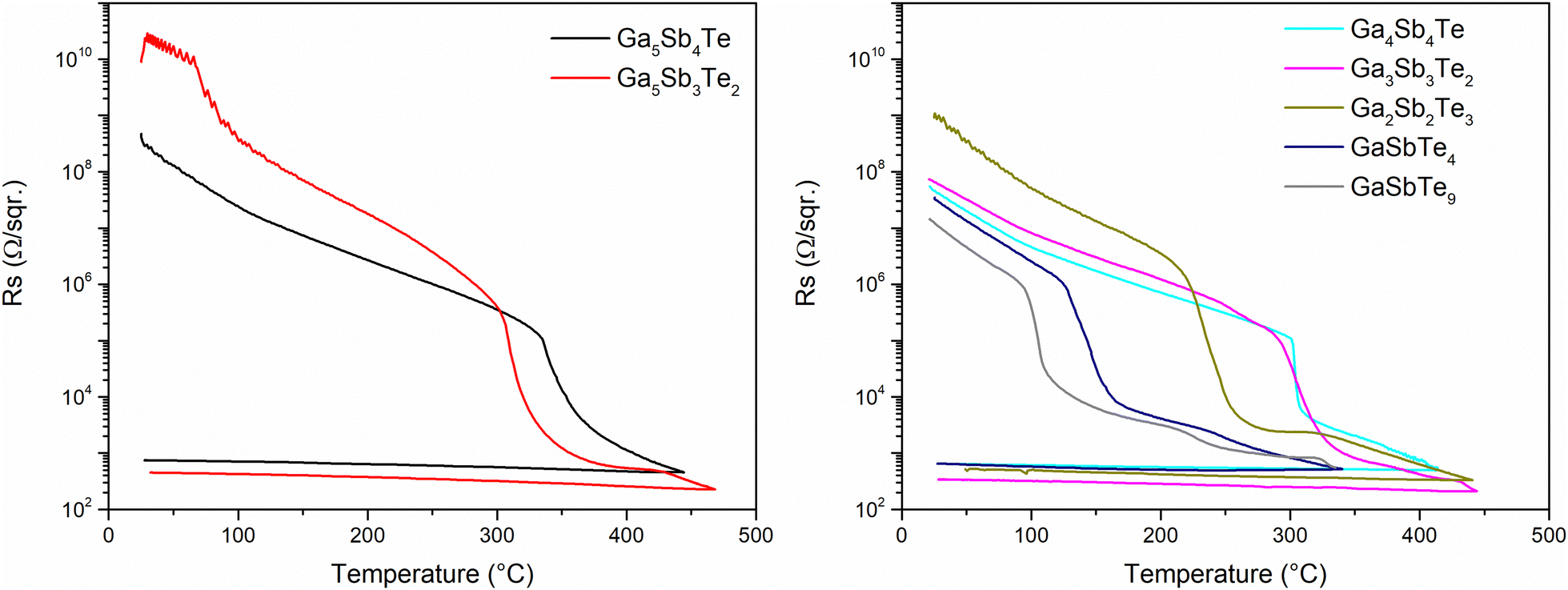 | ||
| Fig. 2 Temperature-dependent sheet resistance of Ga–Sb–Te thin films with a thickness of ∼100 nm deposited on the glass substrate (heating rate of 2 °C min−1). | ||
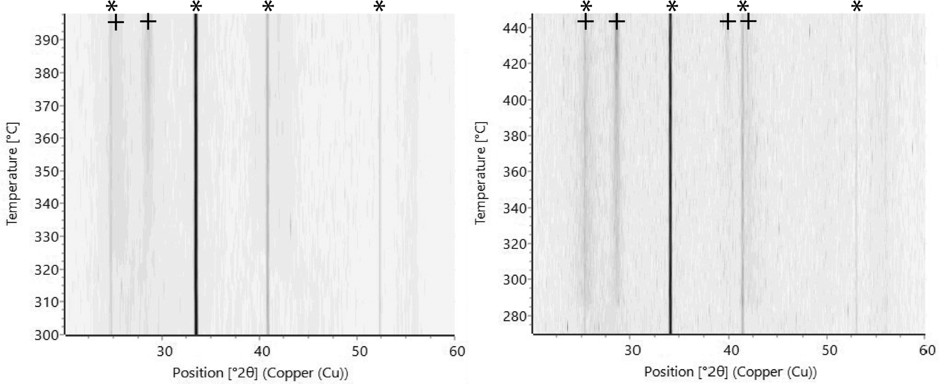 | ||
| Fig. 3 The examples of temperature-dependent XRD plots of Ga5Sb4Te (left) and Ga4Sb4Te (right) thin films (100 nm). The ‘*’ symbol denotes the peaks originating from the substrate, and the ‘+’ symbol denotes the peaks originating from the layer. | ||
Analyzing the TD-GI-XRD data of thinner (∼100 nm) co-sputtered Ga–Sb–Te thin films turned out to be challenging due to the limited number of peaks observed. Consequently, it was difficult to assign the crystalline phase(s) accurately from the available crystallographic ICCD PDF-2 (released 2016) database32 so the measured temperature-dependent diffractograms were supported by additional XRD measurements performed at room-temperature for thicker (∼170 nm) Ga–Sb–Te layers annealed for 2 hours at temperatures above TC (specified in Fig. 4) in the ambient Ar atmosphere with a heating rate of 2 °C min−1. The diffractograms presented in Fig. 4 revealed more peaks than in the case of GI-TD-XRD measurements. For the samples with less than 40% of Te (Ga5Sb4Te, Ga5Sb3Te2, Ga4Sb4Te, and Ga3Sb3Te2), the peaks around ∼25.5°, ∼28.8°, ∼40.2°, and ∼42.4° are observed in accordance with ref. 19, 20 and 27 for Ga–Sb–Te alloys. Cheng et al.27 measured the DTA of Sb-rich Ga–Sb–Te films claiming one visible exothermal peak (one temperature of crystallization) and therefore assuming one crystalline phase present in the alloy. The diffractions of the above-mentioned thin films’ compositions can be assigned to trigonal Sb (R![[3 with combining macron]](https://www.rsc.org/images/entities/char_0033_0304.gif) m, PDF card no. 01-085-1324) as shown in Fig. 4 at the very bottom. It is worth mentioning that cubic GaSb (F
m, PDF card no. 01-085-1324) as shown in Fig. 4 at the very bottom. It is worth mentioning that cubic GaSb (F![[4 with combining macron]](https://www.rsc.org/images/entities/char_0034_0304.gif) 3m, PDF card no. 03-065-8397) exhibits diffraction peaks at 2 theta equal to 25.3°, 29.3° and 41.9° and cubic GaSb0.89Te0.11 and cubic Ga0.838Sb0.515Te0.485 exhibit diffraction peaks at very close 2 theta positions of 25.4°, 29.4° and 42.0° (GaSb0.89Te0.11, F3m, PDF card no. 01-071-4517), and 25.7°, 29.8° and 42.6° (Ga0.838Sb0.515Te0.485, F3m, PDF card no. 01-089-3665), respectively; therefore the existence of GaSb and/or gallium antimony telluride in annealed layers cannot be excluded in our case. On the other hand, samples’ diffractograms with more than 40% of Te (Ga2Sb2Te3, Ga2Sb2Te3, and Ga2Sb2Te3) exhibit more diffraction peaks which can be related to trigonal Sb2Te3 (Rm, PDF card no. 01-083-5987) and hexagonal Te (P3121, PDF card no. 01-079-0736), as depicted in Fig. 4 together with trigonal Sb (Rm, PDF card no. 01-085-1324), cubic GaSb (F3m, PDF card no. 03-065-8397), trigonal Sb2Te3 (Rm, PDF card no. 01-083-5987) and hexagonal Te (P3121, PDF card no. 01-079-0736) lines from the database.32
3m, PDF card no. 03-065-8397) exhibits diffraction peaks at 2 theta equal to 25.3°, 29.3° and 41.9° and cubic GaSb0.89Te0.11 and cubic Ga0.838Sb0.515Te0.485 exhibit diffraction peaks at very close 2 theta positions of 25.4°, 29.4° and 42.0° (GaSb0.89Te0.11, F3m, PDF card no. 01-071-4517), and 25.7°, 29.8° and 42.6° (Ga0.838Sb0.515Te0.485, F3m, PDF card no. 01-089-3665), respectively; therefore the existence of GaSb and/or gallium antimony telluride in annealed layers cannot be excluded in our case. On the other hand, samples’ diffractograms with more than 40% of Te (Ga2Sb2Te3, Ga2Sb2Te3, and Ga2Sb2Te3) exhibit more diffraction peaks which can be related to trigonal Sb2Te3 (Rm, PDF card no. 01-083-5987) and hexagonal Te (P3121, PDF card no. 01-079-0736), as depicted in Fig. 4 together with trigonal Sb (Rm, PDF card no. 01-085-1324), cubic GaSb (F3m, PDF card no. 03-065-8397), trigonal Sb2Te3 (Rm, PDF card no. 01-083-5987) and hexagonal Te (P3121, PDF card no. 01-079-0736) lines from the database.32
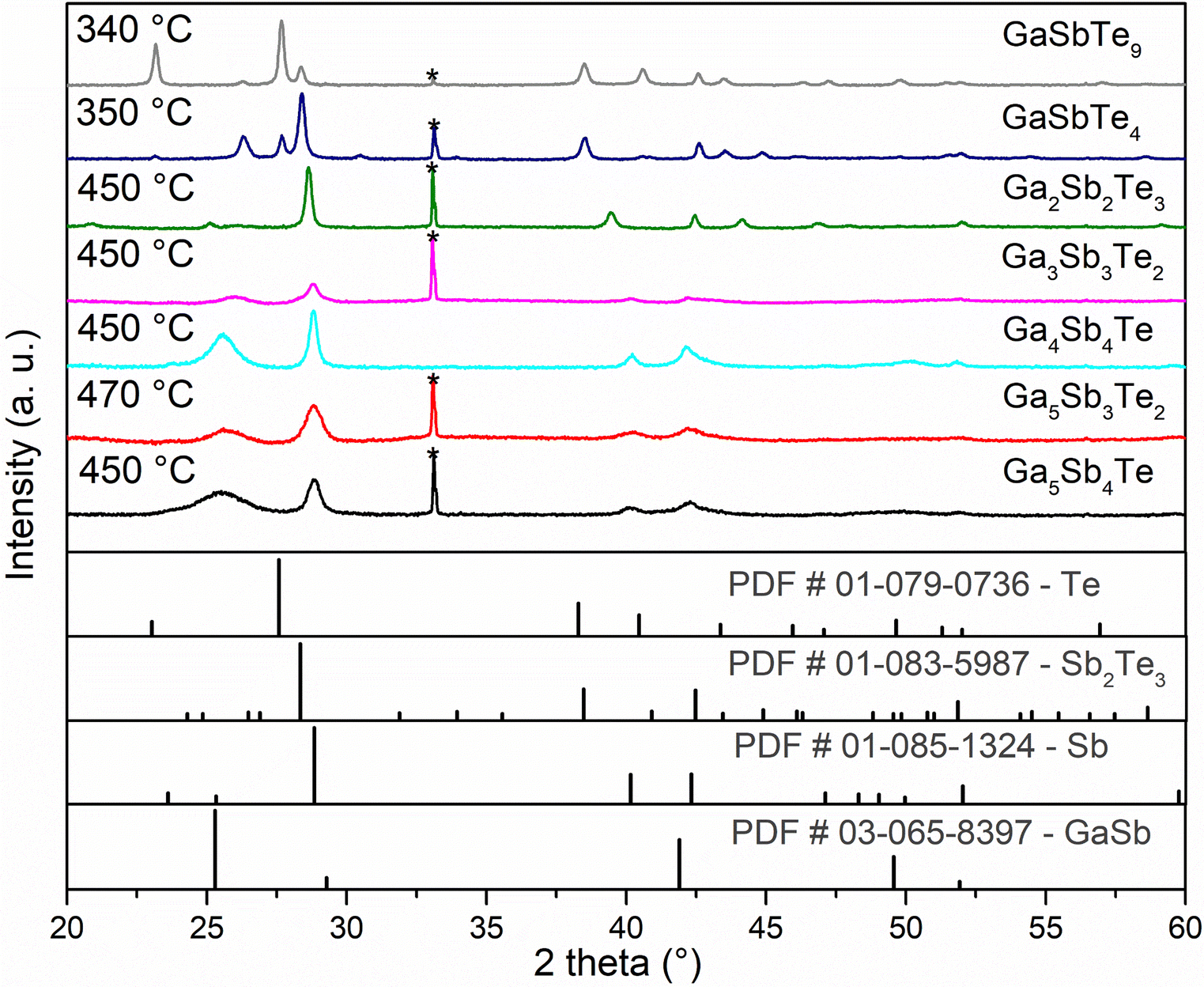 | ||
| Fig. 4 Room temperature XRD patterns of Ga–Sb–Te co-sputtered annealed films and powder diffraction patterns of the Te, Sb2Te3, Sb and GaSb from the crystallographic database;32 * refers to the peaks from the silicon substrate (100). Annealing temperature is specified for each composition. | ||
Raman scattering spectra of the studied Ga–Sb–Te thin films in both as-deposited and annealed states covering the region from 25 to 300 cm−1 are presented in Fig. 5.
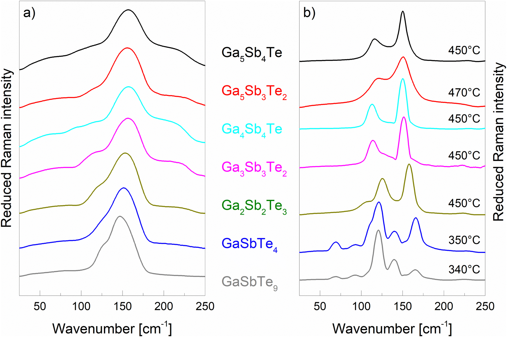 | ||
| Fig. 5 Raman scattering spectra of co-sputtered Ga–Sb–Te layers: (a) as-deposited state and (b) annealed state. Annealing temperature is specified for each composition. | ||
The measured Raman spectra of the as-deposited Ga–Sb–Te thin films with higher content of GaSb exhibit broad peaks/arms at ∼50 and ∼225 cm−1, together with the higher intensity peak at 150 cm−1. These peaks were also reported by Carles et al.33 when studying non-stoichiometric amorphous GaSb films. The reduced intensity of the Raman spectra in ref. 33 shows a peak at 150 cm−1 for the longitudinal acoustic (LA) mode of GaSb and both longitudinal (LO) and transverse (TO) optical Sb modes. The shoulder lying in the range from 190 to 230 cm−1 corresponds mainly to the LO and TO modes of GaSb.33 The same publication also mentions a peak at ∼105 cm−1 and suggests the contributions of GaSb longitudinal optical modes that are probably connected to the change in GaSb stoichiometry – the peak decreases its intensity with higher deviation from stoichiometry. As the amount of Te increases in the measured Ga–Sb–Te amorphous samples, the Raman spectra continue to exhibit the main peak with the highest maximum that slightly shifts to lower wavenumbers ∼145 cm−1 while the surrounding peaks/arms disappear – instead a new arm at ∼125 cm−1 appears. Previously studied Raman spectra of amorphous Te consist of broad maxima at 90 and 157 cm−1,34 and amorphous Sb2Te3 thin films prepared by PLD show only maxima of a broad band at 145 cm−1 assigned to Sb–Te bond vibrations.35 Therefore, the interpretation of measured amorphous data with higher content of Te might be less clear, as the peaks of the vibrations of bands of Te–Te, Sb–Te, and Sb–Sb are very close to each other and there is a high probability of peak overlapping.
Raman spectra of crystallized films show a relatively different and clearly identifiable Raman spectrum shape, with better band structuring than for amorphous films. The Raman spectra for annealed Ga–Sb–Te thin films with higher content of GaSb exhibit characteristic bands at 210–240 cm−1 that can be assigned as LO modes with the addition of TO modes of GaSb36 together with bands at 114–150 cm−1 belonging to Sb–Sb bond vibrations.33 The spectra for annealed films with less content of Te are close to those published by Carles et al.33 For annealed films with higher Te content, vibrations of Te–Te bonds at ∼92, 121, and 140 cm−1 corresponding to the three first-order Raman modes E1 (TO), A1 and E2 (TO) of Te appear.37 The band at ∼69 cm−1, the shoulder at ∼110 cm−1 and the band at ∼166 cm−1 correspond to the A1g, Eg and A1g normal modes of the Sb–Te vibrations in Sb2Te3.38,39 The presence of the above-mentioned vibrations of bonds is in accordance with the XRD results revealing Te, Sb2Te3, Sb, GaSb and gallium antimony telluride as possible phases in annealed films.
Fig. 6 illustrates the spectral dependencies of the optical functions (refractive index and extinction coefficient) for both as-deposited and annealed Ga–Sb–Te thin films. The spectral dependence of the extinction coefficient as well as refractive index for the as-deposited films has a similar shape for all compositions. The transparency range of the annealed samples is decreased due to absorption coming from a Drude-like contribution from free carriers. Ciesielski et al.40 reported a refractive index value of ∼5 for longer wavelengths (within the transparent spectral region) for the tellurium thin film with a thickness of 30 nm. In our case the optical functions’ spectral dependences as well as values of the refractive index for the annealed layers with the highest Te content (GaSbTe9 and GaSbTe4) are close to crystalline ordinary tellurium optical constants published by Palik.41 In our opinion the optical functions of GaSb42 and/or Sb43 together with Sb2Te344 also influence the optical constants of the annealed samples as all the above-mentioned phases were found from evaluation of XRD spectra. For possible practical utilization of the studied materials, the optical contrast calculated as Δn + iΔk (n, k (annealed)-n, k (as-deposited)) for a working wavelength of BD (405 nm) and absolute values of optical contrast at 405 nm in terms of |Δn| + |Δk| are of interest.45 The calculated values of optical contrast and their absolute values are shown in Table 2. The highest absolute value of optical contrast was found for Ga5Sb4Te and GaSbTe9 and it reached a value up to ∼1.85 which is comparable to Ge2Sb2Te5 (2.25).10 Spectroscopic ellipsometry also allowed determining the thickness difference between the as-deposited and annealed samples. The difference was found to be maximally 8% for the samples with a thickness ∼170 nm, which is lower than previously reported values (up to 22%) for Ga–Sb–Te layers prepared by RF magnetron co-sputtering.22
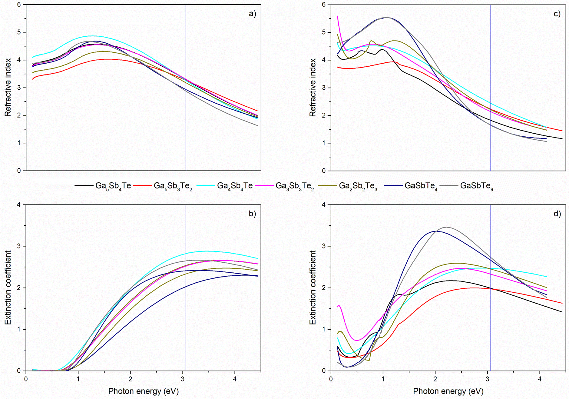 | ||
| Fig. 6 Optical functions of both as-deposited and annealed (co-)sputtered Ga–Sb–Te thin films: (a) spectral dependences of refractive indices of the as-deposited films; (b) spectral dependences of the extinction coefficients of the as-deposited films; (c) spectral dependences of the refractive indices of the annealed films; (d) spectral dependences of the extinction coefficients of the annealed films. Vertical lines represent the wavelength of 405 nm used in Blu-ray technology. | ||
Although an increase in the root mean square (RMS) surface roughness after annealing is expected measured RMS of the as-deposited as well as annealed samples obtained from AFM over 2 μm × 2 μm scans is below 0.5 nm for all samples (exemplified by Fig. 7).
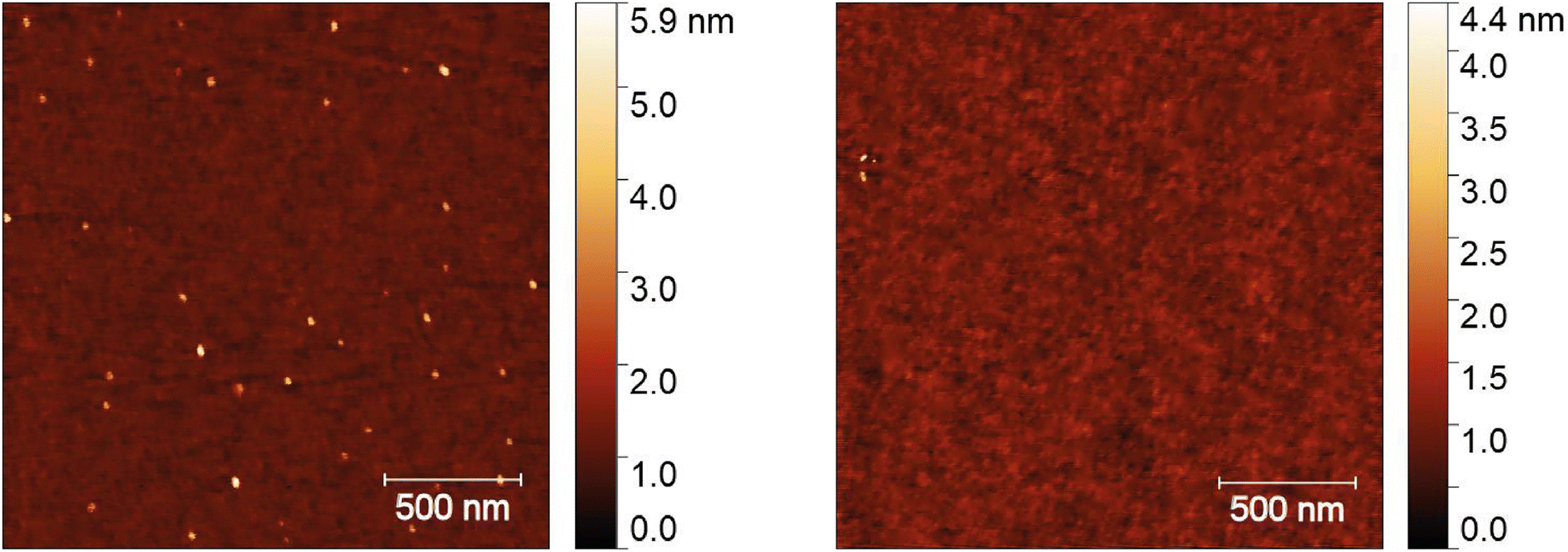 | ||
| Fig. 7 Examples of AFM scans (2 × 2 μm) for Ga5Sb3Te2: as-deposited (RMS roughness = 0.2 nm, left) and annealed to 470 °C (RMS = 0.2 nm, right). | ||
Conclusions
A study of Ga–Sb–Te phase change materials with potential application as phase-change memories was conducted, focusing on GaSb–GaTe and GaSb–Te binary tie-lines. Different properties of as-deposited (amorphous) as well as annealed (crystalline) layers were studied to shed more light on the mechanism of the phase-change in such materials. The crystallization temperatures determined from temperature-dependent sheet resistance measurement of the compositions on the GaSb–GaTe tie-line tend to decrease from 340 to 315 °C with increasing content of GaTe. On the other hand, the crystallization temperatures of the thin films from the GaSb–Te tie-line are lower and gradually decrease from 305 to 100 °C with increasing content of Te. The crystallization temperature obtained from temperature-dependent sheet resistance measurement is in good agreement with that obtained from temperature dependent X-ray diffraction. The surface roughness obtained from AFM is below 0.5 nm for the as-deposited as well as annealed samples.Besides the drop in electrical resistivity (∼4–7 orders of magnitude), there is also a clear change in optical functions upon crystallization. The highest values of |Δn| + |Δk| equal to 1.83 and 1.85 for a wavelength of 405 nm were determined for Ga5Sb4Te and GaSbTe9 thin films which are comparable with the value for Ge2Sb2Te5 used in commercial rewritable optical storage discs (CD-RWs, Blu-ray).
X-Ray diffraction revealed the presence of the following possible phases in annealed films: Sb, GaSb, gallium antimony telluride together with Sb2Te3 and Te. Additionally, Raman spectra revealed the vibrational modes of Ga–Sb bonds, vibrations of Sb–Sb bonds, vibrations of Te–Te bonds and vibrations of Sb–Te bonds.
To conclude, the compositions suitable for further studies seem to be Ga5Sb4Te and Ga5Sb3Te2. Their main characterization was the stability of the material, good optical contrast (in the case of Ga5Sb4Te) and satisfying electrical contrast. On the other hand, the downside of these samples is the higher Tc.
Author contributions
MK & PJ: ellipsometric data measurements/data treatment, draft writing; JG & TH: thin film depositions; JP: resistivity measurements, SŠ: EDS, SEM; VN: Raman spectra measurements, draft reviewing and editing; FC: TD-XRD; PN: supervision, funding, draft reviewing and editing.Conflicts of interest
There are no conflicts to declare.Acknowledgements
The financial support from the Czech Science Foundation (GA ČR), project No. 22-07635S is highly appreciated. This work was also supported by the Ministry of Education, Youth, and Sports of the Czech Republic, grant number LM2023037. Raman spectroscopy measurements were conducted by Platform SIR of ScanMAT UAR 2025 CNRS at Rennes University.References
- S. Raoux, F. Xiong, M. Wuttig and E. Pop, MRS Bull., 2014, 39, 703–710 CrossRef.
- R. Waser, Nanoelectronics and Information Technology: Advanced Electronic Materials and Novel Devices, John Wiley & Sons, Berlin, 2012 Search PubMed.
- M. H. R. Lankhorst, L. van Pieterson, M. van Schijndel, B. A. J. Jacobs and J. C. N. Rijpers, Jpn. J. Appl. Phys., 2003, 42, 863–868 CrossRef CAS.
- D. Lencer, M. Salinga, B. Grabowski, T. Hickel, J. Neugebauer and M. Wuttig, Nat. Mater., 2008, 7, 972–977 CrossRef CAS PubMed.
- C. Peng, L. Wu, F. Rao, Z. Song, P. Yang, L. Cheng, J. Li, X. Zhou, M. Zhu, B. Liu and J. Chu, ECS Solid State Lett., 2012, 1, P38 CrossRef CAS.
- Y. Wang, Y. Zheng, G. Liu, T. Li, T. Guo, Y. Cheng, S. Lv, S. Song, K. Ren and Z. Song, Appl. Phys. Lett., 2018, 112, 133104 CrossRef.
- Y. Lai, B. Qiao, J. Feng, Y. Ling, L. Lai, Y. Lin, T. Tang, B. Cai and B. Chen, J. Electron. Mater., 2005, 34, 176–181 CrossRef CAS.
- K. B. Borisenko, Y. Chen, D. J. H. Cockayne, S. A. Song and H. S. Jeong, Acta Mater., 2011, 59, 4335–4342 CrossRef CAS.
- Q. Wang, B. Liu, Y. Xia, Y. Zheng, R. Huo, Q. Zhang, S. Song, Y. Cheng, Z. Song and S. Feng, Appl. Phys. Lett., 2015, 107, 222101 CrossRef.
- N. Yamada, Phys. Status Solidi B, 2012, 249, 1837–1842 CrossRef CAS.
- M. Bouška, V. Nazabal, J. Gutwirth, T. Halenkovič and P. Nemec, J. Non-Cryst. Solids, 2021, 569, 121003 CrossRef.
- K. Kurata and T. Hirai, Solid-State Electron., 1966, 9, 633–640 CrossRef CAS.
- C.-M. Lee, Y.-I. Lin and T.-S. Chin, J. Mater. Res., 2004, 19, 2929–2937 CrossRef CAS.
- C.-M. Lee, Y.-I. Lin and T.-S. Chin, J. Mater. Res., 2004, 19, 2938–2946 CrossRef CAS.
- H.-Y. Cheng, S. Raoux and J. L. Jordan-Sweet, Appl. Phys. Lett., 2011, 98, 121911 CrossRef.
- Y. Lu, S. Song, Z. Song, W. Ren, Y. Cheng and B. Liu, Appl. Phys. Express, 2011, 4, 094102 CrossRef.
- J. Cui, X. Liu, W. Yang, D. Chen, H. Fu and P. Ying, J. Appl. Phys., 2009, 105, 063703 CrossRef.
- K.-F. Kao, C.-M. Lee, M.-J. Chen, M.-J. Tsai and T.-S. Chin, Adv. Mater., 2009, 21, 1695–1699 CrossRef CAS.
- K.-F. Kao, C.-C. Chang, F. T. Chen, M.-J. Tsai and T.-S. Chin, Scr. Mater., 2010, 63, 855–858 CrossRef CAS.
- A. T. H. Chuang, Y.-C. Chen, Y.-C. Chu, P.-C. Chang, K.-F. Kao, C.-C. Chang, K.-Y. Hsieh, T.-S. Chin and C.-Y. Lu, in 2011 3rd IEEE International Memory Workshop (IMW), 2011, pp. 1–3.
- K.-F. Kao, Y.-C. Chu, M.-J. Tsai and T.-S. Chin, J. Appl. Phys., 2012, 111, 102808 CrossRef.
- M. Bouška, V. Nazabal, J. Gutwirth, T. Halenkovič, J. Přikryl, S. Normani and P. Němec, Opt. Lett., 2020, 45, 1067–1070 CrossRef PubMed.
- C.-M. Lee, W.-S. Yen, J.-P. Chen and T.-S. Chin, IEEE Trans. Magn., 2005, 41, 1022–1024 CAS.
- X. W. Zhou, D. K. Ward, F. P. Doty, J. A. Zimmerman, B. M. Wong, J. L. Cruz-Campa, G. N. Nielson, J. J. Chavez, D. Zubia and J. C. McClure, Prog. Photovolt. Res. Appl., 2015, 23, 1837–1846 CrossRef CAS.
- T.-Y. Lai, T.-H. Fang and T.-H. Chen, Phys. E, 2020, 124, 114300 CrossRef CAS.
- A. Bouzid, S. Gabardi, C. Massobrio, M. Boero and M. Bernasconi, Phys. Rev. B: Condens. Matter Mater. Phys., 2015, 91, 184201 CrossRef.
- H.-Y. Cheng, K.-F. Kao, C.-M. Lee and T.-S. Chin, IEEE Trans. Magn., 2007, 43, 927–929 CAS.
- J. Gutwirth, M. Kotrla, T. Halenkovič, V. Nazabal and P. Němec, Nanomaterials, 2022, 12, 1830 CrossRef CAS PubMed.
- G. D. Cody, in Semiconductors and Semimetals, ed. J. I. Pankove, Academic Press, Orlando, 1st edn, 1984, pp. 11–82 Search PubMed.
- L. J. van der Pauw, Philips Res. Rep., 1958, 13, 1–9 Search PubMed.
- R. Shuker and R. W. Gammon, Phys. Rev. Lett., 1970, 25, 222–225 CrossRef CAS.
- S. Gates-Rector and T. Blanton, Powder Diffr., 2019, 34, 352–360 CrossRef CAS.
- R. Carles, J. B. Renucci, A. Gheorghi and M.-L. Theye, Philos. Mag. B, 1984, 49, 63–71 CAS.
- M. H. Brodsky, R. J. Gambino, J. E. Smith Jr. and Y. Yacoby, Phys. Status Solidi B, 1972, 52, 609–614 CrossRef CAS.
- P. Nemec, V. Nazabal, A. Moréac, J. Gutwirth, L. Benes and M. Frumar, Mater. Chem. Phys., 2012, 136, 935–941 CrossRef CAS.
- J. H. Dias da Silva, S. W. da Silva and J. C. Galzerani, J. Appl. Phys., 1995, 77, 4044–4048 CrossRef.
- A. S. Pine and G. Dresselhaus, Phys. Rev. B: Solid State, 1971, 4, 356–371 CrossRef.
- W. Richter, J. Phys. Chem. Solids, 1972, 33, 2123–2128 CrossRef CAS.
- G. C. Sosso, S. Caravati and M. Bernasconi, J. Phys.: Condens. Matter, 2009, 21, 095410 CrossRef CAS PubMed.
- A. Ciesielski, Ł. Skowroński, W. Pacuski and T. Szoplik, Mater. Sci. Semicond. Process., 2018, 81, 64–67 CrossRef CAS.
- E. D. Palik, in Handbook of Optical Constants of Solids, ed. E. D. Palik, Academic Press, Boston, 1998, pp. 709–723 Search PubMed.
- D. E. Aspnes and A. A. Studna, Phys. Rev. B: Condens. Matter Mater. Phys., 1983, 27, 985–1009 CrossRef CAS.
- T. J. Fox, R. P. Howson and D. C. Emmony, J. Phys. Appl. Phys., 1974, 7, 1864 CrossRef CAS.
- P. Nemec, J. Prikryl, V. Nazabal and M. Frumar, J. Appl. Phys., 2011, 109, 073520 CrossRef.
- N. Yamada, R. Kojima, T. Nishihara, A. Tsuchino, Y. Tomekawa and H. Kusada, Proc. E* PCOS, 2009, 2009, 23–28 Search PubMed.
Footnote |
| † Electronic supplementary information (ESI) available. See DOI: https://doi.org/10.1039/d4ma00049h |
| This journal is © The Royal Society of Chemistry 2024 |