
 Open Access Article
 This Open Access Article is licensed under a Creative Commons Attribution-Non Commercial 3.0 Unported Licence
High on/off ratio SiO2-based memristors for neuromorphic computing: understanding the switching mechanisms through theoretical and electrochemical aspects†
Fei
Qin‡
a,
Yuxuan
Zhang‡
a,
Ziqi
Guo
b,
Tae Joon
Park
c,
Hongsik
Park
 d,
Chung Soo
Kim
e,
Jeongmin
Park
e,
Xingyu
Fu
a,
Kwangsoo
No
f,
Han Wook
Song
g,
Xiulin
Ruan
b and
Sunghwan
Lee
*a
d,
Chung Soo
Kim
e,
Jeongmin
Park
e,
Xingyu
Fu
a,
Kwangsoo
No
f,
Han Wook
Song
g,
Xiulin
Ruan
b and
Sunghwan
Lee
*a
aSchool of Engineering Technology, Purdue University, West Lafayette, IN 47907, USA. E-mail: sunghlee@purdue.edu
bSchool of Mechanical Engineering, Purdue University, West Lafayette, IN 47907, USA
cSchool of Materials Engineering, Purdue University, West Lafayette, IN 47907, USA
dSchool of Electronic and Electrical Engineering, Kyungpook National University, Daegu 41566, Republic of Korea
eAnalysis Technical Center, Korea Institute of Ceramic Engineering and Technology, Jinju, Gyeongsangnam-do 52851, Republic of Korea
fDepartment of Materials Science and Engineering, KAIST, Daejeon 34141, Republic of Korea
gCenter for Mass and Related Quantities, Korea Research Institute of Standard and Science, Daejeon 34113, Republic of Korea
First published on 1st April 2024
Abstract
Memristors have emerged as promising elements for brain-inspired computing applications, yet the understanding of their switching mechanisms, particularly in valence change memristors, remains a topic of ongoing debate. We report on the SiO2-based memristors, demonstrating a high on/off ratio (>105). Particularly, this study aims to enhance the fundamental understanding of switching behaviors and mechanisms. Our approach involved an extensive investigation using finite element analysis to provide visual insights into the conductive path evolution in these memristors over the set/reset bias cycle. Electrochemical impedance spectroscopy experimentally validated the theoretical investigations by interpreting the switching behavior through the lens of the equivalent circuit. In addition, we evaluated synaptic characteristics and incorporated them into neural networks for image recognition tasks with MNIST and fashion MNIST datasets. Our comprehensive exploration of both the underlying principles and potential applications is of practical relevance to studies that aim to realize and implement SiO2-based memristors in neuromorphic computing.
Introduction
The silicon (Si) microelectronics research and industry promisingly consider memristors a promising contender in emerging memory technologies. This increasing interest in memristors is attributed to their potential performance advantages, including lower power consumption and higher scalability, compared with other non-volatile memory technologies such as FeRAM (ferroelectric RAM) and MRAM (magnetoresistive RAM).1 These distinct characteristics of memristors position them as a compelling choice for implementing in-memory computing, offering a path to challenge and potentially revolutionize traditional Von Neumann architectures.A wide range of oxide materials, from semiconductors to high-k materials, including InGaZnO,2 SiO2,3 HfO2,4 and TaOx,5 have been reported to serve as switching layers in memristors. The majority of materials utilized in memristors are either expensive to grow or only partially compatible with the prevalent Si-based complementary metal–oxide semiconductor (CMOS) manufacturing process. Historically, SiO2 has been one of the most extensively researched dielectric materials, largely due to its direct growth capability out of Si.6 However, much of this research has been centered around the destructive and irreversible dielectric breakdown for traditional CMOS and very large-scale integration (VLSI) technologies.7 Recently, a shift in focus has been noted within the memristor field, as SiO2 has demonstrated reversible soft breakdown behaviors, also known as resistive switching.3,8 This has prompted an increase in interest and research into the potential applications of SiO2 within the realm of memristor technologies.9
Memristors based on SiO2 have been investigated and reported with an achieved performance of on/off ratio of 102–105.8b,10 Bilayer structure (SrTiO3/SiO211) was demonstrated for realizing stable switching through engineering different ion transport rates in these two layers where the role of SrTiO3 is to confine filament growth. Nanorods of SiO2 were also investigated to lower the firing energy for an artificial neuron.12 The use of columnar growth in silicon oxide was leveraged to create defect-rich sites at the column edges, resulting in low variability.10b To further advance the development, it is crucial to fundamentally understand SiO2-based memristors’ switching mechanisms, which in turn will provide insightful engineering criteria to address the challenging issues above. Thus far, the oxidation-reduction (redox)-based switching mechanisms have been suggested and categorized into two mechanisms, depending on the composition of the conductive filaments: electrochemical metallization mechanism (ECM) and vacancy-associated valence change mechanism (VCM). In an ECM device, Cu or Ag is widely chosen as an active electrode which can be partially oxidized and then reduced to form the metallic filaments.13 On the other hand, the conductive path of VCM devices relies on the generation and accumulation of oxygen vacancies.14 The evolution of conductive filaments in the ECM memristors has been evidenced through transmission electron microscopy (TEM),15 and this work enhanced understanding of the switching behavior of ECM and PCM memristors.14 However, the direct visualization of conductive filaments in VCM-based memristors is rarely reported due to the technical difficulties,16 for example in TEM characterizations, of low image contrast between oxygen-rich and -deficient regions in TEM characterizations, which makes the VCM switching mechanism remain controversial.17
In this work, we selected SiO2 as the switching element for memristor applications. To solely limit the contributing charge carriers to oxygen vacancies for the switching behavior, an inert metal Pd was employed as the top electrode. The dynamic evolution of oxygen vacancy conductive filaments in the SiO2-based memristors was mechanistically visualized by a numerical solver, which delineates a selective growth process and the inhibition effect exerted on filaments nearby the established dominant paths. The equivalent circuit interpretation from non-destructive electrochemical impedance spectroscopy (EIS) measurements supplementarily corroborated our theoretical understanding about the switching mechanism. Importantly, our SiO2-based memristor can be considered as the weights in artificial neural networks (ANNs) because it exhibited multi-conductance phenomena in response to pulse train stimuli. Given these synaptic characteristics, our SiO2-based memristors were incorporated into a neural network for image processing tasks, benchmarking with MNIST and fashion MNIST datasets. Our fundamental studies and concept validation may propel advances in SiO2-based memristors, pushing the boundaries towards real-world neuromorphic computing applications.
Results and discussion
Fig. 1a is a schematic illustration of a SiO2-based memristor in a vertical configuration. The top electrodes were defined using in situ shadow masks during the fabrication, of which the circular pattern diameters vary from 150 to 300 μm with a 50 μm increment. A cross-sectional high-angle-annular dark-field (HAADF) TEM micrograph of the SiO2 memristor is false-colored and exhibited in Fig. 1b. A vertical memristor structure consisting of top (Pd, ∼100 nm) and bottom (heavily-doped Si) electrodes and switching layer (SiO2, ∼20 nm) between the electrodes was clearly identified. An associated energy-dispersive X-ray spectroscopy (EDS) mapping image in Fig. 1b indicates the major elements of each layer of the memristor, indicating a clear interface between layers without interdiffusion. In the high-resolution TEM images (Fig. 1c), distinct morphological features are evident: the TE/SiO2 interface exhibits protrusions approximately 1 nm in size (Fig. 1c1), while the SiO2/BE interface is characterized by a notably flat surface (Fig. 1c2). A false-colored SEM image of the Pd top electrodes with diameters of 200 and 150 μm is displayed in Fig. 1d and a magnified image of a 150 μm Pd top electrode is shown in Fig. 1e. The typical vertical memristor structure is technically the same as that of a capacitor and particularly the characteristics of the high-resistance state are governed by the dielectric performance of the switching layer (SiO2 in this study). To evaluate the dielectric property, as an initial figure of merit, of the switching layer and the devices, capacitance–voltage (CV) measurements were conducted on SiO2-based memristors as a function of switching layer thicknesses and top electrode size within a voltage range from −2 V to 2 V under 1 MHz. The CV results from the 5 nm SiO2 switching layer are summarized in Fig. 1f. Overall, the capacitance of 5 nm SiO2-based memristors is at 10−10 F level. From the C–V measurements, the capacitance densities of the SiO2 switching layers with different TE sizes are comparable to each other, approximately 3.5–4.2 fF μm−2. The relative permittivity extracted from the resulting sputtered SiO2 is 3.3, which is close to the reference values 3.7–3.9.18 The slightly lower value may be resulted from the room temperature sputtering condition and mild annealing temperature (550 °C), compared with the reference values obtained from high temperature (1000–1200 °C) thermal oxidation.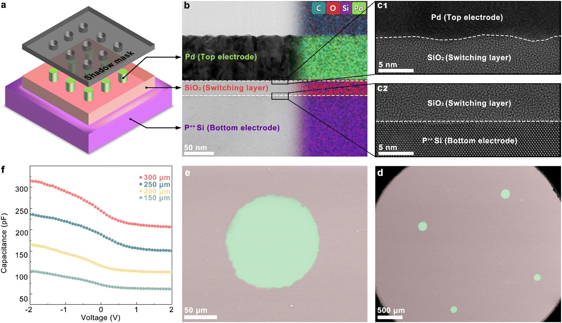 | ||
| Fig. 1 Pd/SiO2/P++Si memristors: (a) schematic illustration of device structure of SiO2-based memristor with Pd TE and heavily-doped Si BE. (b) A false-colored cross-sectional HAADF-TEM micrograph, and associated EDS elemental mapping of a Pd/SiO2/P++Si memristor. (c) High resolution TEM images to reveal the morphology of (c1) the TE/SiO2 interface, showing ∼1 nm protrusions and (c2) the flat SiO2/BE interface. (d) A false-colored SEM plan-view image of the top electrodes with diameters of 200 μm and 150 μm, and (e) an extended image for the typical size 150 μm. (f) C–V measurements at 1 MHz for 5 nm-thick SiO2-based memristor with various TE diameters (300, 250, 200 and 150 μm). | ||
The electrical characteristics of SiO2-based memristors were examined by cyclic DC sweeping. The electrical biases were always applied on the palladium top electrode and the P++ Si bottom electrode was grounded. The sweeping bias ranged from −5 V to 7.5 V with a starting voltage of 0 V, and a compliance current (Icc) was set at 60 μA during the positive sweeping. Fig. 2a shows the current–voltage (I–V) property of a 5 nm-SiO2 switching layer memristor, including consecutive 100 cycles of DC sweeping curves with the same measurement parameters. The I–V sweeping curves appear as a butterfly shape which is a typical pattern for a bipolar memristor.21 The bipolar switching resulted from the formation (with positive biases) and annihilation (with negative biases) of the filament, caused by field induced oxygen vacancy migration with alternating opposite directions of bias application.19 This is different from the unipolar switching which has been proposed, where the annihilation of the filament is achieved by Joule heating using a consistent bias direction.20 When the bias increased from 0 V to 7.5 V, abrupt current jumps were observed which indicates a conduction filamentary SET process, i.e., a transition from high resistance state (HRS) to low resistance state (LRS). And the transitions (turn on) mostly happened at a voltage ranging from 4 V to 6 V. The LRS was maintained during the sweeping from 7.5 V to 0 V and subsequent 0 V to negative bias. It should be noted that the turn-on voltage of the first cycle of DC sweeping was ∼6 V which was applied on the top electrode (Pd). From the SET voltage statistics distribution in Fig. 2f (bottom for 5 nm thick SiO2), it is on the maximum side, but not too far from the medium/mean value of ∼5 V. Thus, we can consider our device to be a near-forming free device, which is defined as the initial SET voltage of the device is similar to the subsequent SET voltages.21 During the negative voltage sweeping, a current level drop was observed which means the cell was turned back to HRS, a RESET process was finished (i.e., off state). The current values at a read voltage of 0.3 V for each sweeping cycle were extracted from the I–V curves, then converted to resistance values and plotted as resistance versus cycle number to yield the endurance performance of the device exhibited in Fig. 2b. The results demonstrate that no deterioration in HRS and LRS during continuous cycling was observed, indicating reasonable endurance of the SiO2-based memristor. A large memory window, i.e., on/off ratio, is clearly observed as high as >105. To characterize the on/off ratio more quantitatively, the cycle-to-cycle statistical distributions of HRS and LRS are demonstrated in Fig. 2c. At the cumulative probability of 50%, the notable high on/off ratio is further validated as ∼1.4 × 10⁵. The achieved high on/off ratios are attributed to the low off-state current and the high on-state current. The low off-state current behavior mainly depends on the intrinsic quality of the switching layer (i.e., dielectric property). As the capacitance–voltage characteristics are provided in Fig. 1f, our sputter-processed SiO2, followed by air annealing, demonstrates decent dielectric performance, comparable (or slightly less) to bulk and thermally grown SiO2. Therefore, our SiO2-based memristor achieved an off-sate current as low as on the order of 10−11–10−10 A. For the on-state behavior, various parameters are related to the overall on-state property, such as the intrinsic characteristics of the switching layer, thickness, and the transport behavior of the charged carriers (oxygen vacancy in this case), and hence the resulting conductivity of the filament. In addition to these intrinsic and processing parameters of the materials and device, a measurement parameter of the compliance current (Icc) is also an important factor in determining the on/off ratio, as it limits the maximum current flowing through the device. This not only prevents the device from experiencing a hard breakdown but is also proposed to control filament growth.22 With Icc = 60 μA in our study, the conduction filament, once formed, has sufficient conductivity (Fig. S1 in the ESI†) to achieve a relatively high on-current, thereby exhibiting resistive behavior. Furthermore, the regulated filament can be near-fully ruptured during the RESET process to get the low current again, contributing to the high on/off ratio.23 To assess the stability of our device, the retention characteristics were evaluated with a read voltage 0.3 V at an evaluated temperature 85 °C. As depicted in Fig. 2d, both the LRS and HRS show a prolonged retention time of 104 seconds. In regard to the device-to-device variation, all the processing parameters and annealing environment are carefully controlled and monitored for the processing of our SiO2 memristors, to minimize any processing variations and hence the possible performance variations. The performance of our SiO2-based memristors slightly varies among the devices and particularly the on/off ratio is found to be reasonably consistent as shown in Fig. 2e, demonstrating 0.9–1.6 × 10⁵. Additionally, the SET voltage exhibits very small device-to-device variation of 2.90% (Fig. S2, ESI†). This device-to-device evidence, in conjunction with previous cycle-to-cycle tests, underscores the reasonable reliability of our devices. To evaluate the effect of the thickness of the SiO2 layer, similar electrical characterizations were also carried out on 10 nm, 20 nm, and 30 nm SiO2 switching layer memristors. The I–V characteristics for these switching layer thicknesses can be found in Fig. S3 (ESI†). It is observable that devices with thicker switching layers require a higher voltage for stable resistive switching. The SET voltages are statistically summarized in Fig. 2f. A clear quantitative trend is confirmed, indicating that SET voltage increases with the thickness of the switching layer. The difference in SET voltage between the 5 nm and 30 nm SiO2 devices is approximately 9 V. From a practical perspective, thinner SiO2-based memristors offer higher energy efficiency. Fig. 2g compares the on/off ratio of the present study with those available in the literature. For objective comparisons, the other two widely-considered oxides of TaOx (as Work 4,24 5,25 and 626) and HfOx (as Work 7,27 8,28 and 929) are also included in Fig. 2g as well as SiOx (as Work 1,10e 2,30 and 331). The achieved on/off ratio of >105 from our SiO2 memristors outperforms those (∼101–104) of state-of-the-art HfOx- and TaOx-based memristors. In addition to the on/off performance, the unit price of these switching materials is also compared. Due to the abundance, SiO2 is significantly cost-effective (100–700 times lower) than the other competitors.32 In order to make our comparison more comprehensive, we compared the endurance and retention in our work with those in other literature. The comparisons are presented in Table S1 (ESI†), where our device exhibits reasonable reliability, in terms of both endurance and retention, demonstrating on the order of 102 cycles and 104 s.
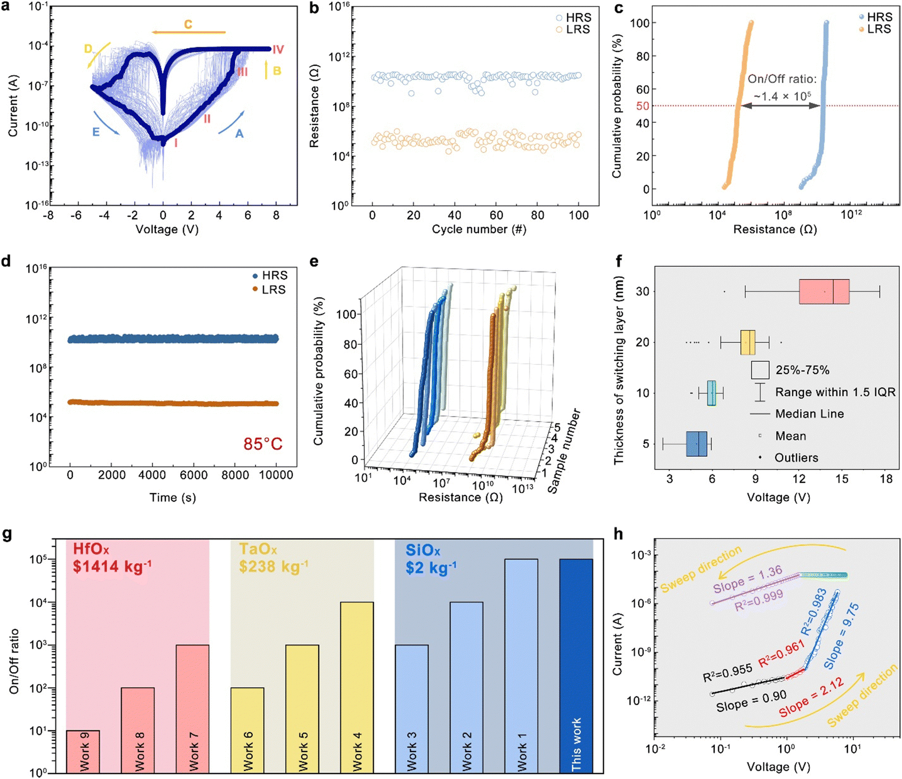 | ||
| Fig. 2 (a) I–V characteristics of the Pd/SiO2 (5 nm)/P++-Si memristor in semi-log scale, where arrows, labeled in alphabetical order, indicate HRS, SET, LRS, RESET, and HRS, respectively. (b) Endurance graph for 100 cycles, two distinct HRS and LRS remain without damping. The resistance values at HRS and LRS are recorded at a read voltage of 0.3 V. (c) Statistical distribution of resistance at HRS and LRS, from which the on/off ratio is extracted to be ∼1.4 × 10⁵ at a cumulative possibility of 50%. (d) The retention characteristics of 5 nm SiO2 memristor at LRS and HRS, examined at 85 °C, exhibit reasonably good performance. (e) The statistical distribution of RHRS and RLRS for 5 different devices. The on/off ratios were obtained by using the same method in (b). Similar high on/off ratios of ∼105 are obtained from all the devices. (f) Statistical distribution SET voltages for different thicknesses of SiO2 switching layers. (g) Comparison of the on/off ratio of the present study with those from the literature. (h) Analysis of electric transport processes of the SiO2-based memristor in log–log scale. | ||
To analyze electric transport processes, the linear scale I–V curve in Fig. 4a was replotted in double-log scale in Fig. 2h to examine the power law behavior between the current and voltage (i.e., I ∝ Vm). During the HRS, the curve exhibits three regimes where m ≈ 1, m ≈ 2, m > 2, representing ohmic, trap-unfilled (Child's square law), and trap-filled regimes, respectively, according to the well-known space-charge-limited conduction (SCLC) mechanism, describing the electric conduction process in a memristor.14 During the LRS, the linear fitting slope is close to one with a R2 = 0.999, indicating the ohmic conduction mechanism (Fig. S4 shows other conduction mechanisms exhibit inferior fits, ESI†), which is widely considered to be attributed to the formation of a conductive filament bridging the TE and BE in a metallic-like way.33 Additionally, our area effect study in Fig. S5 (ESI†) shows that the current levels in the LRS do not significantly vary with the size of the electrode, suggesting the presence of filamentary conduction.10e,34 And the results in Fig. S6 (ESI†) for the temperature effect investigation show that the resistance values increase along with the increase in temperature, a metallic characteristic, indicating the filament is established at LRS.35 These electric transport, area effect, and temperature effect studies synergistically support that our SiO2-based memristors depend on the filamentary switching mechanism, which is further validated by the FEA (Fig. 2) and EIS (Fig. 4c) investigations in our study.
In order to enhance the fundamentals of the switching process through the evolution and rupture of an oxygen vacancy-based conduction filament as well as to complement the macroscale electrical and electrochemical measurements, we performed a series of FEA analyses as a function of applied bias. The physical modeling details are elaborated in Note S1 (ESI†). It should be noted that the switching behavior of the memristor in this study is governed by oxygen vacancies (i.e., VCM) due to the inert Pd (TE) and stably covalent-bonded Si (BE), which indicates that no electrode-related ions are involved in the conduction. A Multiphysics-fields coupled model, which describes the diffusion and drift flux of the  at the nanoscale, was adopted to study the switching process of the memristor. Several protrusions at the top electrode with various radii (r1 = 0.3 nm, r2 = 1.2 nm) were considered to reflect the roughness of the TE/SiO2 interface (Fig. 1c1). There is no chemical or structural difference between protrusions and top electrode Pd. In the left of Fig. 3a–d, the overall intensity of nD/nD0 (concentration ratio of
  at current stage to
  at original stage) gradually increased from stage I to stage IV over the course of SET process, indicating the concentration of
  was augmented in the turn-on process with increasing bias. Compared with the flat region and small protrusions on the top electrode, the protrusions with the larger radius have higher concentrations of
  , and exhibit a higher intensity of nD/nD0, which suggests that the
  is preferentially concentrated at larger protrusions. This concentration difference can be explained by the variation in the electric field, induced by the intrinsic roughness of the TE/SiO2 interface. The significantly enhanced localized electric field under the large protrusion, as confirmed in the middle of Fig. 3a–d, tends to attract more
  to regions under the protrusions with larger radius.36 Thus, our FEA analysis indicates that the selectively distributed
  may limit the random growth of the conduction filaments. This provides an insight for engineering memristors that implementing well defined protrusions may mitigate the issue regarding performance variation of memristors. The bright regions under larger protrusions at stage IV became redder and wider compared with stage III, which implies that the formed conduction filament would grow thicker. Associated schematics at each stage that elaborate the SET process are also shown on the right of our simulation results. When a positive bias is applied to the Pd TE, oxygen ions (O2−) are pulled away from the switching matrix by the external field, migrating towards the Pd TE.37 This leads to the simultaneous generation of positively charged oxygen vacancies
  . In general, this process is often described by the motion of the corresponding oxygen vacancies, i.e., the positively charged oxygen vacancies migrate towards the grounding BE and subsequently accumulate there, forming a conductive filament that bridges the TE and BE.38 Upon arriving at the Pd TE, the oxygen ions are oxidized to O2 and accumulate around the TE/SiO2 interface.17a,39 The models with different thicknesses of the switching layer were simulated as well (Fig. S7–S9, ESI†). The calculated results are consistent with the model with the SiO2 layer of 5 nm except for the turn-on voltage applied to the top electrode was increased which was led by the thicker SiO2 layer in the models.
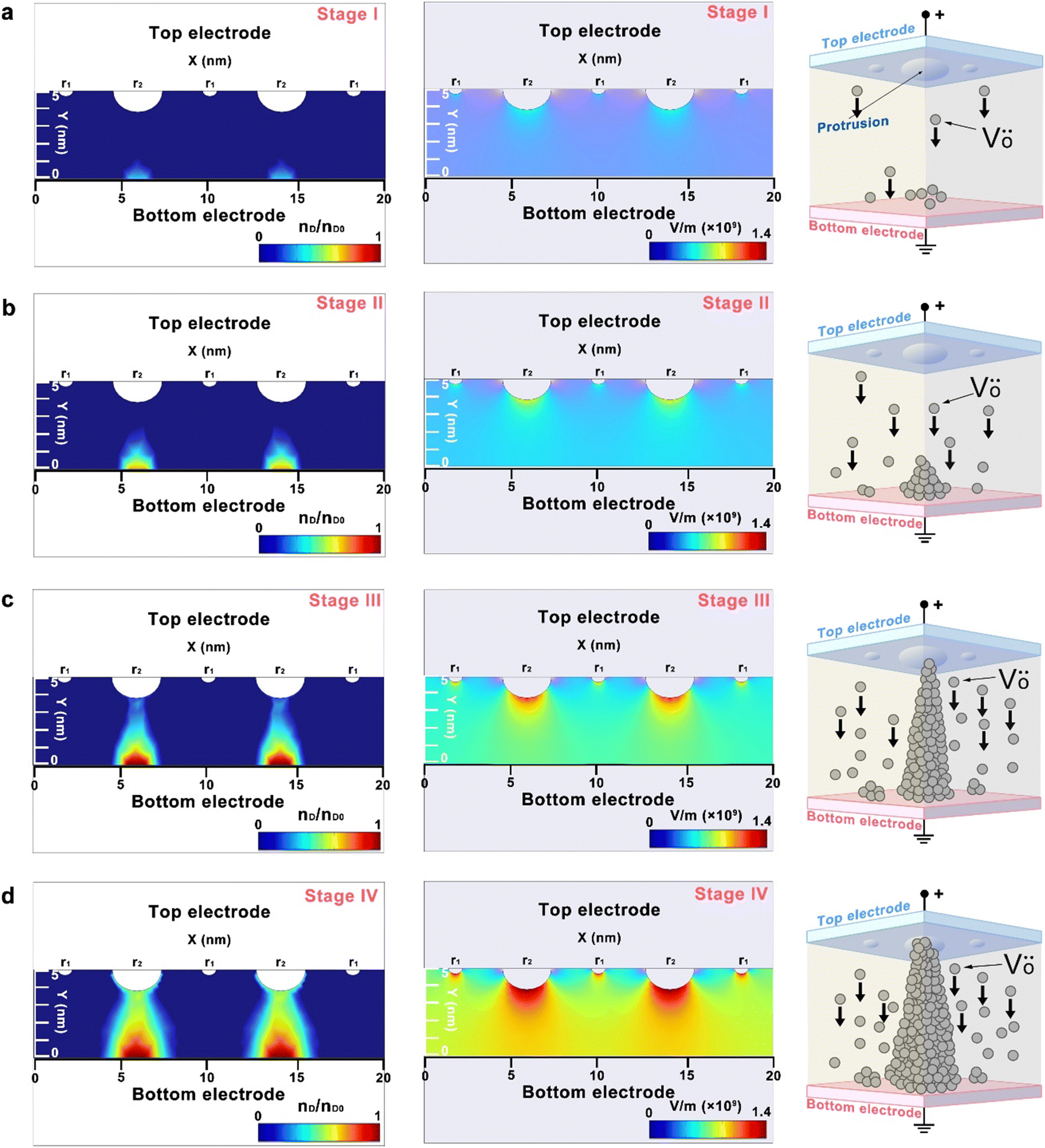 | ||
Fig. 3 The FEA visualization and schematic elaboration for the evolution of conductive filaments at (a) stage I, where small positive bias for DC sweeping is initially introduced on TE of the device, positively charged oxygen vacancies  are migrating towards BE; (b) stage II, where the magnitude of sweeping DC voltage is increasing, oxygen vacancies start accumulating at BE; (c) stage III, with voltage increasing continuously, the conductive filaments are growing; (d) stage IV, after a SET voltage applied, the conductive filaments are connecting the bottom and top electrodes, where the protrusion radii are r1 = 0.3 nm, r2 = 1.2 nm. are migrating towards BE; (b) stage II, where the magnitude of sweeping DC voltage is increasing, oxygen vacancies start accumulating at BE; (c) stage III, with voltage increasing continuously, the conductive filaments are growing; (d) stage IV, after a SET voltage applied, the conductive filaments are connecting the bottom and top electrodes, where the protrusion radii are r1 = 0.3 nm, r2 = 1.2 nm. | ||
EIS is instrumental in acquiring a deeper understanding of the fundamental electrochemical mechanisms through the evaluation of impedance variations at various sinusoidal frequencies and resulting equivalent circuit interpretation.40 Since redox-based memristors’ switching behaviors are reliant on electrochemical reactions, this non-invasive EIS technique provides a unique way to characterize and perceive memristors’ switching behavior.40b,41 Thus, the EIS measurement was carried out on SiO2-based memristors. To directly interpret the EIS results on an associated equivalent circuit model, the I–V characteristics of memristors (5 nm SiO2) were rearranged on a linear–linear scale in Fig. 4a. The green part of Fig. 4a shows I–V characteristics in a linear–linear scale for the initial high resistance state of the memristor. The EIS measurement was employed on the memristor at this state. And the resulting Nyquist plot (left; green) in Fig. 4b, exhibiting a straight line (parallel to the y-axis) supports the capacitive property of HRS of memristors. Based on the simulation, the equivalent circuit at this state consists of a resistor Rc at 102 Ω level and a capacitor Cs at 10−10 F level, connected in series. The resistance at this state of the resistor is attributed to contact resistance.42 The capacitance value is aligned with our CV measurement from pristine devices (Fig. 1f). And this capacitive property at the “initial state” is conceptually explained in the right part of Fig. 4a: the structure of a memristor at the initial state is the same as that of a capacitor and there are few native oxygen vacancies in the SiO2 switching layer. After turning on the memristor, i.e., at the state of Fig. 4a in the orange color period, an EIS measurement was repeated on the SiO2-based memristor to understand the on-state conduction behavior of the memristor. A clear semicircle in the Nyquist plot is observed in Fig. 4c (middle; orange). Compared to the equivalent circuit at the initial state, a new resistor (Rf) at 105 Ω level appears in the equivalent circuit at LRS, and it is connected to the capacitor in parallel. The new resistance value (∼105 Ω) is aligned with the value measured in the I–V DC sweeping at LRS (Fig. 2a–c). Therefore, the emerged resistor (Rf) in the equivalent circuit represents the filament(s) in the switching layer which was validated by the electric transport investigations in Fig. 2h (i.e., Ohmic conduction mechanism at LRS). This EIS result complementarily supports the switching behavior suggested by the FEA analysis. At the same time, the majority portion of the memristor is still not connected with the conduction paths, thus, the capacitor component remains in the equivalent circuit. For simplicity, only one conductive path is illustrated in the schematic in Fig. 4a to elucidate the LRS. A RESET process changed the LRS of the memristor back to HRS, as shown in the blue portion of the I–V curve in Fig. 4a. The device was turned off and showed the capacitor behavior with a negative bias, similar to the previous HRS state. The EIS measurement in Fig. 4d (right; blue) also verified the HRS of the memristor where a vertically straight line appeared in the Nyquist plot again. The simulated equivalent circuit returns to a configuration of one resistor and one capacitor in series, with values at the same level as the initial state. This capacitive behavior at HRS (after RESET) indicates that the conduction path was almost completely dissolved (schematically described in Fig. 4a right; blue), and the capacitor symbol describes the state of high resistance of the memristor. The annihilation of filaments can be ascribed to the back motion of oxygen ions under a reverse bias which in turn causes the recombination of oxygen ions and vacancies. Since the filament was regulated by compliance current, it can be near-fully ruptured during the RESET process. Thus, our EIS results on the capacitive properties at initial and after-RESET HRS validate the near forming-free behavior of our memristors as well. Additionally, the EIS measurements at LRS were conducted on SiO2-based memristors featuring varying device areas (Fig. S10, ESI†) and different thicknesses of switching layers (Fig. S11, ESI†). Their Nyquist plots uniformly exhibit semicircular shapes, which corroborates the area effect study shown in Fig. S5 (ESI†) and the FEA in Fig. S7–S9 (ESI†), affirming the filamentary switching mechanism.
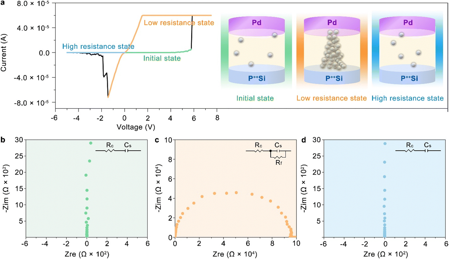 | ||
| Fig. 4 (a) A typical cycle of I–V characteristics from 5 nm SiO2-based memristors is shown in a linear–linear scale. The initial HRS, LRS (SET), and HRS (RESET) are colored with green, orange, and blue, sequentially. These three states are schematically explained on the right: the initial HRS of the device has a small number of intrinsic oxygen vacancies (white ball shapes). At LRS, an oxygen vacancy-based conductive filament is well established, connecting the TE and BE. At the HRS resulting from RESET, the conductive filament is dissolved, and fewer oxygen vacancies are present again. (b) A Nyquist plot from EIS measurements on initial HRS of SiO2-based memristors, of which the vertical line shape (parallel to the y-axis) indicates the pseudo-pure capacitive property. Based on the simulation, the equivalent circuit consists of a resistor in series with a capacitor, and it is displayed in the upper right corner. (c) A semicircle shape appears in the Nyquist plot at LRS. Another resistor is paralleled with a capacitor in the simulated equivalent circuit. (d) The Nyquist plot at HRS after RESET becomes a straight-line shape again. The associated equivalent circuit is back to a series connection of one resistor and one capacitor. | ||
As a two-terminal device, memristors, consisting of a switching layer and two electrodes in a simple sandwich structure closely resemble the structure of a chemical synapse in the brain. This similarity is demonstrated schematically in Fig. 5a, particularly in the orange dashed circle for the synapse and the blue dashed circle for the memristor. The synaptic cleft corresponds to the switching layer of the memristor, while the pre-synapse and the post-synapse correspond to the top electrode and the bottom electrode of the memristor, respectively.
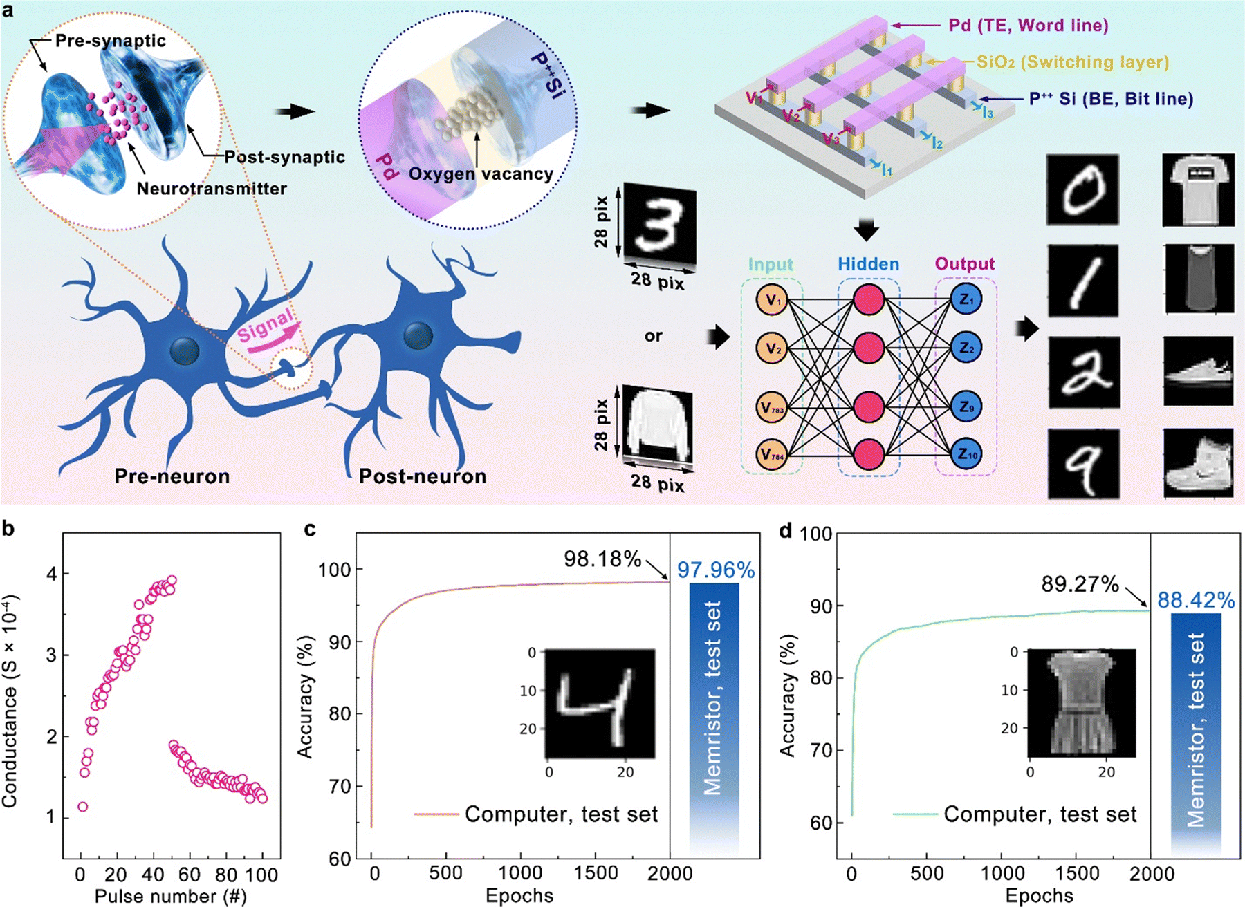 | ||
| Fig. 5 (a) The process for signal transportation between neurons. The structure and function of the synapse in this process are illustrated in the dashed orange circle (left). In the dashed blue circle (right), the synapse is schematically embedded into the SiO2-based memristor to demonstrate the similarity between them. Next, a SiO2-based memristive crossbar prototype is exhibited towards neuromorphic computing. Finally, a neural network for image recognition is explained with instances from MNIST and fashion MNIST data sets (b) the synaptic characteristics evaluated from SiO2-based memristors with 50 identical positive pulses and 50 identical negative pulses, demonstrating gradual variations of the conductance. The model accuracy examinations with (c) MNIST and (d) fashion MNIST as a function of epochs on test sets. | ||
In the signal transmission process from one neuron to the next, as illustrated in Fig. 5a, the action potential (i.e., pulse bias in memristor operation) is first transferred from the soma to the end of the neuron (i.e., the presynaptic neuron) via the axon.43 Then, from the presynaptic neuron, synaptic weights are altered by the release of neurotransmitters. This neurotransmission process leads to the dynamic modulation of synaptic connection intensity. Our SiO2-based memristor can mimic this synaptic behavior by tuning the conductance level with electrical pulses. The mechanism of updating weights for SiO2-based memristor is similar to a chemical synapse, in which the oxygen vacancies function like neurotransmitters, forming a conductive path in the switching layer (i.e., connecting the top and bottom electrodes) and changing the conductance level of the device.44 A proposed SiO2-based memristor crossbar prototype is illustrated in the upper right corner of Fig. 5. Such crossbar structure features two sets of wire electrodes, categorized as word lines (WLs) and bit lines (BLs). At each junction where these wires intersect, a resistive switching layer is present. Voltage pulses are fed through WLs then traverse through synaptic crossbar and converge at the BLs. The resulting output current is a function of both the initial input voltages and the conductance properties of the memristors in the crossbar, as described by Ohm's and Kirchhoff's laws.45 We should note that the practical large-scale crossbar may experience disturbances caused by parasitic effects like series resistance and sneak path complications. The current flowing through the metal wires can cause a notable reduction in voltage, particularly affecting the cell at the greatest distance within the array. This phenomenon ultimately leads to what is commonly termed the “IR drop” problem. This issue not only compromises the reliability of memory read operations but also reduces the accuracy of vector-matrix multiplication computations. Reducing the wire resistance or enhancing the intrinsic resistance of the memristor can effectively address this issue by employing advanced device architectures that promote increased integration and scaling through the reduction of line width/length, along with the utilization of more highly conducting metallization. Another parasitic issue sneak path refers to an unintended electrical pathway that allows current to flow through multiple memristors, rather than through the targeted cell for a particular operation.46 Such sneak path issue may trigger operational malfunctions and excessive energy consumption.47 To alleviate the sneak path issue, various strategies involve redesigning the basic units. For example, adding an access component to the single-memristor (1R) cell can create composite cells like one-transistor-one-memristor (1T1R) or one-switch-one-memristor (1S1R) to suppress the sneak current.48
Neuromorphic computing capability of our SiO2-based memristors was evaluated through pulse measurements with the pulse width of 5 ms and with continuous 50 positive pulses, followed by 50 negative pulses at the amplitude of 5 V for both positive and negative pulses. In Fig. 5b, a prominent multi-conductance behavior is observed in the memristor, which mimics the information transportation between synapses. 10 cycles (a total of 1000 pulses) of LTP and LTD behaviors are achieved from our SiO2-based memristor (Fig. S12, ESI†), demonstrating consistent repeatability with a relatively linear potentiation behavior and a less linear trend in depression. It should be noted that the resistance state is within the LRS regime during the pulse measurements (i.e., dynamic range) where the conduction filament experiences thickening (potentiation) and shrinkage (depression).49 To validate this proposed switching mechanism, the retention (Fig. S13a and b, ESI†) and EIS (Fig. S13c–e, ESI†) measurements were conducted at three different LRS states. The Nyquist plots in Fig. S13c–e (ESI†) have a similar shape with one semicircle at LRS to that in the main text Fig. 4c, revealing that the filaments exist at multi-states of the device. Thus, the EIS results with the one semicircle shape and increased conductance support our proposed switching mechanism where (1) the synaptic process operates in the dynamic regime (i.e., conduction filament already formed between the TE and BE) and (2) the thickness of the conduction filament increases during the potentiation process.
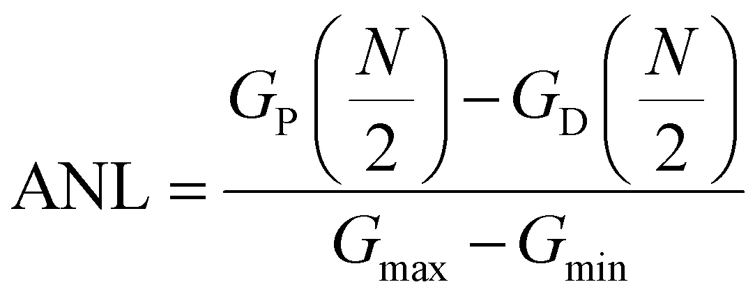
The asymmetric non-linearity factor (ANL) was calculated by using the following equation:
To demonstrate the neuromorphic computing performance of our memristor, we modeled a deep neural network (DNN) with 784 input neurons, 500 hidden neurons, and 10 output neurons based on our device. Further details on the simulation process are available in Note S2 (ESI†). The DNN is employed to perform image recognition tasks on the MNIST and fashion-MNIST datasets.54 The computing structure of the DNN is described in Fig. 5a with examples of datasets. The input images are initially converted into 28 × 28 matrices with values ranging from 0 to 255. These matrices are then flattened into vectors of length 784 and fed into the DNN. The 10 output neurons correspond to 10 distinct classes, with the neuron exhibiting the highest value representing the recognized result. The DNN is initially trained on conventional hardware for 2000 epochs, attaining accuracy levels of 98.2% and 89.3% for the MNIST and fashion-MNIST datasets, respectively. Subsequently, the trained weights are translated to conductance values based on our device's conductance changing curve. To facilitate this translation, a proportional mapping scheme is employed that maps continuous weights onto the closest discrete conductance states.53 Two memristors are utilized to implement positive and negative weights separately, with the maximum discrete weight set at 1 for positive memristors and −1 for negative memristors.53 Given the finite number of conduction states, the learning accuracy becomes 98.0% and 88.4% for MNIST and fashion-MNIST, respectively (Fig. 5c and d). The marginal reduction (0.2% and 0.9%) in recognition accuracy validates the promise of our memristor for future applications in neural networks and neuromorphic computing.
Conclusions
We demonstrated high performance SiO2-based memristors which can achieve a noteworthy on/off ratio as high as 1.4 × 10⁵ with long-term stability and endurance. The oxygen vacancy-driven switching mechanisms were complementarily identified through theoretical and experimental investigations. A multi-physical field coupled model based finite element simulations systematically revealed the evolution of the conduction filaments as a function of applied bias where the roughness of TE/SiO2 interface plays a significant role. The ∼1 nm protrusion causes variations in the local electric field and hence selectively forms a conduction filament, preferably at the higher electric field locations. EIS analyses complement the theoretical switching mechanism investigation by identifying equivalent circuit components of the memristor at initial, SET, and RESET processes. Associated Nyquist plots ascertain pseudo single capacitor behavior at the initial and RESET process, and a parallel structure of a capacitor and a resistor during the SET process. As a proof-of-concept, DNN was demonstrated with the parameters of our SiO2 memristors. The demonstrated SiO2-based memristors featuring a notable high on/off ratio and reasonable reliability as well as low thermal budget processing may be of direct relevance to next-generation computing devices that require energy-efficient and parallel processing.Methods
The SiO2 switching layer was deposited from a sintered ceramic SiO2 target in a magnetron sputtering system on heavily-doped Si wafers (<0.003–0.005 Ω cm). Before the sputtering process, the deposition chamber was pumped down to a base pressure of under 9 × 10⁻⁷ Torr. Pure Ar gas (15 sccm) was used as the sputter gas, leading to a working pressure of 1.7 × 10⁻³ Torr at an RF power of 150 W. Then, the deposited SiO2 layer was annealed at 550 °C for 10 hours. A layer of palladium (Pd) was deposited as the top electrode (TE) on the annealed SiO2/Si structure through a thermal evaporation system equipped with a 6 MHz oscillating quartz crystal sensor to monitor the growth rate and thickness. A shadow mask was utilized to define the shape and size of the TE during its fabrication. The thickness of the SiO2 layer (5, 10, 20, and 30 nm) was verified by a Multi-Wavelength Ellipsometer (FilmSense FS-1) using an incident and detection angle of 65°. An FEI Themis Z TEM microscope equipped with an energy dispersive spectroscopy (EDS) was employed to examine the structures and map elemental distribution in Pd/SiO2/P++Si memristors. The pattern of the top electrode was verified in plan-view images by an FEI Nova NanoSEM system.DC current–voltage (I–V) sweeping evaluations of all SiO2-based memristors were carried out using a semiconductor parameter analyzer (Agilent 4155B) connected to a probe station in a dark shield box. Capacitance–voltage (C–V) characteristics were performed with a precision LCR meter (Agilent 4284A). Electrochemical impedance spectroscopy (EIS) investigations were conducted in an electrochemical workstation (VersaSTAT3 Princeton) by using a frequency range of 1 MHz to 1 Hz. For the pulse measurement, the Agilent 33120A function arbitrary waveform generator provided the pulse profile, which could be conveniently designed by the Agilent IntuiLink Waveform Editor. A digital storage oscilloscope (Hantek DSO4254B) was utilized to monitor the pulse voltages, and the Agilent 4155B SMU was used to record the corresponding current. Physical Modeling details for finite element analysis can be found in Note S1 (ESI†) while detailed simulation for image processing is elaborated in Note S2 in the ESI.†
Author contributions
F. Q. and Y. Z.: conceptualization, characterization for memristors’ performance, finite element analysis, draft writing. Z. G.: image processing simulation. C. K., J. P., and K. N.: TEM characterization. X. F.: assistance with electrical measurements. T. P., H. P., H. S., X. R., and S. L.: conceptualization, methodology, supervision, funding acquisition, writing, review, and editing.Conflicts of interest
The authors declare no competing financial interest.Acknowledgements
This work was partially supported by National Science Foundation, Award number ECCS-1931088 and CBET-2207302. S. L. and H. W. S. acknowledge the support from the Improvement of Measurement Standards and Technology for Mechanical Metrology (Grant No. 23011043) by KRISS. The authors would like to thank Dr. Kejie Zhao for providing the electrochemical workstation.References
- (a) I. Valov, R. Waser, J. R. Jameson and M. N. Kozicki, Nanotechnology, 2011, 22, 254003 CrossRef PubMed; (b) S. Jung, H. Lee, S. Myung, H. Kim, S. K. Yoon, S.-W. Kwon, Y. Ju, M. Kim, W. Yi, S. Han, B. Kwon, B. Seo, K. Lee, G.-H. Koh, K. Lee, Y. Song, C. Choi, D. Ham and S. J. Kim, Nature, 2022, 601, 211 CrossRef CAS PubMed.
- (a) C. H. Kim, Y. H. Jang, H. J. Hwang, C. H. Song, Y. S. Yang and J. H. Cho, Appl. Phys. Lett., 2010, 97, 062109 CrossRef; (b) F. Qin, Y. Zhang, H. Park, C. S. Kim, D. H. Lee, Z.-T. Jiang, J. Park, K. No, H. Park, H. W. Song and S. Lee, Phys. Status Solidi RRL, 2022, 2200075 CrossRef CAS.
- (a) W. Li, X. Liu, Y. Wang, Z. Dai, W. Wu, L. Cheng, Y. Zhang, Q. Liu, X. Xiao and C. Jiang, Appl. Phys. Lett., 2016, 108, 153501 CrossRef; (b) A. Mehonic, T. Gerard and A. J. Kenyon, Appl. Phys. Lett., 2017, 111, 233502 CrossRef.
- (a) Y. H. Jang, W. Kim, J. Kim, K. S. Woo, H. J. Lee, J. W. Jeon, S. K. Shim, J. Han and C. S. Hwang, Nat. Commun., 2021, 12, 5727 CrossRef CAS PubMed; (b) L. Wu, H. Liu, J. Li, S. Wang and X. Wang, Nanoscale Res. Lett., 2019, 14, 177 CrossRef PubMed.
- (a) M. D. Pickett, D. B. Strukov, J. L. Borghetti, J. J. Yang, G. S. Snider, D. R. Stewart and R. S. Williams, J. Appl. Phys., 2009, 106, 074508 CrossRef; (b) T. S. Lee and C. Choi, Nanotechnology, 2022, 33, 245202 CrossRef CAS PubMed.
- (a) Y. Y. Illarionov, T. Knobloch, M. Jech, M. Lanza, D. Akinwande, M. I. Vexler, T. Mueller, M. C. Lemme, G. Fiori, F. Schwierz and T. Grasser, Nat. Commun., 2020, 11, 3385 CrossRef CAS PubMed; (b) K. P. Cheung, J. Appl. Phys., 2022, 132, 144505 CrossRef CAS PubMed.
- (a) A. Padovani, D. Z. Gao, A. L. Shluger and L. Larcher, J. Appl. Phys., 2017, 121, 155101 CrossRef; (b) S. Hideki and T. Akira, Semicond. Sci. Technol., 2000, 15, 471 CrossRef; (c) S. J. Moxim, F. V. Sharov, D. R. Hughart, G. S. Haase, C. G. McKay and P. M. Lenahan, Appl. Phys. Lett., 2022, 120, 063502 CrossRef CAS.
- (a) J. Yao, Z. Sun, L. Zhong, D. Natelson and J. M. Tour, Nano Lett., 2010, 10, 4105 CrossRef CAS PubMed; (b) A. Mehonic, S. Cueff, M. Wojdak, S. Hudziak, O. Jambois, C. Labbé, B. Garrido, R. Rizk and A. J. Kenyon, J. Appl. Phys., 2012, 111, 074507 CrossRef.
- A. Mehonic, A. L. Shluger, D. Gao, I. Valov, E. Miranda, D. Ielmini, A. Bricalli, E. Ambrosi, C. Li, J. J. Yang, Q. Xia and A. J. Kenyon, Adv. Mater., 2018, 30, 1801187 CrossRef PubMed.
- (a) C. Li, L. Han, H. Jiang, M.-H. Jang, P. Lin, Q. Wu, M. Barnell, J. J. Yang, H. L. Xin and Q. Xia, Nat. Commun., 2017, 8, 15666 CrossRef CAS PubMed; (b) A. Mehonic, M. S. Munde, W. H. Ng, M. Buckwell, L. Montesi, M. Bosman, A. L. Shluger and A. J. Kenyon, Microelectron. Eng., 2017, 178, 98 CrossRef CAS; (c) N. Ilyas, C. Li, J. Wang, X. Jiang, H. Fu, F. Liu, D. Gu, Y. Jiang and W. Li, J. Phys. Chem. Lett., 2022, 13, 884 CrossRef CAS PubMed; (d) C. Li, H. Jiang and Q. Xia, Appl. Phys. Lett., 2013, 103, 062104 CrossRef; (e) A. Mehonic, S. Cueff, M. Wojdak, S. Hudziak, C. Labbé, R. Rizk and A. J. Kenyon, Nanotechnology, 2012, 23, 455201 CrossRef PubMed.
- N. Ilyas, J. Wang, C. Li, H. Fu, D. Li, X. Jiang, D. Gu, Y. Jiang and W. Li, J. Mater. Sci. Technol., 2022, 97, 254 CrossRef CAS.
- S. Choi, G. S. Kim, J. Yang, H. Cho, C.-Y. Kang and G. Wang, Adv. Mater., 2022, 34, 2104598 CrossRef CAS PubMed.
- Y. Huang, Z. Shen, Y. Wu, X. Wang, S. Zhang, X. Shi and H. Zeng, RSC Adv., 2016, 6, 17867 RSC.
- J. Zhu, T. Zhang, Y. Yang and R. Huang, Appl. Phys. Rev., 2020, 7, 011312 CAS.
- (a) Y. Yang, P. Gao, S. Gaba, T. Chang, X. Pan and W. Lu, Nat. Commun., 2012, 3, 732 CrossRef PubMed; (b) J. H. Yoon, J. Zhang, P. Lin, N. Upadhyay, P. Yan, Y. Liu, Q. Xia and J. J. Yang, Adv. Mater., 2020, 32, 1904599 CrossRef CAS PubMed.
- (a) M. Buckwell, L. Montesi, S. Hudziak, A. Mehonic and A. J. Kenyon, Nanoscale, 2015, 7, 18030 RSC; (b) U. Celano, L. Goux, A. Belmonte, K. Opsomer, A. Franquet, A. Schulze, C. Detavernier, O. Richard, H. Bender, M. Jurczak and W. Vandervorst, Nano Lett., 2014, 14, 2401 CrossRef CAS PubMed.
- (a) G. Di Martino, A. Demetriadou, W. Li, D. Kos, B. Zhu, X. Wang, B. de Nijs, H. Wang, J. MacManus-Driscoll and J. J. Baumberg, Nat. Electron., 2020, 3, 687 CrossRef CAS; (b) J. Y. Chen, C. W. Huang, C. H. Chiu, Y. T. Huang and W. W. Wu, Adv. Mater., 2015, 27, 5028 CrossRef CAS PubMed.
- B. El-Kareh, Fundamentals of semiconductor processing technologies, Kluwer Academic Publishers, Boston, Massachusetts, 1995 Search PubMed.
- Y. Zhang, Z. Wang, J. Zhu, Y. Yang, M. Rao, W. Song, Y. Zhuo, X. Zhang, M. Cui, L. Shen, R. Huang and J. Joshua Yang, Appl. Phys. Rev., 2020, 7, 011308 CAS.
- F. M. Simanjuntak, D. Panda, K. H. Wei and T. Y. Tseng, Nanoscale Res. Lett., 2016, 11 Search PubMed.
- (a) S. Kumar, M. Das, M. T. Htay, S. Sriram and S. Mukherjee, ACS Appl. Electron. Mater., 2022, 4, 3080 CrossRef CAS; (b) G. S. Kim, H. Song, Y. K. Lee, J. H. Kim, W. Kim, T. H. Park, H. J. Kim, K. Min Kim and C. S. Hwang, ACS Appl. Mater. Interfaces, 2019, 11, 47063 CrossRef CAS PubMed.
- (a) M. Song, S. Lee, S. S. T. Nibhanupudi, J. V. Singh, M. Disiena, C. J. Luth, S. Wu, M. J. Coupin, J. H. Warner and S. K. Banerjee, Nano Lett., 2023, 23, 2952 CrossRef CAS PubMed; (b) T. S. Lee, N. J. Lee, H. Abbas, H. H. Lee, T. S. Yoon and C. J. Kang, ACS Appl. Electron. Mater., 2020, 2, 1154 CrossRef CAS.
- (a) Z. Liu, P. Cheng, R. Kang, J. Zhou, X. Zhao, J. Zhao and Z. Zuo, Adv. Mater. Interfaces, 2023, 10, 2201513 CrossRef CAS; (b) Y. Sun, X. Yan, X. Zheng, Y. Liu, Y. Zhao, Y. Shen, Q. Liao and Y. Zhang, ACS Appl. Mater. Interfaces, 2015, 7, 7382 CrossRef CAS PubMed.
- W. Wang, F. Yin, H. Niu, Y. Li, E. S. Kim and N. Y. Kim, Nano Energy, 2023, 106, 108072 CrossRef CAS.
- J.-H. Ryu, F. Hussain, C. Mahata, M. Ismail, Y. Abbas, M.-H. Kim, C. Choi, B.-G. Park and S. Kim, Appl. Surf. Sci., 2020, 529, 147167 CrossRef CAS.
- O. K. Prasad, S. Chandrasekaran, C.-H. Chung, K.-M. Chang and F. M. Simanjuntak, Appl. Phys. Lett., 2022, 121, 233505 CrossRef CAS.
- S. Roy, G. Niu, Q. Wang, Y. Wang, Y. Zhang, H. Wu, S. Zhai, P. Shi, S. Song, Z. Song, Z. G. Ye, C. Wenger, T. Schroeder, Y. H. Xie, X. Meng, W. Luo and W. Ren, ACS Appl. Mater. Interfaces, 2020, 12, 10648 CrossRef CAS PubMed.
- M. Ismail, C. Mahata and S. Kim, J. Alloys Compd., 2022, 892, 162141 CrossRef CAS.
- I. Zrinski, C. C. Mardare, L.-I. Jinga, J. P. Kollender, G. Socol, A. W. Hassel and A. I. Mardare, Appl. Surf. Sci., 2021, 548, 149093 CrossRef CAS.
- F. Xiong, Z. Wang, E. D. Bøjesen, X. Xiong, Z. Zhu and M. Dong, Small, 2021, 17, 1 Search PubMed.
- Y. F. Chang, L. Ji, Y. Wang, P. Y. Chen, F. Zhou, F. Xue, B. Fowler, E. T. Yu and J. C. Lee, Appl. Phys. Lett., 2013, 103, 193508 CrossRef.
- Chemical elements by market price, http://www.leonland.de/elements_by_price/en/list, (accessed December 2023).
- H. Dou, X. Gao, D. Zhang, S. Dhole, Z. Qi, B. Yang, M. N. Hasan, J.-H. Seo, Q. Jia, M. Hellenbrand, J. L. MacManus-Driscoll, X. Zhang and H. Wang, ACS Appl. Electron. Mater., 2021, 3, 5278 CrossRef CAS.
- (a) M. Kim, M. A. Rehman, D. Lee, Y. Wang, D.-H. Lim, M. F. Khan, H. Choi, Q. Y. Shao, J. Suh, H.-S. Lee and H.-H. Park, ACS Appl. Mater. Interfaces, 2022, 14, 44561 CrossRef CAS PubMed; (b) M.-C. Chen, T.-C. Chang, S.-Y. Huang, S.-C. Chen, C.-W. Hu, C.-T. Tsai and S. M. Sze, Electrochem. Solid-State Lett., 2010, 13, H191 CrossRef CAS.
- (a) N. Ghenzi, M. J. Rozenberg, R. Llopis, P. Levy, L. E. Hueso and P. Stoliar, Appl. Phys. Lett., 2015, 106 Search PubMed; (b) Z. Q. Wang, H. Y. Xu, X. H. Li, X. T. Zhang, Y. X. Liu and Y. C. Liu, IEEE Electron Device Lett., 2011, 32, 1442 CAS.
- D. Lin, Y. Liu and Y. Cui, Nat. Nanotechnol., 2017, 12, 194 CrossRef CAS PubMed.
- J.-Y. Chen, C.-L. Hsin, C.-W. Huang, C.-H. Chiu, Y.-T. Huang, S.-J. Lin, W.-W. Wu and L.-J. Chen, Nano Lett., 2013, 13, 3671 CrossRef CAS PubMed.
- T. Wei, Y. Lu, F. Zhang, J. Tang, B. Gao, P. Yu, H. Qian and H. Wu, Adv. Mater., 2023, 35, 2209925 CrossRef CAS PubMed.
- (a) D.-H. Kwon, K. M. Kim, J. H. Jang, J. M. Jeon, M. H. Lee, G. H. Kim, X.-S. Li, G.-S. Park, B. Lee, S. Han, M. Kim and C. S. Hwang, Nat. Nanotechnol., 2010, 5, 148 CrossRef CAS PubMed; (b) A. Mehonic, M. Buckwell, L. Montesi, M. S. Munde, D. Gao, S. Hudziak, R. J. Chater, S. Fearn, D. McPhail, M. Bosman, A. L. Shluger and A. J. Kenyon, Adv. Mater., 2016, 28, 7486 CrossRef CAS PubMed.
- (a) Y. Zhang, C. S. Kim, H. W. Song, S.-J. Chang, H. Kim, J. Park, S. Hu, K. Zhao and S. Lee, Energy Storage Mater., 2022, 48, 1 CrossRef; (b) C. S. Dash, S. Sahoo and S. R. S. Prabaharan, Solid State Ionics, 2018, 324, 218 CrossRef CAS.
- F. Qin, Y. Zhang, H. W. Song and S. Lee, Mater. Adv., 2023, 4, 1850 RSC.
- Y. Li, Y. P. Zhong, J. J. Zhang, X. H. Xu, Q. Wang, L. Xu, H. J. Sun and X. S. Miao, Appl. Phys. Lett., 2013, 103, 043501 CrossRef.
- W. Yi, K. K. Tsang, S. K. Lam, X. Bai, J. A. Crowell and E. A. Flores, Nat. Commun., 2018, 9, 4661 CrossRef PubMed.
- (a) W. Huang, X. Xia, C. Zhu, P. Steichen, W. Quan, W. Mao, J. Yang, L. Chu and X. A. Li, Nano-Micro Lett., 2021, 13, 85 CrossRef CAS PubMed; (b) R. Waser, R. Dittmann, G. Staikov and K. Szot, Adv. Mater., 2009, 21, 2632 CrossRef CAS PubMed.
- Q. Xia and J. J. Yang, Nat. Mater., 2019, 18, 309 CrossRef CAS PubMed.
- (a) M. A. Zidan, H. A. H. Fahmy, M. M. Hussain and K. N. Salama, Microelectron. J., 2013, 44, 176 CrossRef; (b) Y. Cassuto, S. Kvatinsky and E. Yaakobi, presented at 2013 IEEE International Symposium on Information Theory, 7–12 July 2013, 2013.
- Y. Li and K.-W. Ang, Adv. Intelligent Systems, 2021, 3, 2000137 CrossRef.
- H. Li, S. Wang, X. Zhang, W. Wang, R. Yang, Z. Sun, W. Feng, P. Lin, Z. Wang, L. Sun and Y. Yao, Adv. Intelligent Systems, 2021, 3, 2100017 CrossRef.
- S.-O. Park, T. Park, H. Jeong, S. Hong, S. Seo, Y. Kwon, J. Lee and S. Choi, Nanoscale Horiz., 2023, 8, 1366 RSC.
- H. Yeon, P. Lin, C. Choi, S. H. Tan, Y. Park, D. Lee, J. Lee, F. Xu, B. Gao, H. Wu, H. Qian, Y. Nie, S. Kim and J. Kim, Nat. Nanotechnol., 2020, 15, 574 CrossRef CAS PubMed.
- A. Shaban, S. S. Bezugam and M. Suri, Nat. Commun., 2021, 12, 4234 CrossRef CAS PubMed.
- (a) J. Park, E. Park, S.-G. Kim, D.-G. Jin and H.-Y. Yu, ACS Appl. Electron. Mater., 2021, 3, 5584 CrossRef CAS; (b) D. S. Kim, H. W. Suh, S. W. Cho, S. Y. Oh, H. H. Lee, K. W. Lee, J. H. Choi and H. K. Cho, Mater. Horiz., 2023, 10, 3382 RSC; (c) C. C. Chang, P. C. Chen, T. Chou, I. T. Wang, B. Hudec, C. C. Chang, C. M. Tsai, T. S. Chang and T. H. Hou, IEEE J. Emerging Selected Top. Circuits Systems, 2018, 8, 116 Search PubMed; (d) A. Krishnaprasad, D. Dev, S. S. Han, Y. Shen, H.-S. Chung, T.-S. Bae, C. Yoo, Y. Jung, M. Lanza and T. Roy, ACS Nano, 2022, 16, 2866 CrossRef CAS PubMed.
- A. Mehonic, D. Joksas, W. H. Ng, M. Buckwell and A. J. Kenyon, Front. Neurosci., 2019, 13 DOI:10.3389/fnins.2019.00593.
- (a) Y. Lecun, L. Bottou, Y. Bengio and P. Haffner, Proc. IEEE, 1998, 86, 2278 CrossRef; (b) H. Xiao, K. Rasul and R. Vollgraf, arXiv, 2017, preprint arXiv:1708.07747.
Footnotes |
| † Electronic supplementary information (ESI) available: CV measurements on devices with different thickness of SiO2, retention characteristics on 5 nm SiO2 memristor, the electric field distribution within 5 nm SiO2 switching layer at different stages, I–V DC sweeping characteristics of different thicknesses of SiO2 switching layer, the oxygen vacancy evolution and the electric field distribution of memristor with 10 nm SiO2 switching layer at different stages, gradual switching behavior of the 5 nm SiO2 memristor, physical modeling detail, and image processing detail. See DOI: https://doi.org/10.1039/d3ma01142a |
| ‡ F. Q. and Y. Z. contributed equally to this work. |
| This journal is © The Royal Society of Chemistry 2024 |