DOI:
10.1039/D3MA01127E
(Paper)
Mater. Adv., 2024,
5, 3220-3227
Detrapping of the carriers from shallow states in a highly responsive, fast, broadband (UV-vis-NIR), self-powered SnSe/Si photodetector with asymmetric metal electrodes†
Received
15th December 2023
, Accepted 16th February 2024
First published on 16th February 2024
Abstract
Tin-selenide (SnSe), as an eco-friendly and low-cost semiconductor material, has exhibited great potential to detect weak signals and has wide applications in imaging and optical communication. Here, self-powered SnSe-based photodetectors (PDs) via asymmetric metal electrodes are fabricated to achieve weak light detection for broad spectral ranges from 385 to 1064 nm with high response and fast response (on/off) times. The results show that the SnSe PDs are highly sensitive in a wide spectral range from UV to NIR, even at 0 V applied bias. They exhibit an excellent responsivity (R) of 54.7 mA W−1 and detectivity (D) of 7.87 × 10¹⁰ Jones, corresponding to rise/decay times of 26/47 ms under 1064 nm illumination at 0 V applied bias, respectively. With increasing the bias, detrapping of the carriers can be seen from the shallow trap states arising from the secondary phases in the SnSe. The results suggest that SnSe-based PDs obtained from the evaporation method have great potential in developing low-cost, next-generation, and self-powered optoelectronics.
1. Introduction
Over the past few decades, broad spectral photodetectors (PDs) have been extensively utilized in diverse fields, including optical communications, image processing, bioimaging, process control, chemical analysis, astronomy, security, thermal imaging, defense, night vision, environmental monitoring, process control, etc.1–5 Several inorganic semiconductor thin film materials, i.e., perovskite,6 2D-materials,7 graphene,8 CuInGaSe2,9 Cu2ZnSnS4,10 Sb2Se3,11 GaN,12 PbS,13etc., have been explored regarding their capability for broadband photodetection. The above materials can absorb specific electromagnetic spectra and generate appropriate signals for various applications. Recently, self-powered broadband thin-film PDs have received enormous recognition and hold great promise due to their built-in photoelectric detection capability, excellent responsivity (R), broadband photodetection, high detectivity (D), ultrafast speed (on/off), and high external quantum efficiency (EQE) even at 0 V applied bias.14–16 Thin-film PDs with self-powered characteristics can open a new avenue for next-generation flexible optoelectronics.
Graphene,17 perovskite,18 and MoS219 materials have displayed excellent performance; however, their large-scale commercial production is hindered due to their low absorption, stability issues, and complex fabrication processes. Furthermore, CuInGaSe2 has also been explored for broadband photodetection from visible to near-infrared (Vis-NIR), but the presence of rare and expensive elements, i.e., In and Ga, restricts their practical applications.20 Moreover, Cu2ZnSn(S,Se)4 has attractive optoelectronic properties like low-cost, eco-friendly nature, formation from earth-abundant elements, but suffers from low minority-carrier lifetime and intrinsic defect formation, resulting in low device performance compared to similar materials.21,22 These issues suggest the search for an alternative material with a less complex fabrication process, low-cost, earth-abundance, eco-friendly nature, and optoelectronic properties similar to CuInGaSe2 and other materials. In recent times, binary element-based semiconductor materials such as SnSe thin films have gained enormous attention owing to their suitable thermoelectric23–25 and optoelectronic properties,26–29i.e., low-cost, eco-friendliness, earth-abundance, tunable bandgap (from 1.1 to 1.7 eV), high optical absorption coefficient (∼105 cm−1), and chemical stability.30 Yan et al.31 developed flexible, ultra-broadband SnSe PDs that exhibited a spectral response up to 10.6 μm enabled by the photo-bolometric effect. Dong et al.32 reported 2D layered SnSe films for a UV-visible-NIR PD array with a high R of 277.3 A W−1, EQE of 8.5 × 10⁴%, and D of 7.6 × 10¹¹ Jones. Moreover, Jianfeng et al.33 fabricated broadband, self-powered SnSe PDs via an ultrafast laser. Despite excellent PD device performance, complex and expensive fabrication processes hinder their practical applications. Meanwhile, SnSe thin films grown using thermal evaporation offer a less complicated fabrication process, suggesting a potential route to develop SnSe-based high-quality absorber materials for optoelectronic devices.
Herein, we report self-powered, broadband SnSe-based PDs fabricated on a n-Si substrate using thermal evaporation. This study observed the effect of asymmetric metal electrodes on the SnSe PD performance. The fabricated SnSe device exhibits excellent broadband (Vis-NIR) photoresponse at 0 V applied bias voltage with an R of 54.7 mA W−1 and D of 7.87 × 10¹⁰ Jones under 1064 nm. Moreover, fast rise/decay (on/off) times of 26/47 ms under 1064 nm at 0 V applied bias were observed. The existence of the shallow states acts as a trapping center for the carriers at low biases. In contrast, the higher bias triggers the detrapping of the carriers, as inferred from the power law and ultrafast pump–probe study. This study suggests insights for developing low-cost and self-powered SnSe-based next-generation optoelectronic devices.
2. Experimental details
SnSe thin films were deposited onto the n-Si substrate from in-house-grown SnSe powder (synthesized using the solid-state reaction method) via thermal evaporation. Detailed synthesis and deposition conditions of the SnSe thin films can be found in our previous reports.34,35 The oxide layer formed on the n-Si substrate was not removed intentionally, so there was a SiO2 layer on the n-Si substrate. The amorphous nature of the SiO2 helps to achieve the neutral and smooth surficial characteristics that help to reduce the lattice mismatch.36 The asymmetric Pt and Ag metal contact on the SnSe/n-Si thin film was deposited using sputtering and thermal evaporation methods via shadow masking with a spacing between the two electrodes of about 100 microns. The performance of the fabricated SnSe PDs was measured using different laser light illuminations (i.e., 385, 532, and 1064 nm) via a photodetection measurement facility (Cascade Microtech EPS150TRIAX), kept in a shielded enclosure (EPS-ACC-SE750) for low-signal measurements.
3. Results and discussion
3.1. Structural, optical, and morphological properties
The structural properties of the SnSe thin film were characterized using X-ray diffraction (XRD) and Raman spectroscopy. Fig. 1(a) shows that the XRD spectra of the SnSe thin film match well with the JCPDS data 89-0232 and reveal the presence of the pure SnSe phase. The peak at 14.18° showed the presence of the SnSe2 phase (depicted as (001)SnSe2 red highlighted in Fig. 1(a)).35 Raman spectroscopy was carried out to confirm the SnSe phase further and peaks were observed at 70.67, 102.9, 128.16, and 153.24 cm−1 corresponding to the SnSe phase of the Ag1, B3g, Ag2, and Ag3 modes, respectively (Fig. 1(b)).34 The Raman spectra show small peaks at 182.20 and 217.89 cm−1 corresponding to the SnSe2 (A1g mode) and rutile SnO2,37 respectively, whereas the peak at 521.16 cm−1 is assigned to the Si substrate.36 From the Raman spectra, it is evident that the SnSe thin film is oxidized to a small extent. Oxidation of the SnSe thin film led to the presence of SnO2 and, after rearrangement, the SnSe2 phase.38,39Fig. 1(c) shows the Tauc plot of SnSe thin film estimated using ultra-visible spectroscopy and an estimated bandgap of about 1.36 eV, and there is some absorption around 1.0 eV. Fig. 1(d) shows the scanning electron microscope (SEM) image of the SnSe thin film deposited using thermal evaporation on the Si substrate. The SEM image shows the formation of petal-type nanostructures of SnSe thin film prepared using the thermal evaporation method. Matthew et al.40 demonstrated nanosheets of SnSe deposited onto a soda-lime glass (SLG) substrate using thermal evaporation. They observed nanosheets formed throughout the film, and these uniformly distributed nanosheets may develop because of an initial energetic preferential interaction with the glass substrate, which is maintained throughout the growth of the SnSe film. Singh et al.41 reported petal-type nanostructured Cu2ZnSnS4 (CZTS) thin films and studied their optical, structural, and morphological properties. Gour et al.10 demonstrated rice-like nanostructures of CZTS thin films on an SLG substrate deposited using sputtering and exhibited improved broadband (Vis-NIR) self-powered photodetection. They observed an enhanced optical absorption coefficient (105 cm−1) owing to the surface modification of CZTS thin film.
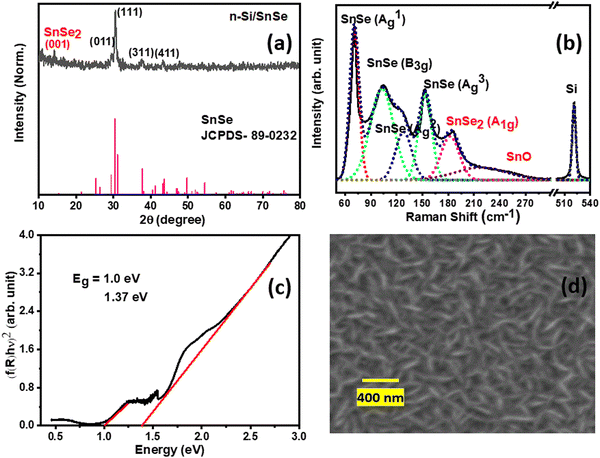 |
| | Fig. 1 (a) XRD spectra, (b) Raman analysis, (c) Tauc plot, and (d) SEM image of the SnSe/n-Si thin film. | |
3.2. Optoelectronic properties under different laser light illumination conditions
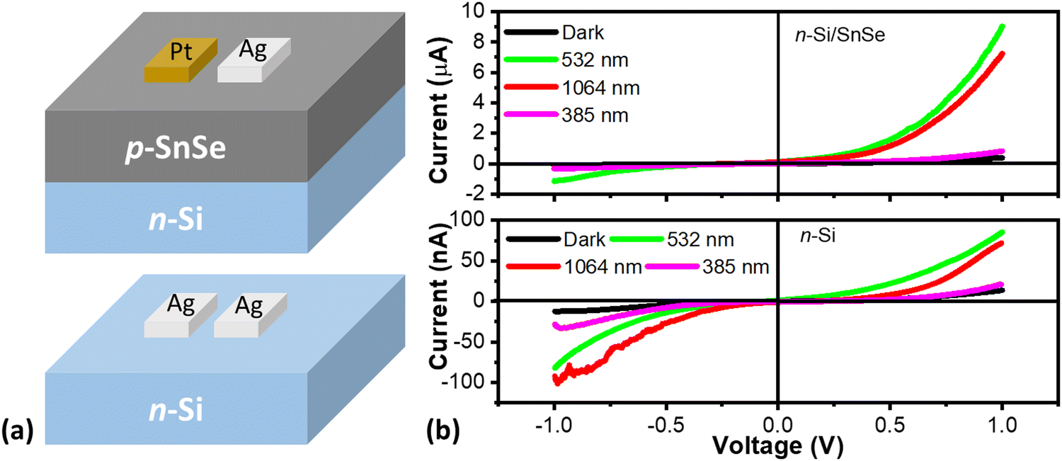
Fig. 2(a) shows the device architecture and Fig. 2(b) the current–voltage (I–V) measurement characteristics of the devices SnSe/n-Si and bare n-Si in the dark and under different laser light illuminations (385, 532, and 1064 nm). The device is shown in Fig. S1(a) (ESI†). SnSe on the n-Si substrate shows Schottky behavior with the electrodes, resulting in self-powered characteristics.32 The work function of a semiconductor depends on the material's thickness, strain, and stress.42,43 The substrate choice induces different strain/stress on the deposited thin film, which may lead to the Schottky behavior of the Ag electrode on SnSe thin films. The Ag electrodes on the n-Si show Schottky behavior as the work function of Ag is greater than the work function of the n-Si semiconductor.44 The bare n-Si-based device (Fig. S1(b), ESI†) performance was measured under different wavelengths at 250 mV applied bias under different laser light illuminations of 385, 532, and 1064 nm (Fig. S1(c)–(e), ESI†). The performance of the PDs has been estimated based on figures-of-merit, i.e., photocurrent (Iph), R, D, noise equivalent power (NEP), and response time (on/off) using the following eqn (1) and (2), where P is the optical power density of the incident photons illuminated, A is the active area of the device, Iph is photocurrent and Id is dark current, respectively.45,46| |  | (2) |
| |  | (3) |
| |  | (4) |
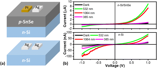 |
| | Fig. 2 (a) Schematic diagram of the devices and (b) device current–voltage (I–V) characteristics. | |
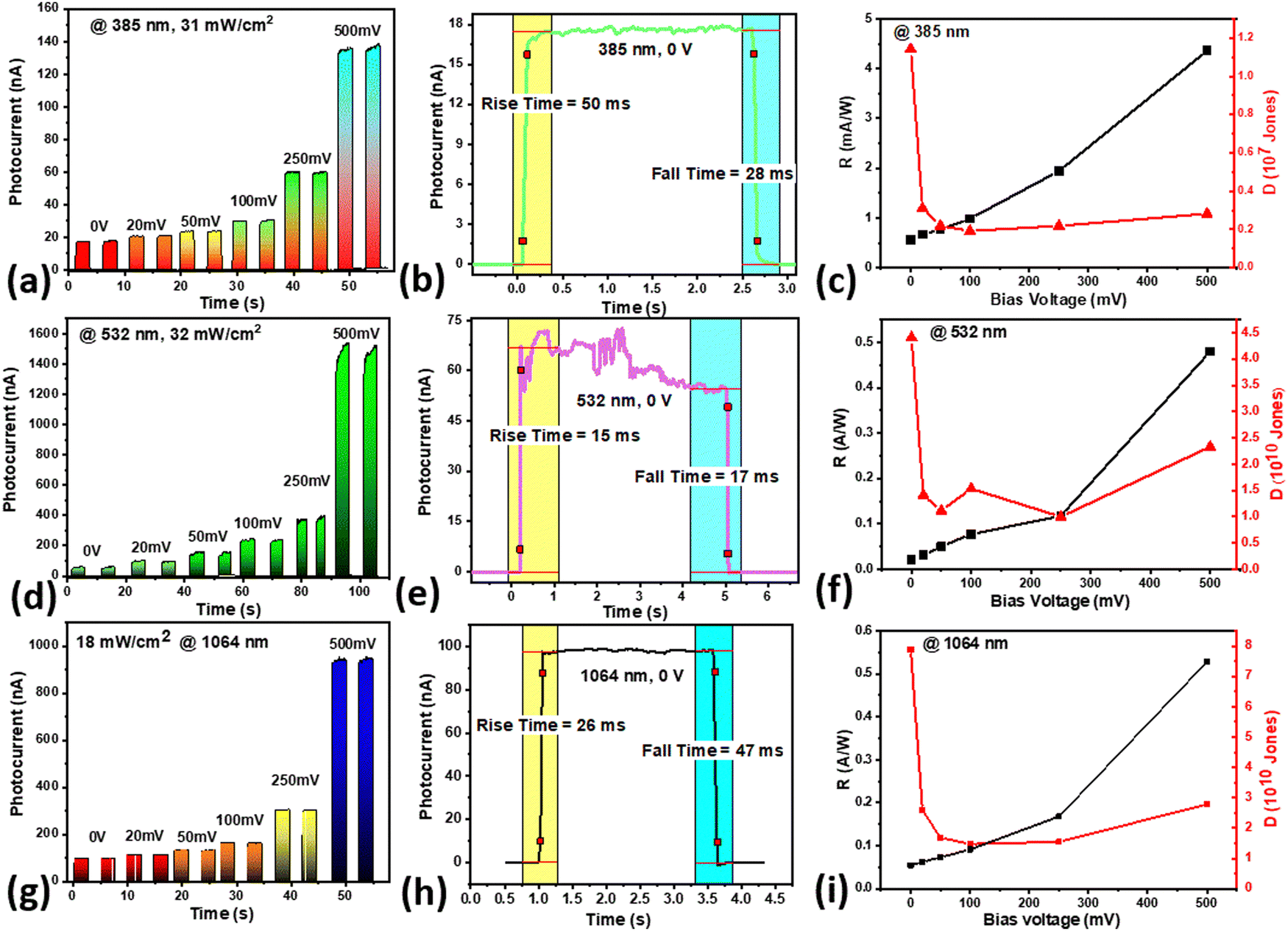
Fig. 3 shows the figure of merit of the SnSe PDs under different laser light illuminations, i.e., 385, 532, and 1064 nm at 0 V applied bias. The SnSe device performs under 385 nm mainly due to SnO, SiO2, and Si showing a photoresponse even in the UV region.32 In contrast, the photoresponse under 532 and 1064 nm laser illumination is contributed primarily by the SnSe thin film. The photocurrent of the device increases with the applied bias due to the increased drift velocity of the excited carriers. The device also showed performance under 0 V applied bias due to the asymmetric electrode contacts. Asymmetric contacts led to the different barrier heights at the electrodes and, hence, the net in-built electric field that directs the currents under zero bias (0 V) conditions.47 Many pieces of literature use this strategy due to its easy fabrication techniques.48–52 The photocurrent under 385 nm is less than that under 1064 nm and highest under 532 nm laser light illumination. The device showed a fast rise/decay (on/off) time of 50/28, 15/17, and 26/47 ms under 385, 532, and 1064 nm laser illumination at 0 V applied bias (Fig. 3). This swift response of the SnSe device has been linked to generating a high density of photons, potentially resulting in faster response times. Furthermore, the higher applied bias voltage attributed to increased drift velocity (Ttr = l2/[μ × Vb], where l is the length of the device, μ is the carrier mobility, and Vb is the applied bias voltage) and decreased carrier transit time of charge carriers results to swift rise/decay response times.46 The continuous cycling stability characteristics of the Sn-Se device under 385, 532, and 1064 nm laser light illumination under self-bias mode (0 V) are shown in Fig. 4(a)–(c). The photocurrent under a 532 nm laser shows an unstable value after the incident light due to the laser's unstable nature. The R and D under 385, 532, and 1064 nm laser light illumination at 0 V are shown in Fig. 4(d). Dynamic response curves of the dark current and NEP are shown in Fig. S2(a)–(c) (ESI†).
 |
| | Fig. 3 Cycles of photocurrent at different bias voltages, rise and decay times, and R and D at 0 V applied bias under different laser illuminations (385, 532, and 1064 nm) for SnSe/n-Si thin films. | |
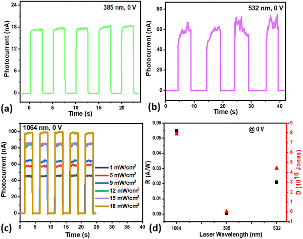 |
| | Fig. 4 Cyclic stability of the photoresponse of the device under (a) 385 nm, (b) 532 nm, (c) 1064 nm at different power densities, and (d) responsivity and detectivity of device at different lasers at zero bias. | |
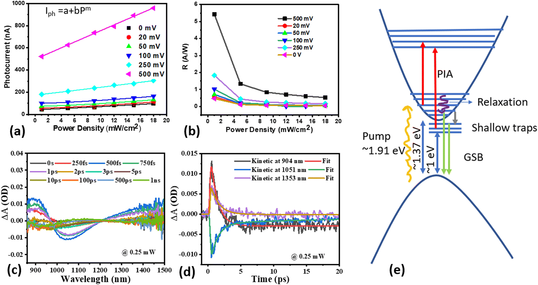
The estimated value of R and D is at its maximum under 1064 nm laser illumination. The continuous cycles of photocurrent at different power densities under a 1064 nm laser are shown in Fig. S2(d) (ESI†) at 500 mV bias and fitted with the power law for different voltages (Fig. 5(a)). The values of the exponents are 1.18, 1.22, 1.22, 1.08, 1.03, and 0.99 for the 0, 20, 50, 100, 250 and 500 mV biases, respectively. The value of the exponent tells a brief story of the photocurrent. The exponent value of 1.0 tells about the efficient separation of the carriers.53 A brief study of the power law and the value of the exponent's variation with bias is discussed in a previous report.54 After generating the carrier, their transport towards the channel and collection at appropriate electrodes give information about the scattering, defect, and trapping of the carrier. This information can be extracted from the value of the exponent. Here, the value of the exponent remains nearly the same with the bias (i.e., from 1.18 to 1.21 for 0 to 50 mV) and then gradually decreases from 1.21 to 0.99 with increasing bias potential from 50 to 500 mV.
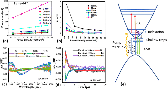 |
| | Fig. 5 (a) Power law fitting of the photocurrent at different voltages, and (b) R at different applied bias voltages under a 1064 nm laser, respectively. (c) Transient spectra and (d) kinetics at 0.25 mW fluence, and (e) schematic diagram of the possible trap states in the SnSe thin film. | |
Nearly the same value of the exponent from 0 to 50 mV indicates carriers' increasing average drift velocity within the transit length and, hence, the domination of the trap centres in the transport mechanism. These trapping states may arise due to the formation of secondary phase SnSe2. Also, the decreasing value of the exponent can be inferred like this. After increasing a specific voltage, there starts de-trapping of the carriers. The exponent value reaches the ideal value (here 0.99 at 500 mV), indicating the de-trapping of the carriers at 500 mV, and this process is triggered from 100 mV bias. Trapping should be from shallow states that fade away with increasing bias. Hence, the value of voltage-dependent power law indicates the domination of the trap/defect states in the device. It is noticeable that SnSe on the glass substrate showed non-dominant behavior of trap/defect states in the device. There was a regular pattern and increased exponent value in the voltage-dependent power law.34
This difference may arise due to several reasons, such as substrate nature (stress or strain in the device by substrate), time of exposure of the device in the atmosphere, the thickness of the film, etc.55Fig. 5(b) shows the relation between power density and R. Here, R decreases with increasing power density, which signifies the existence of trap or defect states responsible for this variation.56 If trapping states exist in the device, these should be limited. Their trapping effect can be prominent at lower power density due to less concentration of excited carriers. There are relatively more excited carriers at high power density whose trapping behavior is non-prominent. Hence, this trapping decreases the recombination of excited carriers. Therefore, the reduced behavior of the R with power density can be attributed to the trap or defect states in or at the device's interface.56 These trap/defect states may arise due to the slight oxidation of the substrate surface under working conditions of SnSe.39 To verify the existence of the shallow trapping states, ultrafast dynamics of the carriers were carried out. Transient spectra and kinetics at 0.25 mW fluence are shown in Fig. 5(c) and (d). There are three peaks: two positive and one negative. These positive and negative peaks are assigned to the photo-induced absorption and ground-state bleaching, respectively. The first positive peak corresponds to the absorption from either from conduction band or shallow trap states, and the peak beyond 1200 nm is due to absorption from the shallow trap states. Kinetics fitted at different wavelengths show the different relaxation mechanisms, recombination, and trapping. To confirm the existence of trap states, a pump fluence study was conducted at 0.50 and 1.0 mW. Transient spectra at a pump fluence of 0.25, 0.50, and 1.0 mW and their respective kinetic spectra are shown in Fig. S3 (ESI†). A detailed interpretation of the transient ultrafast data can be seen in the ESI.† A comparative transient spectrum at 500 fs probe delay is shown in Fig. S4 (ESI†). The kinetics at different wavelengths and their fitting at different pump fluences can be seen in Table S1 (ESI†).
In conclusion, the device has shallow traps, prominently due to the secondary phase (SnSe2), confirmed by both XRD and Raman spectroscopy. Fig. 5(e) shows a schematic diagram that concludes the ultrafast study and shallow traps in SnSe thin film. Also, the existence of a shallow trap can be verified by the fact that with increasing bias voltage (from 0–50 mV), the decay time of the device is nearly the same (i.e., ∼47–42 ms) under 1064 nm, while a further increase in applied bias results in a significant decrease in decay time (from 42 to 23 ms), as shown in Fig. S5 (ESI†). Moreover, the absorption contribution of around 1.0 eV might be due to these shallow trap states (Fig. 1(c)). The recovery process of the photocurrent should also show the trapping of the defect history of the carriers.47 Here, the decay nature of the photocurrent does not show the significant exponential tail that might be followed by shallow trapping of carriers. Furthermore, it is interesting to note the role of the n-Si substrate; the band alignment diagram is shown in Fig. S6(a) and (b) (ESI†) before and after the deposition. An in-built electric field is formed due to the difference in the work function values of the material. The flow direction of the current is from p-SnSe to n-Si due to the higher value of the Fermi level energies. Thus, this spontaneous flow of electrons helps achieve the p-type nature of the SnSe; therefore, it enhances the photocurrent. Table 1 compares the device performance of SnSe-based PDs at 0 V bias.
Table 1 Comparison of the device performance of SnSe-based PDs at 0 V applied bias
| Device architecture |
Substrate |
Laser source (nm) |
P (mW cm−2) |
τ
r (ms) |
τ
d (ms) |
D (Jones) |
R (mA W−1) |
Ref. |
| In/Si/SnSe/Pd vertical structure |
Si |
850 |
160 |
1.6 × 10⁻³ |
47.7 × 10⁻³ |
3.4 × 10¹² |
442.8 |
36
|
| Cr/Au/GeSe/Cr/Pd |
Si/SiO2 |
850 |
30 |
69 |
92 |
∼9.5 × 10¹⁰ |
∼430 |
48
|
| SnSe/InSe |
Si/SiO2 |
808 |
100 |
1256 |
336 |
∼2.1 × 10¹¹ |
∼132 |
57
|
| SnSe/Sb2Se3/Ag heterostructure |
PET |
1064 |
18 |
160 |
134 |
0.45 × 10⁷ |
0.24 × 10⁻³ |
58
|
| Mo2C/MoS2/Au |
SiO2 |
600 |
1.78 |
23![[thin space (1/6-em)]](https://www.rsc.org/images/entities/char_2009.gif) 000 000 |
28000 |
— |
0.1 |
59
|
| NbSe2/MoSe2 |
Si/SiO2 |
650 |
0.19 |
0.18 |
0.8 |
2.39 × 10¹⁴ |
64920 |
60
|
| PdTe2/WSe2 |
Si/SiO2 |
780 |
0.0005 |
0.219 |
0.45 |
9.79 × 10¹³ |
24700 |
61
|
| Pt/SnSe/Ag |
Si |
1064 |
18 |
26 |
47 |
7.87 × 10¹⁰ |
54.7 |
This work |
Hao et al.36 fabricated an atomically thin 2D material-based SnSe broadband PD on a Si substrate via the sputtering method and exhibited good R of 566.4 mA W−1 with ultrafast on/off time of 1.6/47.7 μs even at 0 V bias. Jung et al.48 fabricated 2D GeSe material-based broadband photodetection and demonstrated the effect of asymmetric contact electrodes to achieve self-powered characteristics. Li et al.57 developed SnSe/InSe van der Waals (vdW) heterojunction PDs to detect a broad spectral range with self-powered characteristics. Singh et al. reported a flexible SnSe–Sb2Se3 heterostructure PD device on a polyethylene terephthalate (PET) substrate using thermal evaporation, and the fabricated device exhibited a fast on/off time of 160/134 ms at 0 V applied bias with good stability even after 1500 cycles of bending; there was no remarkable change in device response.58 Furthermore, Gao et al.59 investigated the impact of an asymmetric contact structure with large work function differences on the performance of MoS2-based PDs. They observed that the asymmetric metal contact structure, characterized by a significant work function difference, can detect light with wavelengths below 700 nm even when no external voltage (0 V) is applied.
4. Conclusion
A self-powered SnSe PD was designed using the thermal evaporation technique using asymmetrical metal contacts. The fabricated device showed a high R of 54.7 mA W−1, D of 7.87 × 10¹⁰, and fast response (on/off) times of 26/47 ms at 0 V bias conditions. The bias-dependent power law fitting indicates minor-dominated trap/defect states in the PD device and smooth charge transport. The same is supported by the ultrafast carrier dynamics and other inferences (like R vs. power density and variation of decay current time with voltage). The findings of this study could offer valuable insights for comprehending and advancing SnSe-based PDs. Moreover, the results strongly indicate that PDs based on SnSe fabricated via thermal evaporation hold significant promise toward developing cost-effective, next-generation, self-powered PDs.
Conflicts of interest
The authors declare no conflict of interest.
Acknowledgements
The authors thank the Director of CSIR-NPL, New Delhi, for supporting this research work. Authors S. Rani, M. Kumar, and R. Yadav thank CSIR and UGC, India for providing Senior Research Fellowships, respectively.
References
- Z. Li, T. Yan and X. Fang, Low-dimensional wide-bandgap semiconductors for UV photodetectors, Nat. Rev. Mater., 2023, 8, 587–603 CrossRef.
- L. Li,
et al., Recent Advances in Perovskite Photodetectors for Image Sensing, Small, 2021, 17, 2005606 CrossRef CAS PubMed.
- F. P. García de Arquer, A. Armin, P. Meredith and E. H. Sargent, Solution-processed semiconductors for next-generation photodetectors, Nat. Rev. Mater., 2017, 2, 16100 CrossRef.
- N. Aggarwal and G. Gupta, Enlightening gallium nitride-based UV photodetectors, J. Mater. Chem. C, 2020, 8, 12348–12354 RSC.
- K. S. Gour,
et al., Potential Role of Kesterites in Development of Earth-Abundant Elements-Based Next Generation Technology, Sol. RRL, 2021, 5, 2000815 CrossRef CAS.
- H. Lu,
et al., A Self-Powered and Stable All-Perovskite Photodetector–Solar Cell Nanosystem, Adv. Funct. Mater., 2016, 26, 1296–1302 CrossRef CAS.
- N. Huo and G. Konstantatos, Recent Progress and Future Prospects of 2D-Based Photodetectors, Adv. Mater., 2018, 30, 1801164 CrossRef PubMed.
- F. Withers, T. H. Bointon, M. F. Craciun and S. Russo, All-Graphene Photodetectors, ACS Nano, 2013, 7, 5052–5057 CrossRef CAS PubMed.
- Y. Yuan,
et al., Significantly Enhanced Detectivity of CIGS Broadband High-Speed Photodetectors by Grain Size Control and ALD-Al2O3 Interfacial-Layer Modification, ACS Appl. Mater. Interfaces, 2019, 11, 20157–20166 CrossRef CAS PubMed.
- K. S. Gour,
et al., Nanostructured Cu2ZnSnS4 (CZTS) thin film for self-powered broadband photodetection, J. Alloys Compd., 2018, 735, 285–290 CrossRef CAS.
- T. Zhai,
et al., Single-Crystalline Sb2Se3 Nanowires for High-Performance Field Emitters and Photodetectors, Adv. Mater., 2010, 22, 4530–4533 CrossRef CAS PubMed.
- N. Aggarwal,
et al., A Highly Responsive Self-Driven UV Photodetector Using GaN Nanoflowers, Adv. Electron. Mater., 2017, 3, 1700036 CrossRef.
- X. Yin,
et al., PbS QD-based photodetectors: future-oriented near-infrared detection technology, J. Mater. Chem. C, 2021, 9, 417–438 RSC.
- K. S. Gour,
et al., High-speed, low-bias operated, broadband (Vis-NIR) photodetector based on sputtered Cu2ZnSn(S, Se)4 (CZTSSe) thin films, Sens. Actuators, A, 2020, 314, 112231 CrossRef CAS.
- A. V. Agrawal, K. Kaur and M. Kumar, Interfacial study of vertically aligned n-type MoS2 flakes heterojunction with p-type Cu-Zn-Sn-S for self-powered, fast and high performance broadband photodetector, Appl. Surf. Sci., 2020, 514, 145901 CrossRef CAS.
- X. Lin,
et al., Self-Powered Sb 2 S 3 Thin-Film Photodetectors with High Detectivity for Weak Light Signal Detection, ACS Appl. Mater. Interfaces, 2022, 14, 12385–12394 CrossRef CAS PubMed.
- M. Zhang and J. T. W. Yeow, A flexible, scalable, and self-powered mid-infrared detector based on transparent PEDOT: PSS/graphene composite, Carbon, 2020, 156, 339–345 CrossRef CAS.
- H. Wang and D. H. Kim, Perovskite-based photodetectors: Materials and devices, Chem. Soc. Rev., 2017, vol. 46, 5204–5236 RSC.
- J. Yao and G. Yang, 2D material broadband photodetectors, Nanoscale, 2020, 12, 454–476 RSC.
- Y. Yuan,
et al., Significantly Enhanced Detectivity of CIGS Broadband High-Speed Photodetectors by Grain Size Control and ALD-Al2O3 Interfacial-Layer Modification, ACS Appl. Mater. Interfaces, 2019, 11, 20157–20166 CrossRef CAS PubMed.
- K. S. Gour,
et al., Enhanced photoresponse of Cu2ZnSn(S, Se)4 based photodetector in visible range, J. Alloys Compd., 2017, 694, 119–123 CrossRef CAS.
- V. C. Karade,
et al., Understanding defects and band tailing characteristics and their impact on the device performance of Cu2ZnSn(S,Se)4 solar cells, J. Mater. Chem. A, 2022, 10, 8466–8478 RSC.
- M. Kumar,
et al., The ultra-high thermoelectric power factor in facile and scalable single-step thermal evaporation fabricated composite SnSe/Bi thin films, J. Mater. Chem. C, 2022, 10, 18017–18024 RSC.
- S. H. Heo,
et al., Composition change-driven texturing and doping in solution-processed SnSe thermoelectric thin films, Nat. Commun., 2019, 10, 864 CrossRef PubMed.
- T. Horide, Y. Murakami, Y. Hirayama, M. Ishimaru and K. Matsumoto, Thermoelectric Property in Orthorhombic-Domained SnSe Film, ACS Appl. Mater. Interfaces, 2019, 11, 27057–27063 CrossRef CAS PubMed.
- P. Beltrán-Bobadilla,
et al., SnSe Solar Cells: Current Results and Perspectives, Gen. Chem., 2021, 7, 200012 Search PubMed.
- M. Kumar,
et al., Exploring the optoelectronic properties of SnSe: a new insight, J. Mater. Chem. C, 2022, 10, 16714–16722 RSC.
- S. A. Fadaam, H. M. Ali and A. H. Shaban, The Effects of Annealing on SnSe Thin Films for Solar Cells Applications, Test Eng. Manag, 2020, 83, 8814–8820 Search PubMed.
- M. Kumar, S. Rani, Y. Singh, A. Kumar and V. N. Singh, Strategy to improve the efficiency of tin selenide based solar cell: A path from 1.02 to 27.72%, Sol. Energy, 2022, 232, 146–153 CrossRef CAS.
- M. Kumar, S. Rani, Y. Singh, S. Gour and V. Nand, Tin-selenide as a futuristic material: properties and applications, RSC Adv., 2021, 11, 6477–6503 RSC.
- H. Xu,
et al., Flexible SnSe Photodetectors with Ultrabroad Spectral Response up to 10.6 μm Enabled by Photobolometric Effect, ACS Appl. Mater. Interfaces, 2020, 12, 35250–35258 CrossRef CAS PubMed.
- L. Hao,
et al., Wafer-size growth of 2D layered SnSe films for UV-Visible-NIR photodetector arrays with high responsitivity, Nanoscale, 2020, 12, 7358–7365 RSC.
- J. Yan, S. Deng, D. Zhu, H. Bai and H. Zhu, Self-powered SnSe photodetectors fabricated by ultrafast laser, Nano Energy, 2022, 97, 107188 CrossRef CAS.
- M. Kumar,
et al., Low bias operated, fast response SnSe thin-film Vis-NIR photodetector on glass substrate using one-step thermal evaporation technique, J. Alloys Compd., 2021, 879, 160370 CrossRef CAS.
- M. Kumar,
et al., Highly responsive, low-bias operated SnSe2 nanostructured thin film for trap-assisted NIR photodetector, J. Alloys Compd., 2020, 838, 155384 CrossRef CAS.
- L. Hao,
et al., 2D SnSe/Si heterojunction for self-driven broadband photodetectors, 2D Mater., 2019, 6, 034004 CrossRef CAS.
- M. N. Rumyantseva,
et al., Raman Surface Vibration Modes in Nanocrystalline SnO2: Correlation with Gas Sensor Performances, Chem. Mater., 2005, 17, 893–901 CrossRef CAS.
- M. Kumar, S. Rani, A. Kumar, J. Tawale and R. Srivastava, Broadband (NIR-Vis-UV) photoresponse of annealed SnSe films and effective oxidation passivation using Si protective layer, Mater. Res. Bull., 2022, 153, 111913 CrossRef CAS.
- A. De Kergommeaux,
et al., Surface oxidation of tin chalcogenide nanocrystals revealed by 119Sn-Mössbauer spectroscopy, J. Am. Chem. Soc., 2012, 134, 11659–11666 CrossRef CAS PubMed.
- M. R. Burton,
et al., Thin Film Tin Selenide (SnSe) Thermoelectric Generators Exhibiting Ultralow Thermal Conductivity, Adv. Mater., 2018, 30, 1801357 CrossRef PubMed.
- O. P. Singh,
et al., Synthesis and characterization of petal type CZTS by stacked layer reactive sputtering, Superlattices Microstruct., 2015, 88, 281–286 CrossRef CAS.
- H. G. Kim and H. J. Choi, Thickness dependence of work function, ionization energy, and electron affinity of Mo and W dichalcogenides from DFT and GW calculations, Phys. Rev. B: Condens. Matter Mater. Phys., 2021, 103, 1–9 Search PubMed.
- L. Chen,
et al., Strain effect on electronic structure and work function in α-Fe2O3 films, Materials, 2017, 10, 1–12 Search PubMed.
- J. Yan, F. Gao, W. Gong, Y. Tian and L. Li, Regulating interface Schottky barriers toward a high-performance self-powered imaging photodetector, RSC Adv., 2022, 12, 25881–25889 RSC.
- A. Sharma, B. Bhattacharyya, A. K. Srivastava, T. D. Senguttuvan and S. Husale, High performance broadband photodetector using fabricated nanowires of bismuth selenide, Sci. Rep., 2016, 6, 1–8 CrossRef PubMed.
- S. Krishna, A. Sharma, N. Aggarwal, S. Husale and G. Gupta, Ultrafast photoresponse and enhanced photoresponsivity of Indium Nitride based broad band photodetector, Sol. Energy Mater. Sol. Cells, 2017, 172, 376–383 CrossRef CAS.
-
M. Kumar, S. Rani, S. S. Kushvaha and V. N. Singh, Enhancing the Performance of the Photodetector, in Types of Photodetectors and their Applications, ed. Kushvaha, S. S. and Singh, V. N., Nova Science, 2022, pp. 1–44 Search PubMed.
- M. Hussain,
et al., Asymmetric electrode incorporated 2D GeSe for self-biased and efficient photodetection, Sci. Rep., 2020, 10, 1–8 CrossRef PubMed.
- J. Lu,
et al., An asymmetric contact-induced self-powered 2D In2S3 photodetector towards high-sensitivity and fast-response, Nanoscale, 2020, 12, 7196–7205 RSC.
- D. Li,
et al., Effect of asymmetric Schottky barrier on GaN-based metal-semiconductor- metal ultraviolet detector, Appl. Phys. Lett., 2011, 99, 1–4 Search PubMed.
- L. H. Zhang,
et al., Optically powered ZnO nanowires with symmetric and asymmetric contacts, J. Nanosci. Nanotechnol., 2013, 13, 1203 CrossRef CAS PubMed.
- C. Zhou, Self-driven WSe2 photodetectors enabled with asymmetrical van der Waals contact interfaces, npj 2D Mater. Appl., 2020, 1–9 Search PubMed.
- A. Sharma, A. K. Srivastava, T. D. Senguttuvan and S. Husale, Robust broad spectral photodetection (UV-NIR) and ultra high responsivity investigated in nanosheets and nanowires of Bi2Te3 under harsh nano-milling conditions, Sci. Rep., 2017, 7, 1–10 CrossRef PubMed.
- M. Kumar, K. S. Gour and V. N. Singh, Photodetector performance limitations: Recombination or trapping—Power exponent variation with the applied bias to rescue, J. Mater. Res., 2023, 38, 1813–1823 CrossRef CAS.
- S. Rani,
et al., Thickness dependent p-n switching in SnSe2/SnOx/SnSe heterojunction-based NO2 gas sensor as well as photodetector, J. Sci. Adv. Mater. Devices, 2023, 8, 100583 CrossRef CAS.
- L. Zeng,
et al., High-responsivity UV-Vis Photodetector Based on Transferable WS2 Film Deposited by Magnetron Sputtering, Sci. Rep., 2016, 6, 1–8 CrossRef PubMed.
- Y. Yan,
et al., Self-Driven High Performance Broadband Photodetector Based on SnSe/InSe van der Waals Heterojunction, Adv. Mater. Interfaces, 2022, 9, 2102068 CrossRef CAS.
- M. Kumar,
et al., Large area, self-powered, flexible, fast, and broadband photodetector enabled by the SnSe-Sb2Se3 heterostructure, Surf. Interfaces, 2022, 30, 101964 CrossRef CAS.
- Z. Kang,
et al., MoS2-Based Photodetectors Powered by Asymmetric Contact Structure with Large Work Function Difference, Nano-Micro Lett., 2019, 11, 1–12 CrossRef PubMed.
- C. Li,
et al., Self-Powered Photodetector with High Performance Based on All-2D NbSe 2/MoSe2 van der Waals Heterostructure, Adv. Opt. Mater., 2023, 11, 2300905 CrossRef CAS.
- C. Zhang,
et al., Fully-Depleted PdTe2/WSe2 van der Waals Field Effect Transistor with High Light On/Off Ratio and Broadband Detection, Adv. Funct. Mater., 2023, 33, 2302466 CrossRef CAS.
|
| This journal is © The Royal Society of Chemistry 2024 |
Click here to see how this site uses Cookies. View our privacy policy here. 
 Open Access Article
 This Open Access Article is licensed under a Creative Commons Attribution-Non Commercial 3.0 Unported Licence
 abc,
Sanju
Rani‡
d,
Kuldeep Singh
Gour
abc,
Sanju
Rani‡
d,
Kuldeep Singh
Gour