DOI:
10.1039/D3MA01071F
(Paper)
Mater. Adv., 2024,
5, 2285-2295
New generation copper-based interconnection from nanoporous CuSn alloy film sintered at low temperatures
Received
30th November 2023
, Accepted 31st January 2024
First published on 2nd February 2024
Abstract
Semiconductor devices require interconnections with high current-carrying capacity, capable of withstanding significant thermal stress. Third-generation semiconductors often operate under conditions that demand temperatures as high as 300 °C. To address this need, nanomaterials have emerged as promising candidates for on-chip interconnects due to their lower melting temperatures compared to their bulk counterparts. Recently, we introduced an innovative synthetic method for tin (Sn) coated nanoporous copper (np-Cu) material that leads to formation of a compact Cu3Sn intermetallic (IM) bond by sintering at temperatures as low as 200 °C. Our research aims to further advance this approach by directly utilizing a np-CuSn film, with the potential to enable sintering at even lower temperatures. This manuscript outlines the development of a two-step synthesis process, involving the electrochemical deposition of a CuSn precursor alloy followed by partial dealloying, realized by oxidative removal of Sn. This process yields a np-Cu6Sn5 IM film. Our objective is to subject the synthesized IM nanomaterial to sintering between two copper surfaces, ultimately forming a Cu3Sn IM joint. The successful creation of defect-free, densely packed pad-to-pad joints for electronic interconnections was achieved through sintering in a forming gas atmosphere at a pressure of 20 MPa and at various temperatures, including 300 °C, 250 °C, 225 °C, and 180 °C.
1. Introduction
Soldering plays an essential role in the electronics industry, facilitating the creation of robust and dependable connections between electronic components and the substrate or between the substrate and chip configurations.1 The recent trend toward miniaturization in electronic devices has spurred a growing demand for stable, coherent, and high-performance electronic packaging components. Additionally, third-generation semiconductor devices, used in high-power sectors such as 5G mobile communications, solid-state lighting, aerospace, and defence, require thermally stable interconnections. Traditional tin (Sn)-based solder proves inadequate for such high-power devices, given their operational temperatures that can reach up to 300 °C.2 Nano-silver solder, while capable of withstanding higher temperatures, faces issues related to electromigration3 and the high cost of raw materials.
The preferred choice for interconnection nodes, balancing price and temperature resistance, are direct copper-to-copper (Cu-to-Cu) bonds. Cu-based interconnects are widely favored due to copper's exceptional electrical, thermal, and mechanical properties.2,4 Nevertheless, Cu-based materials also carry some drawbacks, such as susceptibility to oxidation under ambient conditions, and high melting temperatures.4,5 To address these shortcomings, recent research has focused on the utilization of nanostructured copper, including nanoporous (np) films and nanoparticulate (nano) pastes, which have demonstrated the ability to form joints upon sintering at relatively low temperatures.4,6–9 Over the years, extensive exploration of nano-Cu paste, and recently of np-Cu films has been conducted for their use as interconnect materials.10–13 Further investigations have shown that np-Cu holds a significant advantage as a joint precursor over nano-Cu paste, mostly due to the latter's tendency to form oxides and incorporate non-conductive bonding chemicals during the sintering process.9,14
Nanoporous materials have emerged as the next generation of interconnects, offering unique properties that distinguish them from their bulk counterparts.15 These properties, such as a high surface area-to-volume ratio, result in a significant melting point reduction vis-a-vis their bulk counterparts.16 This characteristic enables sintering at considerably lower temperatures during the electronic circuits assembly. Additionally, np materials exhibit a relatively lower elastic modulus, contributing to improved flexibility in the assembly packaging.4 Moreover, np materials are self-supported, eliminating the need for volatile additives that have been known to compromise the bonding properties of the resulting joint.17 A recent study conducted at Georgia Tech demonstrated the direct formation of Cu-to-Cu joints using a np-Cu pad. With this approach, researchers achieved the formation of dense joints with minimal porosity.12,13 Building upon this work, we have further advanced this approach by electroplating a thin layer of tin (Sn) onto the np-Cu. This modification has enabled the successful creation of dense joints while reducing the sintering temperature down to 200 °C.
This study focuses on the utilization of a bimetallic np alloy to create an intermetallic joint. However, the application of np alloys as bonding materials, instead of plain np metals, remains relatively unexplored in the field and has, at best, received peripheral attention. This research marks the pioneering synthesis of a novel material, np-CuSn, with the potential for use in electronic packaging joints. It has been demonstrated that the incorporation of Sn into np-Cu results in a melting point depression of the material, allowing for sintering at temperatures lower than conventional methods.18 Moreover, the addition of Sn serves as a protective coating, effectively preventing the surface oxidation of Cu.19 Furthermore, the alloying of Cu with Sn results in the formation of CuSn intermetallic compounds (IMCs), which are expected to enhance current-carrying capacity while reducing susceptibility to electromigration when compared to pure Cu.13,20 Ultimately, the synthesis of such materials can be achieved through a straightforward two-step process involving the initial formation of a CuSn precursor alloy and subsequent conversion to a np structure.
This study presents the development of a two-step electrochemical process for the direct synthesis of np-CuSn alloy films. This novel approach, introduced as an alternative to a previously developed method,15 entails the partial dealloying of a pre-electrodeposited Sn-rich CuSn alloy precursor. The primary objective is to create a np layer composed of Cu6Sn5 intermetallic compound (IMC). Subsequently, interconnects exclusively composed of Cu3Sn IMC content are formed through sintering between two Cu surfaces. These joints are known for their capacity to provide stability, low electrical resistivity, and enhanced current-carrying capability.4,21,22 This research encompasses a comprehensive exploration of the entire synthetic process optimization, complemented by detailed characterizations of the films before and after the dealloying processes. Additionally, we validate the practicality of these films as interconnect materials by highlighting their ability to sinter at comparatively lower temperatures.
2. Experimental
2.1. Electrode preparation & cell setup
All electrochemical results presented here were obtained using a three-electrode cell setup that consisted of high purity Au or Cu disks (99.99%, Advent Research Materials, Ltd) with a geometric surface area of 0.28 cm2 as the working electrode (WE), a Pt wire (99.99%, Surepure Chemicals) as the counter electrode (CE), and a mercury-mercurous sulfate, Hg/HgSO4/saturated K2SO4 (MSE; potential of +0.650 V vs. NHE) as the reference electrode. All electrochemical work was carried out with an EG&G Potentiostat/Galvanostat Model 273 from Princeton Applied Research (PAR), which was paired for control and data acquisition with the CorrWare Version 3.5c software from Scribner Inc. Prior to the experiments, working substrates were prepared via mechanical polishing to a mirror-like finish on a Buehler microcloth pad with 1 μm de-agglomerated alumina slurry. This was followed by thorough rinsing with a Barnstead Nanopure® water (NPW; resistivity of 18.2 MΩ cm) and then drying using ultrapure N2 gas (less than 1 ppb O2, CO, CO2, and moisture content). All electrolytes were also prepared using NPW and were purged with N2 gas for at least 15 minutes prior to each experiment.
2.2. Two-step synthesis of np-CuSn films
Homogenous np-CuSn films were synthesized via a two-step electrochemical process. It begins with the electrodeposition of Sn-rich Cu–Sn precursor alloys from a bath containing 10 mM CuSO4, 40 mM SnSO4, 0.4 M Na3C6H5O7, and 0.5 M H3BO3. The deposition was carried out at constant potential of −1.8 V vs. MSE with a targeted total charge density of 1.0C cm−2. For the applicability assessment only (see Fig. 12 and 13), thicker alloy layers were deposited with a total charge density of 4.5C cm−2. The precursor alloy then undergoes partial selective removal of Sn also known as dealloying23 by anodic linear sweep voltammetry (LSV) from −1.0 V to −0.5 V vs. MSE at a sweep rate of 1 mV s−1 in a solution containing 0.1 M Na2SO4 and 1 mM H2SO4. A variety of Sn-rich Cu–Sn alloys were also prepared by varying the concentrations of CuSO4 and SnSO4 (Table 1) in the plating bath to study the effect of the precursor alloy composition on the np-CuSn structure and composition.
Table 1 Composition of Cu–Sn deposition baths with varying metal ion concentration ratios
| Bath label |
[CuSO4] (mM) |
[SnSO4] (mM) |
% [Cu2+] |
% [Sn2+] |
| A |
5 |
45 |
10 |
90 |
| B |
10 |
40 |
20 |
80 |
| C |
15 |
35 |
30 |
70 |
2.3. Sintering process
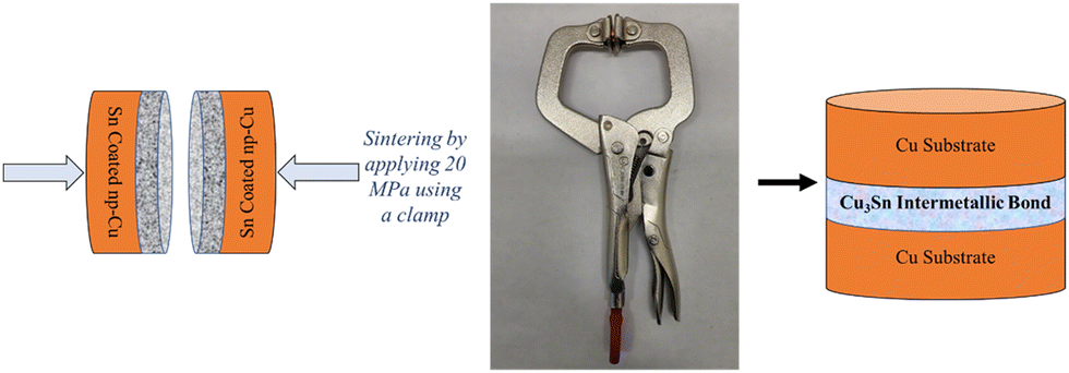
Synthesized np-CuSn films were subjected to sintering processes. Thermal compression bonding was done to realize a densified Cu–Sn intermetallic-based joint. The sintering process was executed by compressing two np-CuSn films (plated on Cu substrates) using C-clamp locking pliers at a bonding pressure of 20 MPa.15Fig. 1 shows the pliers arrangement for the sintering process. The clamped samples were then placed in an OTF-1200X high temperature vacuum tube furnace (MTI Corporation) to realize the sintering process at temperatures of 300 °C for 30 minutes, 250 °C for 30 minutes, 200 °C for 60 minutes, and 180 °C for 60 minutes under forming gas (FG) inert atmosphere. The temperature profile for the sintering process consists of gradually increasing to the desired temperature from ambient condition in 15 minutes, holding the temperature for 60 minutes, then cooling in the same environment for 240 minutes. Prior to the sintering process, np-CuSn film on Cu substrate were dipped in 1 wt% HCl solution for 15 seconds to remove surface oxides.13
 |
| | Fig. 1 Demonstrating the pressure application process, administered at high-temperature, using C-clamp locking pliers. | |
2.4. Characterization
The plated samples (np-CuSn before and after dealloying processes) were characterized by field emission SEM (FEG-SEM Zeiss Supra 55 VP). Top-view in-lens, and secondary-electron (SE2) detectors were used at an accelerating voltage of 15 kV and a working distance of 2–6 mm while using SEM. Cross-sections of the post-sintering formed joints were also imaged using SEM. Prior to imaging, the sintered samples were first embedded in EpoxySet resin then grinded and mechanically polished to expose a cross-section and perfect its surface smoothness, respectively. The cross-sectioned surface was then carbon-coated using a Cressington 208C High Vacuum Turbo Carbon Coater (Ted Pella) prior to SEM imaging. Elemental analyses to obtain atomic compositions were performed via energy dispersive X-ray spectroscopy (EDS) coupled with SEM using the SE2 detector at a working distance of 15 mm and an accelerating voltage of 15 kV. X-ray diffraction (XRD) was also administered to obtain crystallographic profiles of the Cu–Sn films using a Bruker Advanced Diffractometer D8 equipped with a filtered Cu Kα (λ = 1.54 Å) radiation source at the 2θ range of 20–70°. The surface of the np-CuSn films were also characterized by X-ray photoelectron spectroscopy (XPS) using a PHI 5000 Versaprobe Scanning ESCA System with monochromatic Al Kα X-rays of 1486.6 eV (spot size of 200 μm at 50 W, pass energy of 23.5 eV, and takeoff angle of 45° to obtain region scans).
3. Results and discussion
3.1. Voltammetric studies
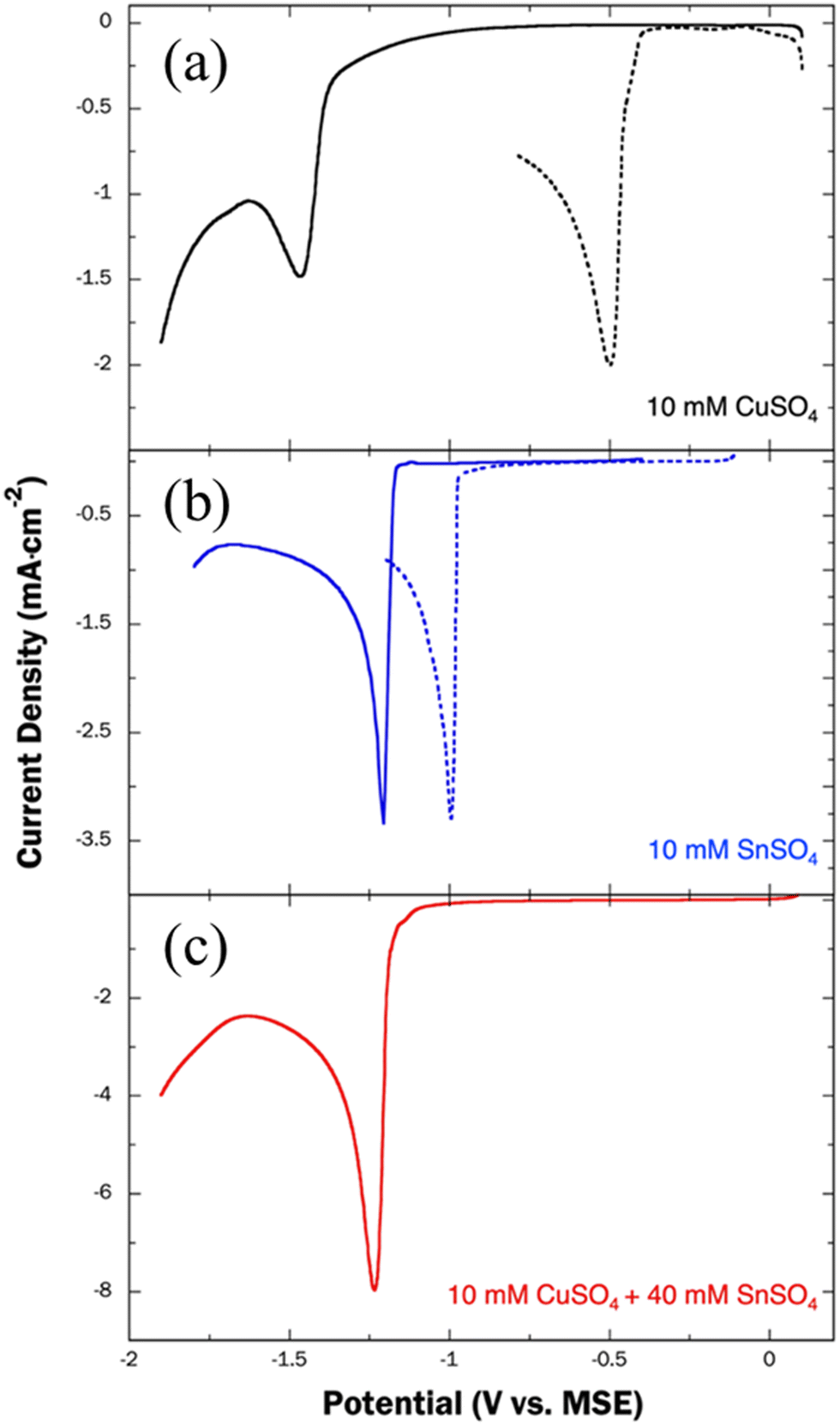
Nanoporous structures are obtained by dealloying of precursor CuSn alloys that contain relatively high amounts of Sn, taking part in those routines as the sacrificial or less noble metal. The electrodeposition of CuSn alloys have been extensively reported in literature, as Cu–Sn alloys are typically used for industrial applications because of their mechanical strength and corrosion resistance.24,25 Typically, CuSn films are produced from baths that include a complexing agent, a vital component for successful co-deposition.26 The citrate ion derived from trisodium citrate salt (Na3Cit) is of key importance among these compounds. It serves as a ligand, shifting the Cu reduction potential closer to that of Sn, thereby enabling co-deposition at similar potentials. To determine the effect of Na3Cit on the reduction potentials of Cu and Sn, cathodic LSVs were performed in the absence and presence of the complexing agent. As seen in Fig. 2a, the onset reduction potential (Eonset) of Cu2+ to Cu0 where an increase of the reduction current density commences, is found at −0.41 VMSE, in the absence of Na3Cit. In the presence of Na3Cit, the Eonset shifts to −1.36 VMSE, reflecting the reduction of Cu-citrate complex. According to theoretical calculations,27 the dominant species participating in the Cu plating process at a bath pH of 6 is the [Cu2Cit2H−2]4− complex is the dominating species taking part in the Cu plating process at pH = 6 (pH of the bath). Others have reported the presence of the [SnCit]2− complex under similar conditions,28 explaining the observed shift in Eonset of Sn/Sn2+ from −0.97 VMSE to −1.17 VMSE, as shown in Fig. 2b. Despite this dynamic interplay, the Eonset difference between Cu and Sn is ultimately reduced from 0.56 V to 0.19 V in the presence of the complexing agent.
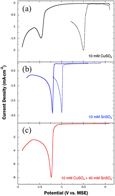 |
| | Fig. 2 LSV curves depicting the cathodic behavior of (a) 10 mM CuSO4 (black curves), (b) 10 mM SnSO4 (blue curves) in the absence (---) and presence (—) of Na3Cit complexing agent and (c) 10 mM CuSO4 + 40 mM SnSO4 (red curve) in the presence (—) of Na3Cit complexing agent. All curves were recorded on Au electrodes at a scan rate of 10 mV s−1. | |
3.2. Electrodeposition of Cu–Sn precursor alloys
Uniformly mixed np-CuSn films were successfully obtained through a process involving the partial dealloying of Sn-rich Cu–Sn alloys, founded on the basics of a previously studied phenomenon known as ‘less noble metal retention’.29,30 A similar approach has previously been reported for the creation of np-AuCu and np-PdCu films, performed via electrochemical etching of pre-deposited Cu-rich Au–Cu and Pd–Cu alloys, respectively.31,32 In theory, the formation of a np-CuSn structure can be realized by selectively removing Sn in an electrolyte that promotes the retention of a certain level of Sn. To this end, Sn-rich (ranging from 65 to 89 at%) CuSn alloys are prepared as precursor substrates through potentiostatic overpotential deposition (OPD) at −1.8 V (vs. MSE). As depicted in the voltammogram in Fig. 2, the Linear Sweep Voltammetry (LSV) of the plating bath, containing a 2![[thin space (1/6-em)]](https://www.rsc.org/images/entities/char_2009.gif) :8 ratio of CuSO4 to SnSO4 in the presence of Na3Cit, reveals a single cathodic peak at −1.24 V (vs. MSE). This peak is attributed to the co-deposition of Cu and Sn. The significant change in current at potentials more negative than −1.65 V indicates the concurrent occurrence of the hydrogen evolution reaction (HER).
:8 ratio of CuSO4 to SnSO4 in the presence of Na3Cit, reveals a single cathodic peak at −1.24 V (vs. MSE). This peak is attributed to the co-deposition of Cu and Sn. The significant change in current at potentials more negative than −1.65 V indicates the concurrent occurrence of the hydrogen evolution reaction (HER).
To obtain Cu–Sn alloys with varying atomic compositions, we employed three deposition baths operating consistently at pH 6, each containing 0.4 M Na3Cit, 0.5 M H3BO3, and different concentrations of CuSO4 and SnSO4 listed in Table 2. At the plating potential of −1.8 VMSE, HER occurs concurrently along with the co-reduction of Cu and Sn, as manifested by the second current density increase in Fig. 2. HER leads to elevated local pH levels in the vicinity of the electrode, resulting in reduced plating efficiency. To mitigate this issue, we introduced as a buffering agent to the bath the aforementioned boric acid.33
Table 2 Elemental composition of electroplated Cu–Sn alloys as determined by EDX; the values in parentheses represent standard deviation
| Bath label |
Bath composition (mM%) |
Alloy atomic% |
| A |
Cu10Sn90 |
Cu10.8Sn89.2(±1.5) |
| B |
Cu20Sn80 |
Cu22.6Sn77.4(±0.9) |
| C |
Cu30Sn70 |
Cu34.6Sn65.4(±2.2) |
We successfully obtained Cu–Sn precursor alloys with three distinct compositions. In each case, the electrodeposited films exhibited a shiny, white appearance akin to that of pure plated Sn. The atomic and weight compositions of these alloys were meticulously determined through Energy Dispersive X-ray (EDX) analysis and are provided in Table 2. It is noteworthy that all bath configurations yielded Sn-rich alloys. In addition, a comparison of the composition of the precursor bath with the atomic compositions of the plated alloys, suggests that the resulting alloy's composition can be fine-tuned by simply adjusting the ratio of the metal ion concentrations in the plating bath.
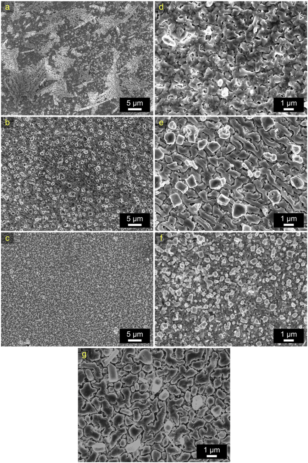
Fig. 3 shows the top-view SEM images of all electroplated CuSn alloys. From these images it can be concluded that the alloys morphologies (Fig. 3a–f) closely resemble the characteristic structure of pure electroplated Sn (Fig. 3g), likely because of the high content of Sn in the alloys. The alloy containing 90 at% Sn shows a flat, plain Sn-like morphology buried underneath three-dimensional (3D) deposits or whiskers that are characteristic of additive-free Sn-plating. Such 3D formations can be avoided by adding to the deposition baths leveling agents – typically organic molecules that absorb to the surface of the deposit.34 Generally, the leveling agents are undesirable additives since they may incorporate into the deposit and then interfere with the sintering process afterwards. However, in the approach of our interest, they are unnecessary since these whiskers targeted for elimination are later removed during the dealloying process. In addition, whisker-free morphologies are observed in the SEM image of the alloy containing 77 at% Sn, with the presence of dominating rectangular and cubic features observed throughout the substrate. Following this trend, smaller feature sizes were obtained in the alloy containing 65 at% Sn, which appears to be uniform throughout the substrate surface.
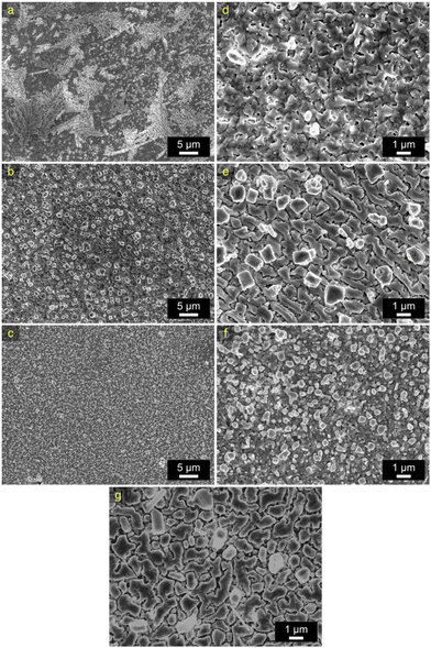 |
| | Fig. 3 Low and high magnification SEM images of Sn-rich Cu–Sn alloys plated using Bath A (a) and (d), Bath B (b) and (e), and Bath C (c) and (f); (g) electroplated pure Sn; figures (a)–(c) were taken at 5000× and figures (d)–(g) were taken at 20000× magnification. | |
3.3. Dealloying of Cu–Sn films – effect of composition of precursor alloy and working substrate
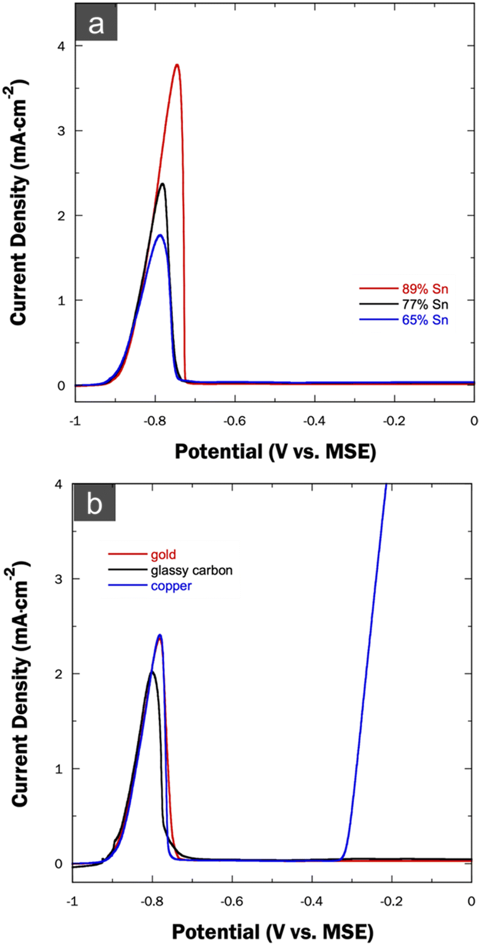
The Sn-rich Cu–Sn precursor alloys detailed in the preceding section underwent dealloying in the second synthetic step via anodic LSV in a sulfate-based solution. In the resulting voltammograms depicted in Fig. 4a, the stripping onset potential consistently appears near −0.90 VMSE and remains constant across all anodic curves, irrespective of the initial alloy composition. The voltammograms exhibit an abrupt drop in current density to nearly 0 mA cm−2 at a potential of −0.72 VMSE, indicating the cessation of further faradaic processes upon proceeding further in the positive direction. The distinguishing factor among various dealloying curves lies in the charge density values, as listed in Table 3, manifested by different peak areas decreasing with the reduction of Sn content in the precursor alloy. It is noteworthy that only a single peak is observed in all dealloying curves despite the anticipated Cu oxidative dissolution at near −0.30 VMSE in this dealloying media. As a result, it is hypothesized that there are alloying trends primarily between Cu and Sn, potentially also involving the Au substrates, which effectively passivates the Cu fraction and prevents it from undergoing oxidation.
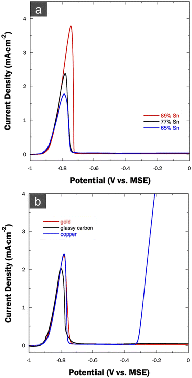 |
| | Fig. 4 (a) LSV curves depicting the partial selective removal of Sn from Cu–Sn alloys (plated on Au surfaces) containing different amounts of Sn as indicated by the figure legend; (b) LSV curves depicting the dealloying of Cu–Sn alloy electrodeposited on different substrates; the voltammograms were recorded in a solution containing 0.1 M Na2SO4 and 1 mM H2SO4 at ν = 1 mV s−1. | |
Table 3 Calculated dealloying charge densities, and atomic composition of dealloyed np-CuSn films as determined by EDX; the values in parentheses represent standard deviation
| Bath label |
Q
dealloy (mC cm−2) |
np-CuSn atomic% |
| A |
518 (±47) |
Cu60.0Sn40.0(±0.5) |
| B |
331 (±19) |
Cu59.3Sn40.7(±2.2) |
| C |
258 (±54) |
Cu60.4Sn39.7(±2.7) |
To assess the validity of this hypothesis, Cu–Sn precursor alloys were electrodeposited on both a Cu substrate and a glassy carbon (GC) substrate, with a fixed alloy composition of Cu22.6Sn77.4. The resulting dealloying curves along with one obtained with the use of Au substrate are presented in Fig. 4b. This absence of additional peaks persists in the case of the GC substrate, where only a single peak is observed, like with the Au substrate., the dealloying curve exhibits a single anodic peak on the Cu substrate at the same position as observed on Au but a notable surge in current density near −0.3 VMSE is also observed and is attributed to the oxidation of the Cu substrate itself. Following this initial peak, a porous structure is obtained as the underlying Cu substrate surface becomes exposed to the dealloying electrolyte and dissolves itself at more positive potentials. Even after that dissolution, the Cu substrate appears to retain a gray np-CuSn layer, suggesting no further dissolution of that layer occurs beyond the first peak. Consequently, it can be inferred that the resulting np-CuSn proves stable on various substrates and is only removable through ‘brute-force’ mechanical polishing of the substrate surface.
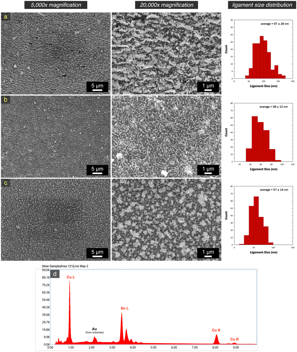
After dealloying in sulfate, all samples transitioned to a darker gray color, a characteristic sign of nanoporosity development.29 This transformation was corroborated through SEM characterization, as illustrated in Fig. 5. Porous structures were observed across all samples, albeit with ligament-pore length scale variation. The structures exhibited relative homogeneity and uniformity throughout the entire substrate, evident in the lower magnification micrographs. The np-CuSn film formed by the dealloying of Cu10.8Sn89.2 (Fig. 5a) showcased continuous ligament networks oriented parallel to each other, featuring an average ligament size of 97 ± 26 nm. Notably, the whisker growth observed earlier in Fig. 4a was absent, indicating that these structures mainly consisted of Sn and as such, were subsequently removed during the dealloying. The np-CuSn film derived from the dealloying of Cu22.6Sn77.4 (Fig. 5b) exhibited the ‘snaky ligament’ characteristic structure with a relatively finer average length scale of 58 ± 12 nm. Furthermore, the Cu34.6Sn65.4 dealloying (Fig. 5c) resulted in a porous structure with a morphology distinct from the two former np-CuSn films. Faceted features were observed along with larger aggregates that developed throughout layers of spherical nanoparticle-like structures. Despite the variation in overall morphology, the average length scale (57 ± 14 nm) was comparable in size to that obtained in Fig. 5b.
 |
| | Fig. 5 Low- and high-magnification SEM micrographs of dealloyed np-CuSn films with precursor alloys containing 89 at% Sn (row a), 77 at% (row b), and 65 at% (row c) and the respective ligament size distribution; (d) representative EDX spectrum of np-CuSn. | |
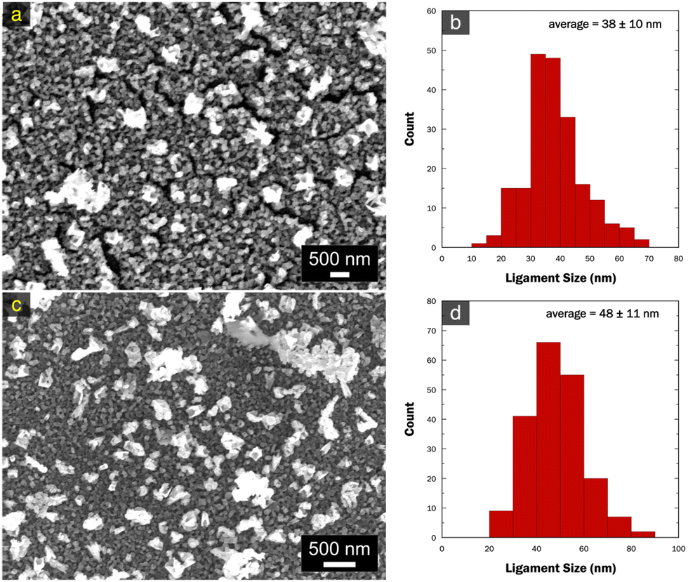
The SEM images of np-CuSn, formed through the dealloying of Cu22.6Sn77.4, on both GC and Cu substrates were also captured (Fig. 6). The micrographs unveil a uniform layer of porous structures with interconnected ligaments, accompanied by some aggregates on the surface. Notably, the ligaments appear relatively denser on the Cu substrate, while more voids were observed on the GC substrate, possibly stemming from the expectedly poorer adhesion of electrodeposits on GC. The average ligament sizes on both GC and Cu substrates are smaller compared to those obtained on Au substrates (Fig. 5).
 |
| | Fig. 6 (a) SEM micrograph of np-CuSn on GC substrate at magnification of 50000× and the respective ligament size distribution (b); (c) SEM micrograph of np-CuSn on Cu substrate at 30000× magnification and the respective ligament size distribution (d). | |
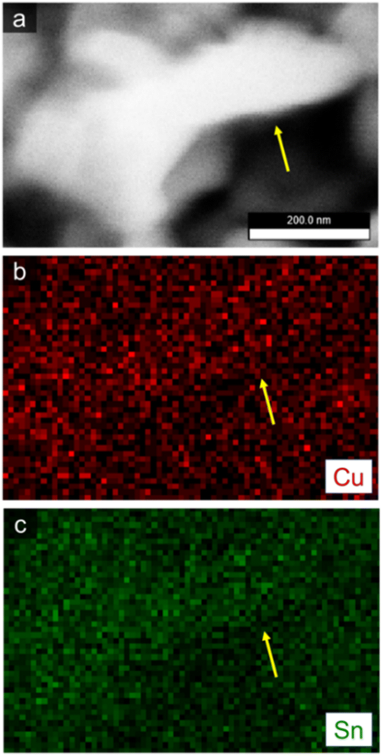
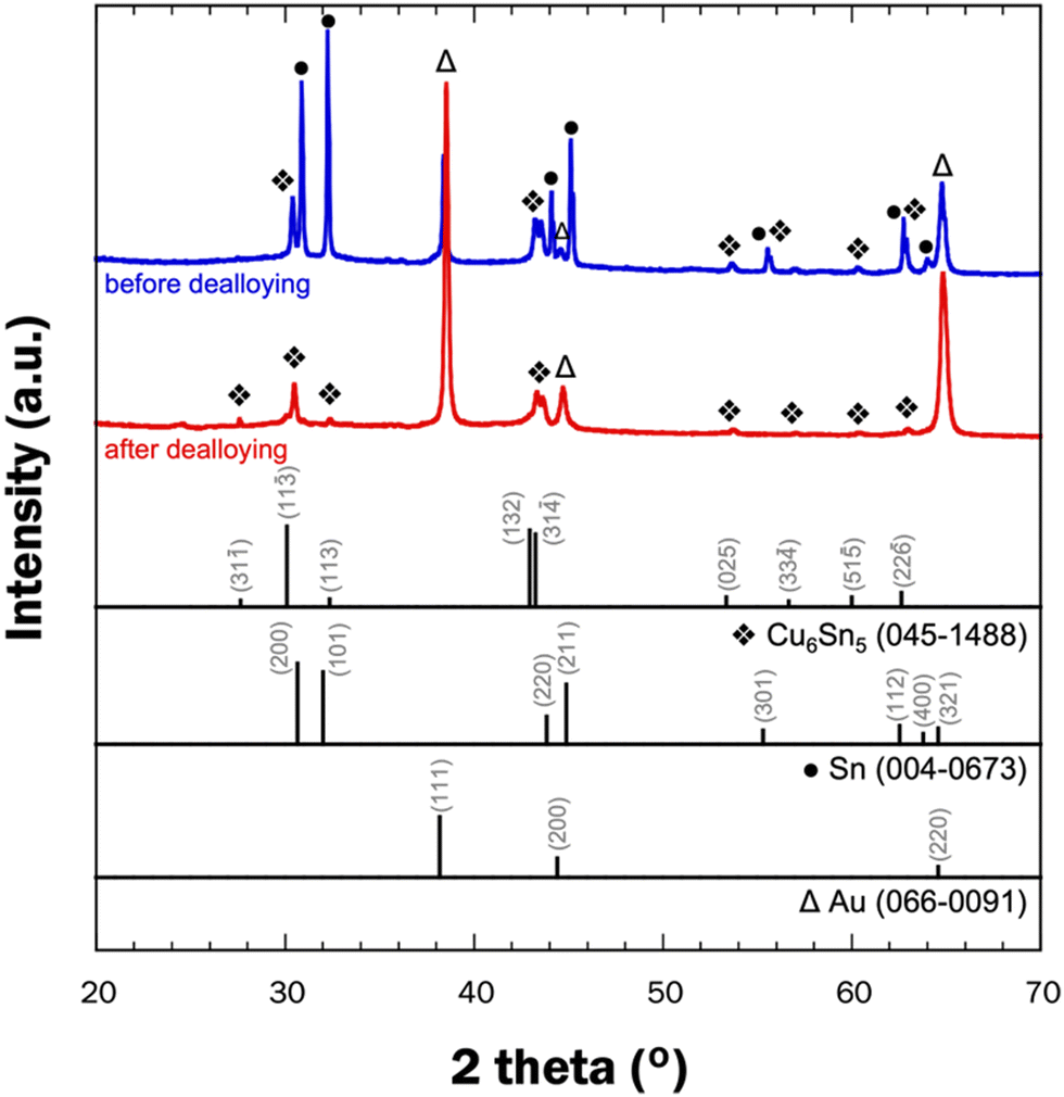
A detailed examination of the overall structure of np-CuSn was conducted through SEM-EDX mapping (Fig. 7), utilizing the Cu K and Sn L edges in the EDX spectrum. The composite maps depict a relatively homogeneous distribution of Cu and Sn. A more focused analysis on a single ligament, indicated by the yellow arrow, reveals a complete mixing of Cu and Sn within the ligament structure. Remarkably, the atomic composition of the np-CuSn films (Table 3) was consistently determined to be approximately Cu60Sn40, irrespective of the precursor alloy composition. This observation suggests that the np-CuSn predominantly comprises the Cu6Sn5 IMC, as this composition range aligns with the dominance of that IMC in the Cu–Sn phase diagram.35 To validate this finding, crystallographic profiles of np-CuSn before and after dealloying were examined through X-ray Diffraction (XRD), and the resulting patterns are presented in Fig. 8.
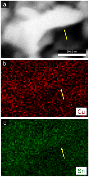 |
| | Fig. 7 High resolution SEM image of np-CuSn and the respective EDX elemental maps of Cu (red) and Sn (green). | |
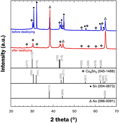 |
| | Fig. 8 XRD patterns of Cu22.6Sn77.4 precursor alloy before and after dealloying. | |
The XRD pattern of the precursor alloy (blue curve) exhibits diffraction peaks corresponding to pure Sn, as anticipated due to the high Sn content in the alloy. Patterns for the Cu6Sn5 IMC are also evident, aligning with expectations from the Cu–Sn phase diagram, which predicts a mixture of Sn and Cu6Sn5 at the atomic composition of Cu22.6Sn77.4 at room temperature.35 Following dealloying (red curve), the characteristic patterns for pure Sn are no longer observed, while those for the Cu6Sn5 IMC persist. This confirmation underscores the presence of the Cu6Sn5 IMC in the np-CuSn structure, maintaining an overall composition of Cu60Sn40, rendering it well-suited for the sintering process. In both patterns, diffraction peaks attributed to Au (from the substrate) were also discernible.
3.4. Dealloying of Cu–Sn films – effect of stripping bath composition
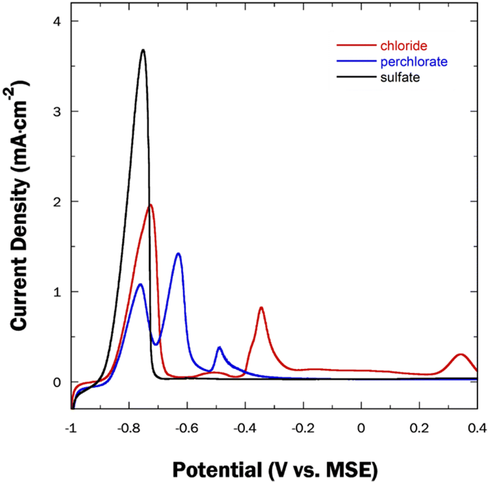
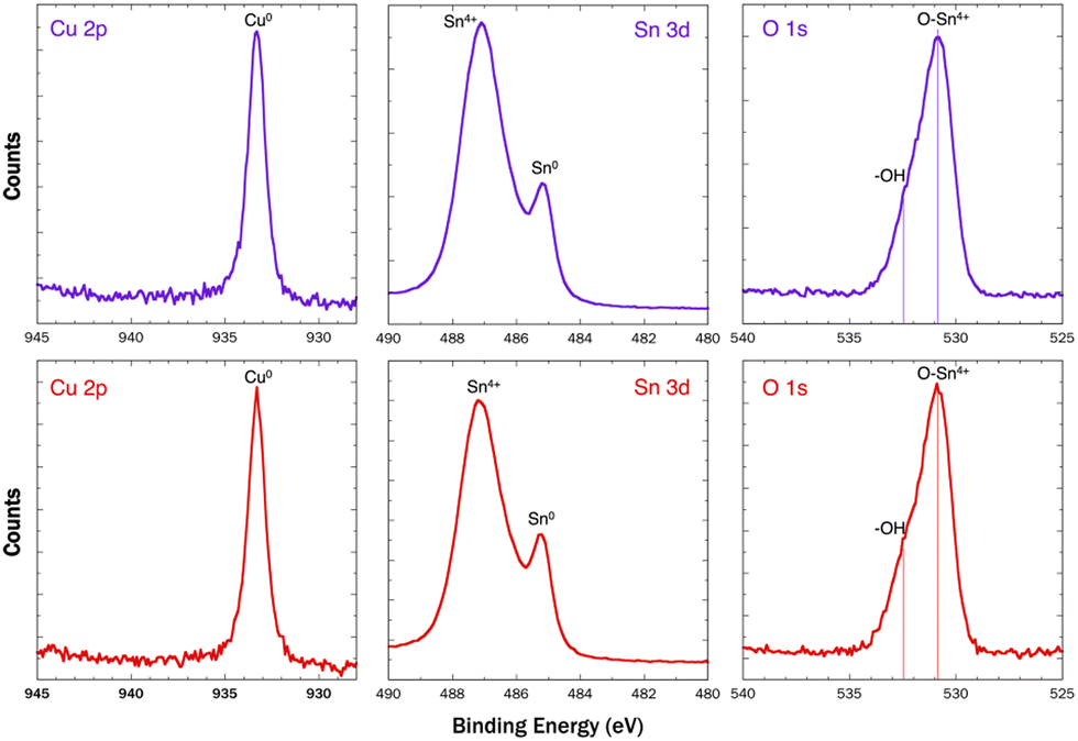
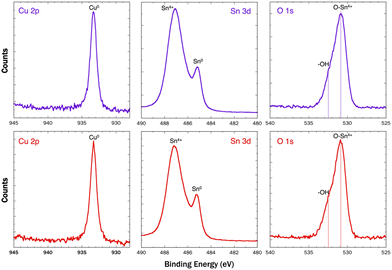
The electrochemical dealloying of Cu–Sn films was further investigated by varying the dealloying bath composition to explore and understand potential passivation of the alloy at more positive potentials. The films were subjected to independent dealloying processes in chloride (0.1 M NaCl, 1 mM HCl) and perchlorate (0.1 M NaClO4, 1 mM HClO4) baths. The resulting voltammograms are displayed in Fig. 9, with the dealloying curve in the sulfate bath included for comparison. As previously mentioned, the dealloying curve of the precursor CuSn alloy in the sulfate bath exhibits a single peak near −0.8 VMSE, corresponding to the selective removal of Sn. In the chloride bath, the same peak at −0.8 VMSE was observed, accompanied by additional features at more positive potentials. This includes a broad peak near −0.5 VMSE, indicating the further oxidation of Sn2+ to a more stable Sn4+ species (eqn (1)). According to the literature, Sn4+ undergoes a hydrolysis reaction in acidic media, leading to the formation of an insoluble Sn(OH)4 compound (eqn (2)), resulting in passivation. It is also reported that high chloride concentrations (exceeding 1 × 10⁻² M) can promote the anodic dissolution of Sn.36,37 However, at these higher concentrations, such as the one used in this study, there is an increase in the [OH−] at the cathode, which leads to the conversion of Sn(OH)4 to [Sn(OH)6]2− (eqn (3)), which may explain the absence of these precipitates on the resulting np-CuSn structure. The presence of adsorbed Sn4+ species was observed in the Sn 3D XPS region spectrum (Fig. 10). The peak at −0.35 VMSE corresponds to the oxidation of Cu.| | | Sn(OH)4 + 2OH− → [Sn(OH)6]2− | (3) |
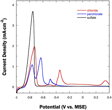 |
| | Fig. 9 LSV curves depicting the oxidation of Cu22.6Sn77.4 alloys in different dealloying baths; the precursor alloys were prepared on Au substrates and were dealloyed at ν = 1 mV s−1. The corresponding arrows indicate the potential cut-offs for dealloying. | |
 |
| | Fig. 10 XPS Cu 2p, Sn 3d, and O 1s (with curve fitting) region spectra of np-CuSn dealloyed in sulfate (purple curves) and in chloride (red curves) baths. | |
Also, previous reports indicate that Cu forms an adsorbed species (eqn (4)) at high chloride concentrations. Once formed this species can be further oxidized to Cu2+ at more positive potentials, which is observed as the fourth peak at +0.34 VMSE.38
| | | CuClads → Cu2+ + Cl−ads + e− | (4) |
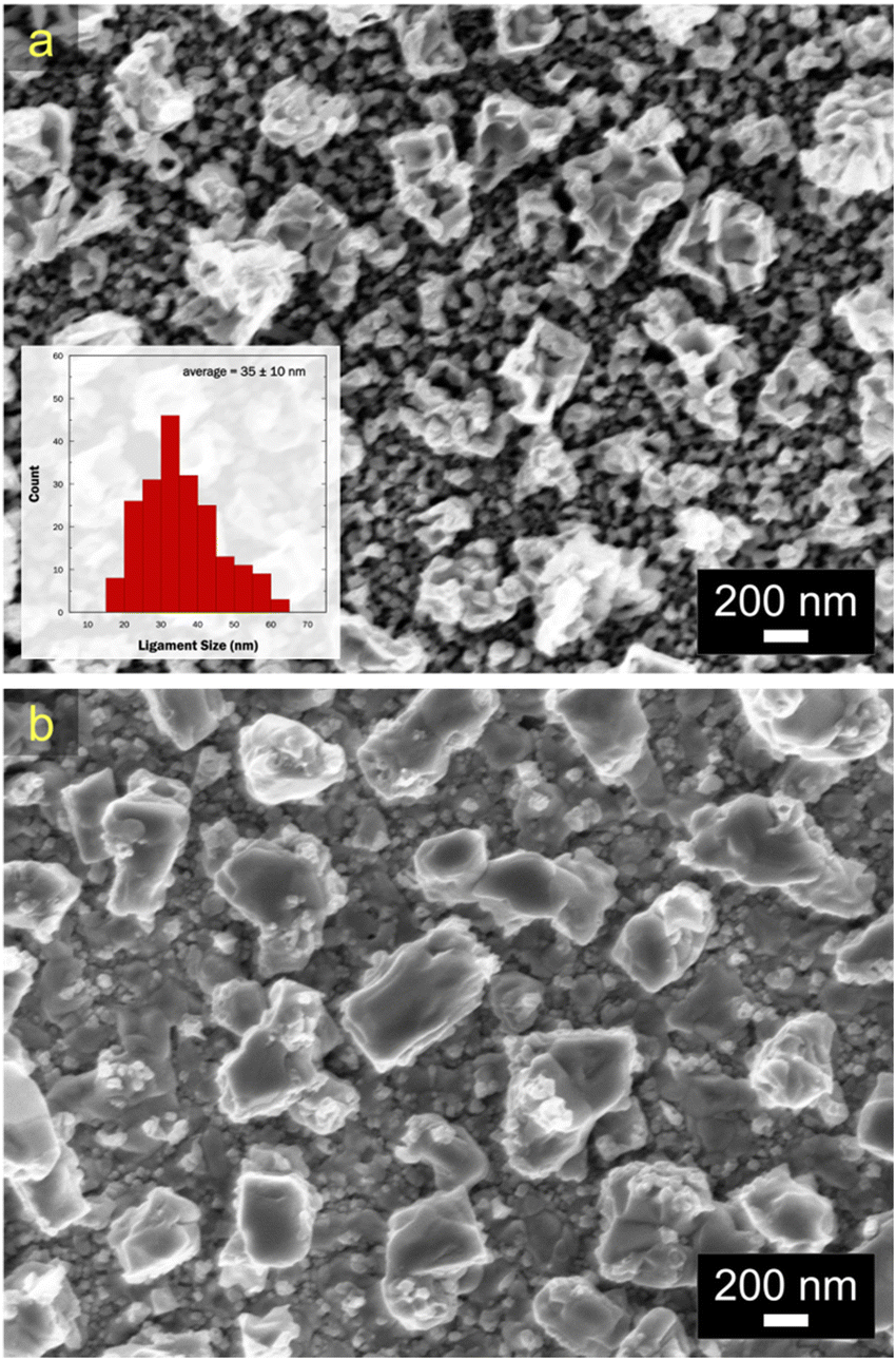
These peak assignments are supported by EDX characterization. Prior to the peak at −0.35 V, the atomic composition of the alloy was Cu51.7Sn48.3, demonstrating the removal of Sn through the first peak (the original composition of the alloy before the dealloying was Cu22.6Sn77.4). Past the peak at +0.34 V, the composition changed to Cu28.7Sn71.3. The XPS region spectrum of Cu 2p showed metallic Cu suggesting that Cu within the np-CuSn matrix was not prone to oxidation. Nonetheless, when the anodic potential scanning was terminated before the first Cu oxidation peak, a np-CuSn structure was also obtained. As seen in Fig. 11a, np-CuSn with an atomic composition of Cu51.7Sn48.3 was observed with finer pore-ligament sizes (average of 35 ± 10 nm). The np-CuSn film synthesized from the chloride bath shows a higher Sn content than the one obtained from the sulfate bath (Cu59.3Sn40.7). This is also supported by the calculated Sn stripping charges, Qstrip, of 199 mC cm−2 and 314 mC cm−2 in the chloride and sulfate solutions, respectively. The adjustability of Sn content in np-CuSn by merely changing the dealloying bath may prove beneficial for sintering at lower temperatures. The XPS region spectrum of Sn for np-CuSn dealloyed in the sulfate bath resembles that obtained in the chloride bath, indicating the presence of Sn4+ species on the surface of the film. Additionally, the O 1s region spectrum was acquired, displaying an asymmetric peak. Fitting of the data revealed the presence of O–Sn4+ lattice oxides and hydroxides on the surface of the np-CuSn structure, aligning with the findings from the Sn 3d region.39
 |
| | Fig. 11 SEM micrographs of Cu–Sn after anodic LSV in (a) chloride and (b) perchlorate baths. Inset in image (a) shows the ligament size distribution of np-CuSn dealloyed in chloride bath. | |
The oxidation of CuSn in the perchlorate bath shows a set of three peaks in the potential range of −0.9 VMSE to −0.3 VMSE. After the second peak, the EDX analysis shows an atomic composition of Cu27Sn71 while a composition of Cu32Sn68 was observed when the potential was scanned up to and past the third peak. Based on the EDX results, it can be concluded that no Cu oxidation occurred, unlike in the case of the chloride bath. This signifies that that set of peaks observed in the perchlorate bath voltammogram is associated with the dissolution and/or oxidation of Sn. However, the lack of substantial morphological (Fig. 11b) and compositional changes (EDX results) after completion of the anodic sweep in perchlorate solution points toward predominant oxidative passivation that preserves both metals in place and leads to the absence surface area development and thereby no of significant increase of the surface-to-volume ratio of accordingly anodized CuSn precursor alloy.
3.5. Sintering of np-CuSn films
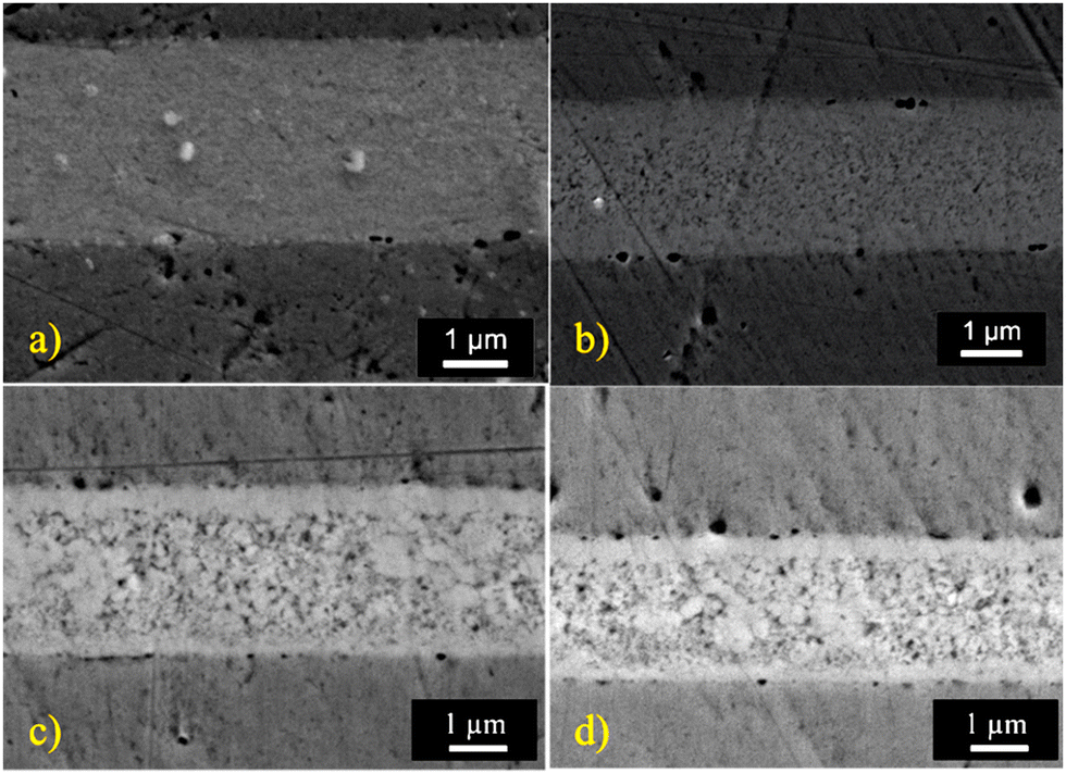
The applicability of np-CuSn films for interconnections of next-generation was evaluated through sintering at 300 °C under a forming gas atmosphere with an applied pressure of 20 MPa. SEM imaging of cross sections (Fig. 12) reveals a fully densified joint with minimal porosity and a thickness of approximately 3 μm. EDX characterization indicates an atomic composition of 75.1 at% Cu and 24.9 at% Sn, consistent with the Cu3Sn IMC, as confirmed by the Cu–Sn phase diagram.35 This newly formed joint exhibits a densified configuration alike with observed in previous research.15 Characterizations and previous observations15 suggest that during sintering, the high pressure and rapid heating cause Cu from the substrate to diffuse into the np-Cu6Sn5 bonding material, ultimately converting it to Cu3Sn. Notably, Cu3Sn IMC possesses a lower resistivity of 8.3 μΩ cm compared to Cu6Sn5 (17.5 μΩ cm).21,22 The np-Cu6Sn5 solderability was also assessed by lowering sintering temperatures to 250 °C for 30 minutes, 200 °C for 60 minutes, and 180 °C for 60 minutes, while maintaining a pressure of 20 MPa. The atomic composition of the accordingly generated joints closely matched Cu3Sn, indicating that np-Cu6Sn5 can form joints down to lower temperatures than most traditional methods, also ensuring consistency in the formation of Cu3Sn-based joints across varying temperatures. As depicted in Fig. 12 the resulting joints exhibit well-densified IMCs. Notably, there is a discernible decreasing trend in density as the temperature decreases. Nevertheless, these joints display significantly less porosity when compared to those formed by nano-Cu paste. Despite the initial high porosity of the np-Cu6Sn5 film, all joints exhibit properties closely matching the characteristics of their bulk bonding material counterparts, such as conventional and microjoints, formed at the Cu-solder interface in electronic packaging.40,41
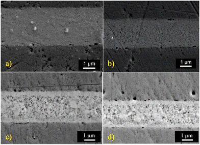 |
| | Fig. 12 Cross-sectioned SEM micrographs of joints formed by sintering np-CuSn at (a) 300 °C, (b) 250 °C, (c) 225 °C and (d) 180 °C. | |
3.6. Accelerated aging test
Semiconductor materials must operate at elevated temperatures while sustaining high current density, presenting challenges related to reliability in solder joints and other bonding materials.42,43 Interconnection nodes in these devices typically consist of ultra-fine pitch Cu-solder-Cu microbumps enriched with Sn. The primary component of these solder microbumps is Sn, which forms a thin layer of Cu3Sn IMC in the Cu interface, succeeded by a thicker layer of Cu6Sn5 IMC. However, studies have indicated that Cu3Sn and Cu6Sn5 IMCs are susceptible to Kirkendall effect that creates vacancies and promotes the growth of micrometer-size voids at the Cu–Cu3Sn interface. Over time or prolonged exposure to elevated temperatures that accelerates the growth of Cu3Sn and Cu6Sn5 IMC layers, these voids grow further, thus compromising both mechanical resilience and current-carrying capability. Interestingly, it has been observed that in the absence of the Cu6Sn5 layer, voiding does not occur in the Cu/Cu3Sn interface.15
Accelerated aging testing on our sintered joints has been conducted to explore this phenomenon.41,44Fig. 13 presents SEM cross-section images of an np-CuSn film sintered at 180 °C and then annealed at 200 °C for 120 h and 168 h. Comparing these cross sections with the untreated one in Fig. 12d reveals a consistent absence of void formation dynamics at the Cu/Cu3Sn interface. This result aligns with our previous findings in another paper, where similarly generated joints showed no void formation even under extended heat treatment.15 These images reaffirm the hypothesis that the completion of the Cu6Sn5 conversion to Cu3Sn during the sintering process results in joints with a stable Cu3Sn IMC content. Consequently, the annealing process does not induce the diffusion of extra Cu or Sn, preventing the creation of a Kirkendall imbalance that could promote potential void formation and growth. Instead, the observed trend during heat treatment is the coalescence of pores inherited from the structure of the original np-CuSn bonding material. In summary, thermal aging does not lead to the formation of voids in the intermetallic joints.15
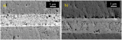 |
| | Fig. 13 Cross-sectioned SEM micrographs of joints aged for (a) 120 h and (b) 168 h at 200 °C. | |
4. Conclusions
This research has successfully demonstrated the viability of bimetallic nanoporous materials as cutting-edge bonding materials for electronic packaging. Through the development of an optimized approach involving potentiostatic deposition, we have achieved the synthesis of a Cu–Sn precursor alloy. The selective removal of Sn from that alloy allowed for the synthesis of a nanoporous CuSn film with a high surface-to-volume ratio and a targeted atomic composition closely resembling the Cu6Sn5 IMC. The np-CuSn film underwent a high-pressure sintering process at various temperatures (300 °C, 250 °C, 200 °C, and an unprecedented 180 °C), resulting in the formation of densified joints with minimal porosity. Notably, this study marks the first successful achievement of a sintering temperature as low as 180 °C for Cu3Sn IMC joints. Furthermore, the results of accelerated aging tests underscore the robust nature of these joints, with no void formation detected throughout the aging process. This compelling evidence serves to reinforce recent advancements in the creation of dependable and low-temperature interconnections within electronic devices. The innovative methodology outlined in this study carries substantial potential in influencing the trajectory of electronic packaging materials and processes. Hopefully, these findings will be of significant interest to both the research and professional communities.
Author contributions
E. Castillo: conceptualization, literature review, methodology, resources, data curation, validation, investigation, visualization, writing – original draft; A. F. Pasha: visualization, resources, methodology, data curation, validation; Z. I. Larson: data curation, visualization, N. Dimitrov: supervision, conceptualization, visualization, project administration, funding acquisition; all authors took part in the writing – review & editing the manuscript.
Conflicts of interest
The authors declare no competing financial interest.
Acknowledgements
This work was supported by the Semiconductor Research Corporation through the Center for Heterogeneous Integration Research on Packaging Task 2878.011. E.C. also thanks the Chemistry Department at Binghamton University for additional support through the Dissertation Fellowship. The authors also acknowledge Peter Borgesen and his research group for their assistance with the sintering experiments, and Krystal J. Lee her help with the XRD.
References
- R. Gao, J. Shen, F. Xie, Y. Zuo and D. Wu, J. Electron. Mater., 2017, 46, 6388–6394 CrossRef CAS.
-
H. Lai, Y. Zhang, G. Yang, C. Cui and S. Ta, Study on the Interconnect Performance of Multicomponent paste for 3rd Generation Semiconductor Packaging, presented in part at the 2020 21st International Conference on Electronic Packaging Technology (ICEPT), Guangzhou, China, 2020, pp. 1–4, DOI:10.1109/ICEPT50128.2020.9201927.
-
P. Liu, Fundamentals of Electromigration in Interconnects of 3D Packaging, in 3D Microelectronic Packaging: From Fundamentals to Applications, ed Y. Li and D. Goyal, Springer International Publishing, Cham, 2017, pp. 223–244, DOI:10.1007/978-3-319-44586-1_9.
- K. Mohan, N. Shahane, R. Liu, V. Smet and A. Antoniou, JOM, 2018, 70, 2192–2204 CrossRef.
-
K. Croes, C. Adelmann, C. J. Wilson, H. Zahedmanesh, O. V. Pedreira, C. Wu, A. Leśniewska, H. Oprins, S. Beyne, I. Ciofi, D. Kocaay, M. Stucchi and Z. Tőkei, Presented in part at the 2018 IEEE International Electron Devices Meeting (IEDM), 2018, 5.3.1–5.3.4 Search PubMed.
- K. Schnabl, L. Wentlent, K. Mootoo, S. Khasawneh, A. A. Zinn, J. Beddow, E. Hauptfleisch, D. Blass and P. Borgesen, J. Electron. Mater., 2014, 43, 4515–4521 CrossRef CAS.
- J. Li, Q. Liang, T. Shi, J. Fan, B. Gong, C. Feng, J. Fan, G. Liao and Z. Tang, J. Alloys Compd., 2019, 772, 793–800 CrossRef CAS.
-
B. H. Lee, M. Z. Ng, A. A. Zinn and C. L. Gan, Presented in part at the 2015 IEEE 22nd International Symposium on the Physical and Failure Analysis of Integrated Circuits, 2015, 102–106 Search PubMed.
- S. Thekkut, M. Z. Kokash, R. S. Sivasubramony, Y. Kawana, K. Mirpuri, N. Shahane, P. Thompson, C. M. Greene and P. Borgesen, J. Electron. Packag., 2021, 144, 03100101 Search PubMed.
-
N. Shahane, K. Mohan, G. Ramos, A. Kilian, R. Taylor, F. Wei, P. M. Raj, A. Antoniou, V. Smet and R. Tummala, Presented in part at the 2017 IEEE 67th Electronic Components and Technology Conference (ECTC), 2017, 968–975 Search PubMed.
-
N. Shahane, K. Mohan, R. Behera, A. Antoniou, P. R. Markondeya, V. Smet and R. Tummala, Presented in part at the 2016 IEEE 66th Electronic Components and Technology Conference (ECTC), 2016, 829–836 Search PubMed.
-
K. Mohan, N. Shahane, R. Sosa, S. Khan, P. M. Raj, A. Antoniou, V. Smet and R. Tummala, Presented in part at the 2018 IEEE 68th Electronic Components and Technology Conference (ECTC), 2018, 301–307 Search PubMed.
-
R. A. Sosa, K. Mohan, L. Nguyen, R. Tummala, A. Antoniou and V. Smet, Presented in part at the 2019 IEEE 69th Electronic Components and Technology Conference (ECTC), 2019, 655–660 Search PubMed.
- M. Njuki, S. Thekkut, R. Das, N. Shahane, P. Thompson, K. Mirpuri, P. Borgesen and N. Dimitrov, J. Appl. Electrochem., 2022, 52, 259–271 CrossRef CAS.
- E. Castillo, M. Njuki, A. F. Pasha and N. Dimitrov, Acc. Chem. Res., 2023, 56, 1384–1394 CrossRef CAS PubMed.
- E. Roduner, Chem. Soc. Rev., 2006, 35, 583–592 RSC.
- M.-S. Kim and H. Nishikawa, J. Mater. Sci. Eng. A, 2015, 645, 264–272 CrossRef CAS.
- Y. Zuozhu, F. Sun and M. Guo, Mater. Res. Express, 2018, 5, 086503 CrossRef.
- A. Arazna, A. R. Królikowski, G. Koziol and J. Bieliński, Mater. Corros., 2013, 64(10), 914–925 CrossRef CAS.
- W.-L. Chiu, C.-M. Liu, Y.-S. Haung and C. Chen, Mater. Lett., 2016, 164, 5–8 CrossRef CAS.
- P. Yao, X. Li, X. Han and L. Xu, Soldering Surf. Mount Technol., 2018, 31, 6–19 CrossRef.
- S. K. Kang, W. K. Choi, M. J. Yim and D. Y. Shih, J. Electron. Mater., 2002, 31, 1292–1303 CrossRef CAS.
- J. Erlebacher, M. J. Aziz, A. Karma, N. Dimitrov and K. Sieradzki, Nature, 2001, 410, 450–453 CrossRef CAS PubMed.
- Y. Sürme, A. A. Gürten, E. Bayol and E. Ersoy, J. Alloys Compd., 2009, 485, 98–103 CrossRef.
- M. Karthik, J. Abhinav and K. V. Shankar, Met. Mater. Int., 2021, 27, 1915–1946 CrossRef CAS.
- W. H. Qi and M. P. Wang, Mater. Chem. Phys., 2004, 88, 280–284 CrossRef CAS.
- G. Heidari, S. M. Mousavi Khoie, M. E. Abrishami and M. Javanbakht, J. Mater. Sci.: Mater. Electron., 2015, 26, 1969–1976 CrossRef CAS.
- C. Han, Q. Liu and D. G. Ivey, Electrochim. Acta, 2009, 54, 3419–3427 CrossRef CAS.
- Y. Liu, S. Bliznakov and N. Dimitrov, J. Electrochem. Soc., 2010, 157, K168–K176 CrossRef CAS.
- D. Artymowicz, Z. Coull, M. Bryk and R. Newman, ECS Trans., 2011, 33, 1 CrossRef CAS.
- Y. Xie, C. Li, E. Castillo, J. Fang and N. Dimitrov, Electrochim. Acta, 2021, 385, 138306 CrossRef CAS.
- Y. X. Xie and N. Dimitrov, Appl. Catal., B, 2020, 263, 118366 CrossRef CAS.
- A. Lopalco, A. A. Lopedota, V. Laquintana, N. Denora and V. J. Stella, J. Pharm. Sci., 2020, 109, 2375–2386 CrossRef CAS PubMed.
- Y. Goh, A. S. M. A. Haseeb and M. F. M. Sabri, Electrochim. Acta, 2013, 90, 265–273 CrossRef CAS.
- S. Fürtauer, D. Li, D. Cupid and H. Flandorfer, Intermetallics, 2013, 34, 142–147 CrossRef PubMed.
- X. Zhong, G. Zhang, Y. Qiu, Z. Chen, W. Zou and X. Guo, Electrochem. Commun., 2013, 27, 63–68 CrossRef CAS.
- M. Jafarian, F. Gobal, I. Danaee, R. Biabani and M. G. Mahjani, Electrochim. Acta, 2008, 53, 4528–4536 CrossRef CAS.
- W. Shao, G. Pattanaik and G. Zangari, J. Electrochem. Soc., 2007, 154(7), D339–D345 CrossRef CAS.
- M. Kwoka, B. Lyson-Sypien, A. Kulis, D. Zappa and E. Comini, Nanomaterials, 2018, 8, 738 CrossRef PubMed.
- Y. H. Liu, L. Yin, S. Bliznakov, P. Kondos, P. Borgesen, D. W. Henderson, C. Parks, J. Wang, E. J. Cotts and N. Dimitrov, IEEE Trans. Compon. Packag. Technol., 2010, 33, 127–137 CAS.
- M. Njuki, S. Thekkut, R. Sivasubramony, C. M. Greene, N. Shahane, P. Thompson, K. Mirpuri, P. Borgesen and N. Dimitrov, Mater. Res. Bull., 2022, 150, 111759 CrossRef CAS.
- M. Njuki, S. Thekkut, R. Das, N. Shahane, P. Thompson, K. Mirpuri, P. Borgesen and N. Dimitrov, J. Appl. Electrochem., 2022, 52, 259–271 CrossRef CAS.
-
S. Thekkut, R. Das, M. Njuki, J. Li, R. S. Sivasubramony, F. W. Alshatnawi, M. Moise, C. M. Greene, N. G. Dimitrov, P. Borgesen, N. Shahane, P. Thompson and K. Mirpuri, Presented in part at the 2020 Ieee 70th Electronic Components and Technology Conference (ECTC 2020), 2020, 485–491 Search PubMed.
- X. Peng, Y. Wang, Z. Ye, J. Huang, J. Yang, S. Chen and X. Zhao, J. Mater. Sci.: Mater. Electron., 2022, 33, 25753–25767 CrossRef CAS.
|
| This journal is © The Royal Society of Chemistry 2024 |
Click here to see how this site uses Cookies. View our privacy policy here. 
 Open Access Article
 This Open Access Article is licensed under a Creative Commons Attribution-Non Commercial 3.0 Unported Licence
 *
*