DOI:
10.1039/D3MA01033C
(Paper)
Mater. Adv., 2024,
5, 2110-2119
Atomistic insights into predictive in silico chemical vapor deposition
Received
21st November 2023
, Accepted 8th January 2024
First published on 10th January 2024
Abstract
An unmatched atomistic technique for predictive in silico chemical vapor deposition (CVD) is reported from an experimental and modeling perspective in the current manuscript. The gas-phase and surface-phase chemical reaction rates dependent on the precursor's flow rates, reactor chamber geometry, and other input conditions are observed to play significant roles in deciding the monolayer growth morphology. The randomness-based kinetic Monte Carlo (kMC) technique is exploited for the computation of adsorption, diffusion, and desorption rates. The deposition of silicon (Si) and silicon-germanium (SixGe1−x) layers over the 〈100〉 Si substrate is carried out to measure the thin film quality, growth rate, strain, lattice constant, and mole-fraction and map the point defects (vacancies) along with the surface roughness. The impact of variation of various input physical parameters is studied during the validation of experimental results. The growth rates of Si and SixGe1−x are found to be in good agreement with the experimental results under the similar input conditions. The common natural phenomenon of self-organization of spontaneously formed spatial, temporal, or spatio-temporal patterns is observed during growth through the proposed technique.
Introduction
The chemical vapor deposition (CVD) reaction process for homo and hetero-epitaxy on single-crystal surfaces involves the following mechanisms: transportation of reaction gases into the reaction chamber; formation of intermediate reactants from reactant gases; diffusion of reactant gases through the gaseous boundary layer to the substrate; adsorption of gases onto the substrate surface; single or multi-step reactions at the substrate surface; desorption of product gases from the substrate surface; and forced exit of product gases from the system.1–12
The computational solution of the problem associated with length scales around micron and time scales of the order of seconds is impossible through any numerical method. The computational fluid dynamics (CFD) method uses continuum model equations (Navier–Stokes) to predict the deposition process without any knowledge of atomistic scale information.13
The epitaxial growth of silicon as a function of surface temperature (570–770 °C) exploiting the kinetic Monte Carlo (kMC) technique is reported by Vivien et al.14 Juan et al. reported lattice kinetic Monte Carlo technique for reproducing the epitaxial growth of silicon using H2/SiH4 chemistry for the prediction of growth rates based on surface chemical kinetics.15 The review on the computational Si and SiGe CVD epitaxy throws light on the latest updates till date.16 The lattice kinetic Monte Carlo (LkMC) method reported in the ref. 14–16 uses two approaches, i.e., on-lattice kMC and off-lattice kMC methods. The on-lattice kMC method is where all the bonding positions over the lattice are predefined.17 This method is incapable of predicting information regarding strain, various types of defects and their formation mechanisms, and other physical parameters, which are required to understand the growth morphology. On the other hand, the off-lattice kMC method is more complex than the on-lattice method; however, incorporating elastic effects into kMC simulations in a way that could retain simplicity has emerged as a central challenge in the off-lattice mode.17 The impact of the CVD reactor geometry and precursor diffusivity on the chemical kinetics is totally ignored in all these previously reported studies.
In the current study, the authors have attempted to address the above issues through the in-house developed algorithms in form of TNL-EpiGrow simulator to handle the coupled reactor geometry dependent chemical kinetics and kinetic Monte Carlo (kMC) technique. It uses CVD reactor geometry dependence on the precursors’ flow along with coupled gas- and surface phase chemical kinetics. The atoms bonding is decided by the hybridization rule, which itself find the bonding position following the natural phenomenon of the growth process in the real reactor environment. The proposed technique is innovative and significantly differs from the previously reported on-lattice and off-lattice models. The difference can be accounted in terms of the position of atoms, which are not fixed here as the case of the on-lattice model and does not spend much time on locating the local minima and saddle points to make the bond as in the case of the off-lattice model. The surface grows like an actual sample with atoms taking position according to their bond angles and distances. The capabilities to map each and every deposited atoms over the lattice layer-by-layer make it possible to extract the lattice parameters, mole fraction, strain, dislocations, defects (point, line, and stacking faults, misfits etc.), and roughness.9,10
The proposed technique has capabilities to reproduce the real-time experimental data in case users have calibrated the CVD reactor process. Deeper insight and control over the chemical kinetics and growth morphology can be achieved. On the other hand, where users have no access to experimental data or the process is new, means no information regarding the process; the TNL chemical kinetics module with forward and reverse reactions rates help to estimate the accurate flux inside the reactor. TNL-Optimizer helps to run design of experiments with minor variation in the Ehrlich–Schwoebel and nearest neighbor energies barriers itself to obtain high-quality films with minimum defect densities, roughness, etc. The optimum growth rate obtained under the above conditions produced by the TNL-optimizer guides the experimental design to get the deposition information with the deeper insight. The proposed technique in the form of the TNL-EpiGrow simulator is tested and verified for other groups IV–IV, III–V, and II–VI semiconductors on choosing a substrate other than Si. TNL-EpiGrow simulator has flexibility to incorporate user-defined materials as the substrate and coating materials.17–19
Technique
The CVD reactor-based epitaxial growth of Si and SixGe1−x materials over the Si(100) substrate are predicted with the help of coupled chemical kinetics and kMC method.1–12
The chemical kinetics provides useful predictions regarding chemical reactions probabilities of the particular gas phase reaction in terms of the activation energy and the limiting steps of surface phase reactions. These two terms are essentially important for the proper understanding of deposition processes.20–24 However, the rigorous kinetic analysis with the probability of several reaction paths is crucial for the better understanding of the chemical vapor deposition (CVD) processes, including the adsorption and desorption events over the substrate surface.
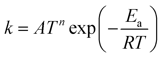
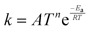
TNL chemical kinetics utility package is designed to facilitate the simulations of the elementary gas and surface phase chemical reactions under CVD process systems to help a user work efficiently with large systems of chemical reactions and develop representations of systems of equations that define a particular problem. The reaction rate constant of the reactions is generally assumed to have the following modified Arrhenius temperature dependence17,18
| | 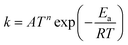 | (1) |
where
Ea(cal) is the activation energy and is often identifiable with the energy barrier for some actual process to occur,
e.g., breaking of a bond. Here,
T refers to the gas temperature,
n is the temperature exponent, and
R is the universal gas constant.
17,18 The coefficient
A is known as the pre-frequency factor and is dependent on the entropy of formation. The prefactor
A (unit is dependent on the order of reaction) also includes information regarding the random motion of molecules as they vibrate, rotate, and translate inside the CVD reactor space and take part in the computation of the thermal energy of the molecules as per the transition state theory (TST). The temperature distribution inside the CVD chamber plays a significant role in the decision of particular gas phase reactions.
Atoms are deposited at random on a periodic array of adsorption sites at the rate of F per site (the deposition flux); these atoms diffuse across the surface, leading to nucleation and growth; subsequently, the atoms are deposited on the top of these layers and either diffuse to their edges and descend (often with some inhibition due to the presence of an Ehrlich–Schwoebel step-edge barrier to downward transport25,26) or nucleate new islands in higher layers. A step-edge barrier thus induces the formation of stacks of atoms. The kinetic Monte Carlo (kMC) technique is exploited to compute the adsorption, diffusion, and desorption rates. The rates of each event help in calculating the total rate and are given as.17,19,27
Here,
A,
H, and
D are the adsorption, diffusion, and desorption rates, respectively. The adsorption rate is measured as the number of interacting adsorbed atoms per unit site per unit time. Hopping rate (
H) is the likelihood of an atom moving to its neighboring site, while desorption rate (
D) refers to the sum of different desorption rate of atoms from the CVD chamber.
The in-house developed technique (in form of TNL-EpiGrow simulator) couples the chemical reactions kinetics in the gas- and surface-phase with the kMC method along with the impact of reactor geometry.17–19 The Si and SiGe CVD process details are given in three subsections.
I. Influence of CVD reactor geometry
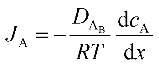
The reactant flux according to Fick's law, is computed as| | 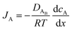 | (3) |
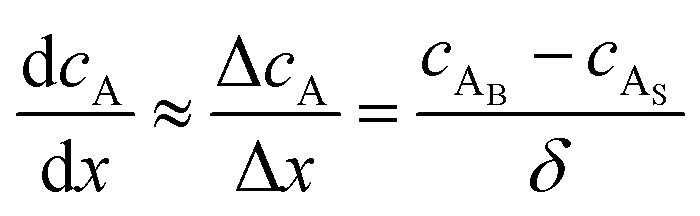
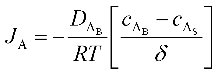
where JA is the diffusion flux of species A, DAB is the diffusivity of the bulk stream reactants, cA is the concentration of species A, x is the direction perpendicular to the substrate surface, R is the gas constant, and T is the absolute temperature. The concentration gradient is approximated as| | 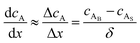 | (4) |
where cAB and cAS are the bulk stream concentration and surface concentration of species A, respectively. δ is the chamber boundary layer thickness. The reactant diffusion through the boundary layer is computed as follows.| | 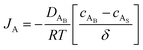 | (5) |
The binary diffusivity, DAB, of the reactants dependent on Leonard-Jones parameters (σ, Ω) is calculated through the Chapman–Enskog theory5–8| | 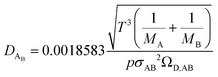 | (6) |
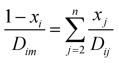
where T is the absolute temperature, M is the molecular weight, p is the pressure, σAB is the collision diameter, and ΩD,AB is the collision integral and dependent on temperature and intermolecular potential. Multi-precursors system in the proposed method is handled by considering an effective binary diffusivity for each species through the gas mixture. The reactant diffusivity in the gas mixture is determined from the mass fraction as| |  | (7) |
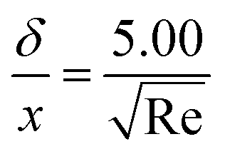
where xi is the mole fraction of the ith species, Dim is the effective binary diffusivity for the diffusion of i in a mixture, and Dij is the binary diffusivity for the diffusion of i in j. Laminar gas flow is taken in the CVD reactor. The reactant concentrations and gas velocity are taken as zero at the substrate surface and increase to the bulk concentration and bulk stream velocity at some distance δ from the substrate surface, which is given by ref. 5–8.| |  | (8) |
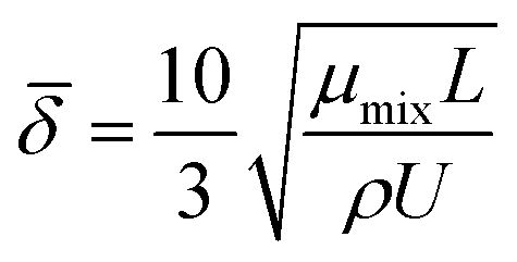
The average boundary layer thickness, δ, is computed by integrating eqn (8) over the length of the substrate and dividing the output by the length of the substrate.| |  | (9) |
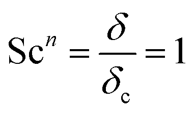
Here, L is the length of the substrate, ρ is the gas density, μmix is the viscosity of the gas mixture, and U is the free stream velocity. In case when the gases are well mixed at minimal temperature gradients, the diffusion path is determined by the concentration boundary layer, δc, which is related to the momentum boundary layer. It is characterized by a Schmidt number of unity as follows.| |  | (10) |
The viscosity of a gas mixture, μmix, is computed as| | 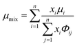 | (11) |
where, 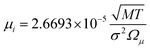 and
and| | 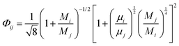 | (12) |
where n is the number of chemical species, xj are the mole fractions of species i and j, M is the molecular weight, T is the absolute temperature, σ is the collision diameter, Ωμ is the collision integral for viscosity, xi and xj are the mole fractions of species i and j, and Mi and Mj are the molecular weights of i and j, respectively.
II. Chemical reaction kinetics
The gas- and surface-phases Arrhenius parameters are listed in Table 2.
a. Silane.
Silane gas is used for the silicon (Si) epitaxial growth with the possible decomposition reaction routes. It decomposes into SiH2 and H2. SiH2 reacts with SiH4 to form Si2H6 in the gas phase. The disilanes (Si2H6) decompose by the elimination of hydrogen (H2) with the formation of HSiSiH3, an intermediate compound. The possibility of the decomposition of HSiSiH3 into H2SiSiH2 is also considered in present analysis.25 The surface phase reactions consider the adsorption of SiH4, SiH2, and H2 molecules over the Si substrate. SiH4 itself decomposes into SiH3 → SiH2 → SiH and finally into Si with H2 abstraction in each decomposition over the substrate surface. The hydrogen adsorption–desorption equilibrium is crucial because hydrogen adsorption competes with silane for occupying the free available surface sites on the substrate lattice22.
b. Disilane.
Similarly, disilane is other most preferred precursor gas used for Si epitaxial deposition.2,22
c. Germane.
SixGe1−x, growth is carried out using silane and germane as the main precursor's gases along with H2 as the carrier gas.23,24
III. Kinetic Monte Carlo technique
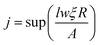
The adsorption, hopping, and desorption rates are computed with the help of eqn (2). The anisotropic kinetics due to the surface reconstruction has dealt with the randomness of the kMC method. The surface kinetics is totally dependent on randomness, energy, and surface temperature. The adsorption rate is measured as the number of interacting adsorbed atoms per unit site per unit time. Since this rate is identical at every site on the surface, the total adsorption rate is thus given as follows.17,18Here, A denotes the total adsorption rate, F denotes incident atomic or molecular flux over the substrate surface, and l and w denote length and width of substrate, respectively.
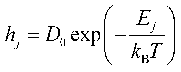
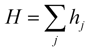
The diffusion or hopping rate (H) is the likelihood of an atom moving to its neighboring site. This is described through the Arrhenius relation.
| | 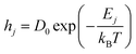 | (14) |
Here,
hj is the hopping rate of the
jth atom,
Ej is the activation energy of the
jth atom and its unit is in eV,
kB is the Boltzmann constant in eV, and
T is the substrate temperature (K). The pre-factor
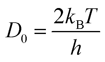
D0 corresponds to vibration frequency, which can be obtained by the application of the equipartition theorem. The characteristic vibration frequency
D0 is given as follows.
17,18| |  | (15) |
where
kB is Boltzmann's constant and
h is Planck's constant.
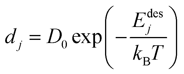
The desorption rate (D) is taken as the sum of different desorption rates of atoms. One atom desorption rate can be described by Arrhenius relation and is given as follows.17,18
| |  | (16) |
Here,
dj is the desorption rate of the
jth atom,
Edesj is the activation energies responsible for desorption of the
jth atom and dependent on the nearest neighbor energies as well, and
T is the substrate temperature (K). The activation energies are generally different for each atom. Its calculation is based on the assumption that bonds only exist between the nearest neighboring atoms. Denoting
Es as the surface diffusion energy barrier,
En is the nearest binding energy and
n is the number of nearest neighbors (n–n) on the surface. The total activation energy is thus computed as follows.
17,18The proposed technique has capabilities to reproduce the types of growth modes itself without the use of any continuum models,
i.e., Stranski–Krastanov (SK), Volmer–Weber (VW), and Frank–van der Merwe growth models. Refer to
eqn (17); the growth mechanism is only dependent on the nearest neighbor (
En), surface (
Es) energies, and the lattice parameters of the substrate and coating film. The role of various energies of each and every atom on the surface decides the type of growth,
i.e., layer-by-layer or island-based growth.
Except for n–n interaction, other effects that are also responsible for activation energies such as step-edge barriers from descending steps in the form of Schwoebel–Ehrlich barrier and ascending steps in the form of incorporation barrier are also relevant in surface diffusion and are given in Table 2.
Thus,
and
Here,
Es and
En describe the surface and nearest neighbor energies, respectively. The Schwoebel and incorporation barriers energies are represented by
Eshw and
Ei respectively. The barrier energy is dependent on the sites on the lattice; hence, the activation energy of the same atom is also dependent on the sites available for diffusion on the lattice.
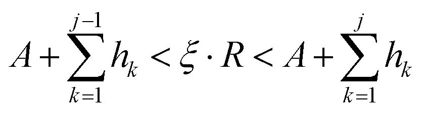
The total hopping rate is calculated by  . The total absorption (A) and hopping (H) rates are dependent on the sites available on the lattice. The rates of each type of event transitions (R) are calculated by eqn (2).
| |  | (19) |
where
τ denotes the time interval of an event, and
ξ is a random number uniformly distributed between 0 and 1. The selection of any event is a random process in kMC algorithms, controlled by a uniformly distributed random number
ξ.
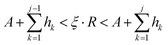
For the deposition event, the total transition rate R multiplying ξ must be smaller than the total adsorption rate A, i.e.,
Otherwise, the diffusion or hopping event takes place if
ξ·
R is not smaller than
A. The desorption event takes place when the atom absorbs energy equal to the desorption energy.
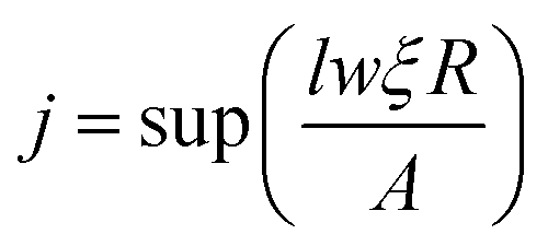
The flux is assumed to be the same for all the sites on the lattice; we may easily find the adsorption site by
| |  | (21) |
where the lateral size of simulation surface
l and
w are measured by unit cell and
j reveals the deposition site from one of the
lw sites. In case of diffusion, due to the different hopping rates for different atoms, the hopping sites are calculated as follows.
| |  | (22) |
Here,
j represents the diffusing atom number.
In case of sp3 hybridization, the bonds among atoms have tetrahedral orientations, i.e., when an atom makes bond with another atom, it follows tetrahedral bond angles between them, and the rest of the bonds also follow this angle arrangement. This is where the term patches came from; it only recognizes the tetrahedral bonding position and angles.17 The values of θ1 and θ2 are computed by the adaption of the model proposed in ref. 17. The model promotes the self-assembly of structures to be grown by the kMC method.17 The complete kMC flow chart of algorithms implemented inside the EpiGrow simulator and the surface roughness are given in ref. 17. The proposed epigrowth technique is also tested and verified with other semiconductors of groups IV–IV, III–V, and II–VI on substrates other than Si.
Results and discussion
An attempt to reproduce the in silico CVD process through the simulation for Si and SiGe deposition respectively reported in ref. 28 and 29 over the Si substrate with crystallographic orientation (100) is carried out successfully by validating the growth rates under similar conditions.
In case of Si deposition, silane and disilane precursors with constant flow rate of 45 sccm were used, whereas for SiGe deposition, the silane and germane precursors with flow rate of 10 sccm and 1 sccm are used, respectively. The partial pressure of carrier gas H2 is taken as 1 slm in both cases. The various geometrical parameters associated with the CVD chamber and type of precursors and their flow rates listed in Table 1 are taken from ref. 28 and 29 along with the various other physical parameters used in the epitaxial deposition simulation of the silicon (Si) and silicon-germanium (SixGe1−x) layers. The values of various energy barriers, i.e., surface energy (eV), nearest neighbor energy (eV), Schwoebel barrier (eV), incorporation barrier (eV), and desorption barrier (eV), are used here as the free parameters. These values are optimized by the running design of experiments (DOE) to calibrate the experimental growth rates.28,29
Table 1 Various physical parameters used for the epitaxial deposition of silicon (Si) and silicon-germanium (SixGe1−x) layers
| Parameters |
Si |
SixGe1−x |
| Chamber temperature (°C) |
550–80021 |
600–70022 |
| Chamber pressure (Torr) |
1021 |
8022 |
| Cross sectional area (cm2) |
1221 |
1222 |
| Length of chamber (cm) |
10021 |
10022 |
| Distance between substrate and edge (cm) |
1.021 |
1.022 |
| Precursors |
SiH4/Si2H6 |
SiH4 & GeH4 |
| Precursors flow rate (sccm) |
4521 |
10 & 122 |
| Carrier gas |
H2 |
H2 |
| Carrier gas flow rate (sccm) |
10![[thin space (1/6-em)]](https://www.rsc.org/images/entities/char_2009.gif) 00021 00021 |
1000022 |
| Substrate temperature (°C) |
80021 |
80022 |
| Surface energy (eV) |
2.0 |
2.0 |
| Desorption barrier (eV) |
3.0 |
3.0 |
| Schwoebel barrier (eV) |
0.05 |
0.05 |
| Incorporation barrier (eV) |
0.05 |
0.05 |
| Nearest neighbor energy (eV) |
0.05 |
0.05 |
| No. of interactive elements |
1 |
1 |
Table 2 Gas phase (G) and surface phase (S) reversible and irreversible reactions are considered for Si deposition from silane. The rate constant is taken as  with units in terms of mol, cm, s, cal, and K. Surface rate (ks) is in cm2 mol−1 s−1, gas rate (kg) is in cm3 mol−1 s−1.14 * and σ represent adsorbed species and free surface site, respectively
|
|
Reaction |
Phase |
A
|
n
|
E
a (cal) |
| Silane |
Gas |
|
|
SiH4 ↔ SiH2 + H2 |
G1 |
3.1 × 10+09 |
0.7 |
54710 |
|
|
SiH4 + SiH2 ↔ Si2H6 |
G2 |
1.8 × 10+10 |
1.7 |
50200 |
|
|
Si2H6 ↔ H2 + HSiSiH3 |
G4 |
9.1 × 10+09 |
1.8 |
54200 |
|
|
HSiSiH3 + SiH4 ↔ SiH2 + Si2H6 |
G4 |
1.7 × 10+14 |
0.4 |
8900 |
|
|
HSiSiH3 + H2 ↔ SiH2 + SiH4 |
G5 |
2.5 × 10+13 |
−0.2 |
5380 |
|
|
HSiSiH3 ↔ H2SiSiH2 |
G6 |
9.3 × 10¹³ |
0.0 |
4092 |
|
|
Surface |
|
|
SiH4 + 2σ → SiH3* + H* |
S1 |
9.3 × 10+13 |
0.5 |
3000 |
|
|
SiH3 + σ → SiH2* + H* |
S2 |
1.1 × 10+19 |
0.0 |
27000 |
|
|
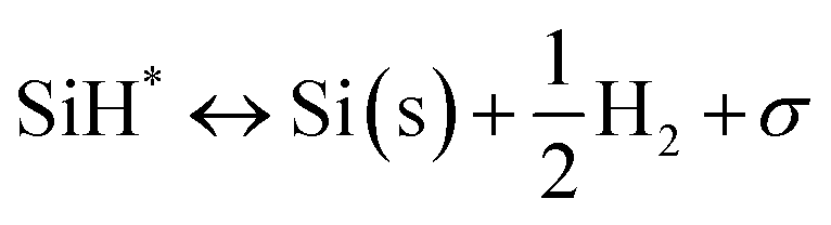
2SiH2* → 2SiH* + H2 |
S3 |
4.4 × 10+17 |
0.0 |
45000 |
|
|
SiH2 + σ→SiH2* |
S4 |
2.4 × 10+24 |
0.5 |
0 |
|
|
|
S5 |
5.8 × 10+11 |
0.0 |
47000 |
|
|
2H* → H2 + 2σ |
S6 |
7.9 × 10+11 |
0.0 |
43000 |
|
|
H2 + 2σ → 2H* |
S7 |
1.3 × 10+22 |
0.5 |
17250 |
| Disilane |
Gas |
|
|
Si2H6 ↔ SiH2 + SiH4 |
G1 |
3.1 × 10+09 |
0.7 |
54710 |
|
|
Si2H6 ↔ H2 + HSiSiH3 |
G2 |
9.1 × 10+09 |
1.8 |
54200 |
|
|
HSiSiH3 + SiH4 ↔ SiH2 + Si2H6 |
G3 |
1.7 × 10+14 |
0.4 |
8900 |
|
|
SiH4 + SiH2 ↔ Si2H6 |
G4 |
1.8 × 10+10 |
1.7 |
50200 |
|
|
HSiSiH3 + H2 ↔ SiH2 + SiH4 |
G5 |
2.5 × 10+13 |
−0.2 |
5380 |
|
|
HSiSiH3 ↔ H2SiSiH2 |
G6 |
9.3 × 10¹³ |
0.0 |
4092 |
|
|
Surface |
|
|
SiH4 + 2σ → SiH3* + H* |
S1 |
9.3 × 10+13 |
0.5 |
3000 |
|
|
SiH3 + σ → SiH2* + H* |
S2 |
1.1 × 10+19 |
0.0 |
27000 |
|
|
2SiH2* → 2SiH* + H2 |
S3 |
4.4 × 10+17 |
0.0 |
45000 |
|
|
SiH2 + σ → SiH2* |
S4 |
2.4 × 10+24 |
0.5 |
0 |
|
|
|
S5 |
5.8 × 10+11 |
0.0 |
47000 |
|
|
2H* → H2 + 2σ |
S6 |
7.9 × 10+11 |
0.0 |
43000 |
|
|
H2 + 2σ → 2H* |
S7 |
1.3 × 10+22 |
0.5 |
17250 |
| Germane |
Gas |
|
|
GeH4 ↔ GeH2 + H2 |
|
3.09 × 1009 |
1.3 |
54700 |
|
|
Surface |
|
|
GeH4 ↔ Ge + H2 |
|
1.15 × 10¹⁹ |
0.33 |
3000 |
|
|
GeH2 ↔ Ge+H2 |
|
5.75 × 10¹¹ |
0.33 |
0 |
|
|
H2 + σ ↔ 2H* |
|
2.29 × 10¹¹ |
0.5 |
17250 |
The proposed technique is competent to extract various physical properties and provides deeper insights into the CVD process at the atomic scale.
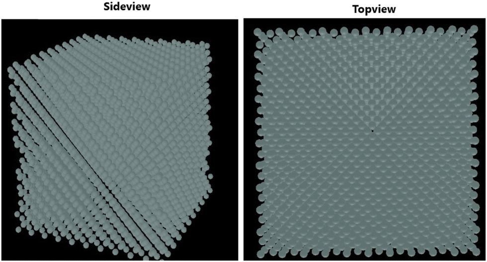
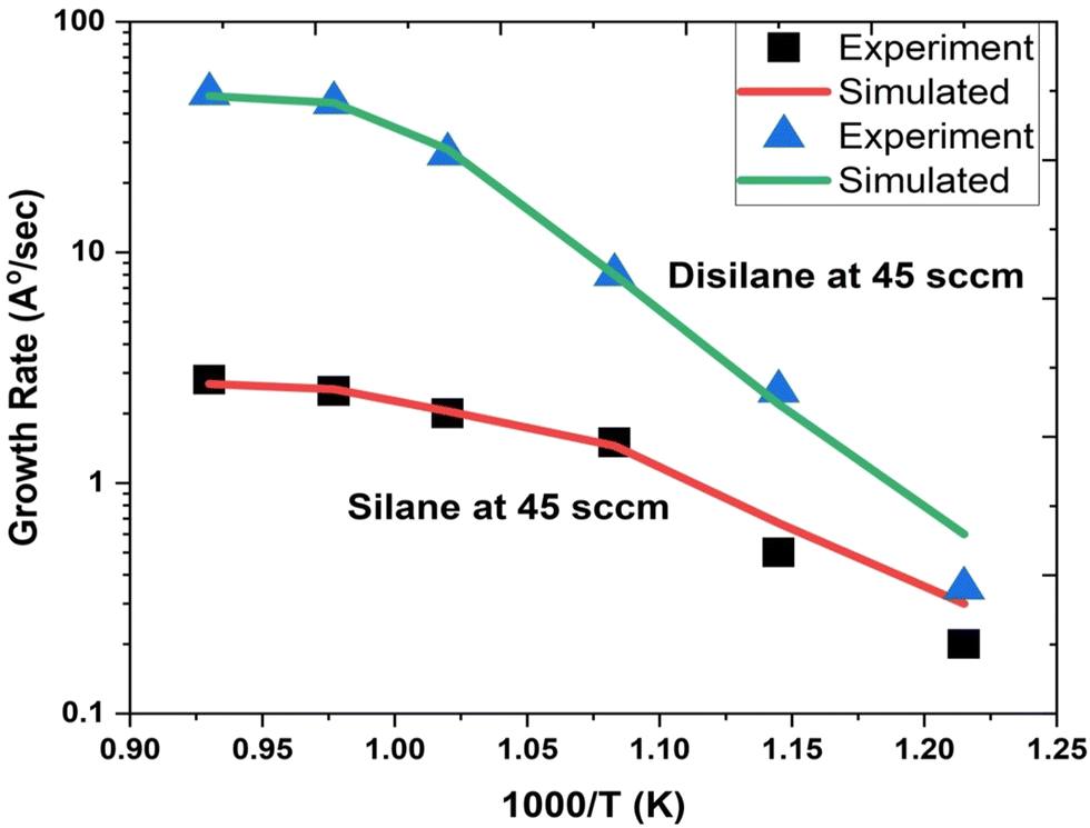
Fig. 1 depicts the epitaxial atomistic scale Si thin film side view and top view; atoms are deposited over the Si(100) substrate. The unit cell of Si is taken as a group of four bonding atoms in tetrahedral phase symmetry. The cluster of unit cells in a row is treated as a single monolayer. The number of layers is counted from the figure. The number of layers deposited is found to be dependent on the partial pressure of the precursor gases, i.e., with the increase in the partial pressure of the precursor gases, the number of layers increases. The two case studies for silane (SiH4) and disilane (Si2H6) gases with constant flow rate 45 sccm are taken as precursor gases for the deposition of Si. The Si substrate with crystallographic orientation (100) is used for the deposition of Si in both cases. The substrate temperature is kept constant (800 °C) during the entire growth mechanism, whereas the CVD chamber temperature is varied from 550 to 800 °C. The growth rate of each case as a function of inverse CVD chamber temperature is shown in Fig. 2. The atomistic Si deposition is carried out at 550–800 °C temperature range. It is observed that below the chamber temperature 550 °C (not shown here) in both cases, the growth rates are negligible or diminished, which is explained in terms of chemical kinetics. It is well known phenomena that CVD process is a thermal process and temperature invokes the chemical reactions kinetics inside the chamber. The dissociation temperature of silane and disilane is 525 °C and 500 °C, respectively. Therefore, at Tcham < 550 °C, the decomposition of silane and disilane is negligible; the growth rates are negligible in both cases. The growth rates of Si using silane and disilane precursors separately in the temperature ranges 660—780 °C and 700–780 °C are observed to be limited by the mass transport regime, as reflected from the figure (i.e., at x-axis range 0.95–1.075 for silane and 0.94–1.028 for disilane, respectively). The growth rate in the mass transport regime is almost constant. The gas phase reactions kinetics play a significant role to decide the atomic transport regimes. The impact of substrate orientation on the mass transport limited growth rates are observed to be negligible. On the other hand, the kinetics-limited process in the case of silane and disilane under temperature is in the range of 550–660 °C and 550–700 °C (i.e., at x-axis range 1.072–1.215 for silane and 1.028–1.215 for disilane), respectively, over the substrate surface is observed to be strongly dependent on the crystallographic orientation of the substrate. There are many studies on the orientation dependence of harpooning in gas-phase reactions, and a striking effect of orientation on the dynamics of vibrational energy transfer is elaborated in detail; refer to ref. 30. The temperature is varied from 550 to 800 °C, i.e., at higher temperature range (∼660–780 °C), the impact of mass transport regime is observed, whereas under lower temperature range (∼550–700 °C), the surface kinetics reactions limited process dictates the growth rates. The silane and disilane dissociation rate at higher temperature increases with an increase in temperature, resulting in more flux at the surface as compared to lower temperature. It also causes a significant change in the growth rates by affecting the surface adsorption, hopping, and desorption rate probabilities due to change in the surface composition. The growth steeply decreases under the surface kinetics reactions limited region. The adsorption, hopping, and desorption rates are also dependent on the number, nature, and configuration of surface sites, bonds, and features (steps, kinks, ledges, vacancies, etc.) at the substrate. The role of various energy barriers treated as free parameters (e.g., surface, Schwoebel barrier, incorporation, desorption, and nearest neighbor) during the calibration of the experimental result have shown significant contribution in the prediction of the growth morphologies. Each energy barrier values are optimized by running virtual design of experiments (VDOE) to match the experimental growth rate. The growth rates in each case, i.e., for silane (SiH4) and disilane (Si2H6) precursors separately at constant partial pressure 45 sccm, are matched with the experimental rates reported by Adam et al.28 The absolute matching between the simulated and experimental Si growth rate is achieved as shown in Fig. 2. It justifies the validity and reliability of the proposed technique for Si CVD growth.
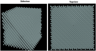 |
| | Fig. 1 Side view and top view of the deposited layered structure of the Si thin film over Si substrate. | |
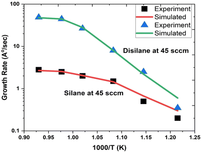 |
| | Fig. 2 The comparison of the simulated and experimental growth rates as a function of inverse temperature. The growth rate using silane precursor (45 sccm flow rate) separately with carrier gas H2 flow rate (1 slm) shown by solid red line (simulated) and black square symbols (experimental taken from ref. 28. The growth rate using disilane precursor (45 sccm flow rate) separately with carrier gas H2 flow rate (1 slm) shown by solid green line (simulated) and blue triangle symbols (experimental taken from ref. 28. | |
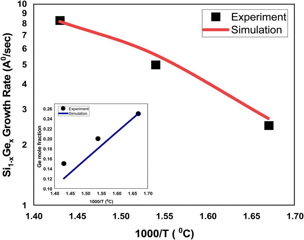
The growth rate of epitaxially-deposited thin film of SixGe1−x using silane (SiH4) and germene (GeH4) precursors with flow rates in the ratio 10:1 to obtain the desired mole fraction of Ge is depicted in Fig. 3. The CVD chamber temperature is varied in the temperature ranges of 600–700 °C, whereas the substrate temperature is kept constant, i.e., 800 °C. The pressure of the CVD chamber is set to 80 Torr. The growth rate of SixGe1−x using silane and germane precursors as a function of temperature is calibrated with the experimental rate reported by Tillack et al.29 by treating various energies barriers as free parameters (e.g., surface, Schwoebel barrier, incorporation, desorption, and nearest neighbor). The barrier energies play a significant role in achieving the bond-making conditions. The sticking coefficient of the particular atom and molecule dictate the probability of the adsorption rate. The hopping or diffusion rates of atoms and molecules over the substrate surface are found to be dependent on the substrate orientation and temperature. Higher substrate temperature imparts more thermal energy to the adsorbed atoms and molecules over the substrate surface. The probability of the high diffusion rates increases the time to make the bonds with the substrate atoms. A number of adsorbed atoms and molecules are desorbed from the substrate surface depending upon the desorption barrier energy value. The growth rate of SixGe1−x is shown in Fig. 3. The absolute matching between simulated (solid line) and experimental growth rate (symbol) result evidently again justifies the feasibility and validity of the proposed atomistic CVD growth technique. The inset curve shows the comparison between the simulated Ge mole-fraction with the experimental one. The inset figure shows the corresponding linear decrease in the mole fraction (x) of germanium in Si1−xGex thin film with an increase in the chamber temperature. Under constant chamber pressure, the variation in chamber temperature from 600 °C to 700 °C is responsible for the decomposition of germene. At higher temperature, the gas phase decomposition of germene is more probable compared to the lower temperature regime. Therefore, the mole-fraction of Ge increases with the increase in the chamber temperature, which is evident from the inset figure of Fig. 3. The addition of Ge atoms into the Si lattice is observed to be strongly dependent on the substrate temperature also. The addition of germane precursor causes an increase in the hydrogen desorption process over the substrate and increased growth rate is observed. The simulated growth rate and mole fraction are in good agreement with the experimental results.29
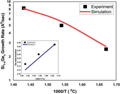 |
| | Fig. 3 The comparison of the simulated and experimental growth rates for the SiGe deposition as a function of inverse temperature. The simulated growth rates are shown by solid red (silane and gemane precursors used) line, whereas experimental growth rates29 are depicted by black square (silane and gemane precursors used) symbols. The flow rates of the silane and gemane precursors are taken as 10 sccm and 1 sccm for SiGe deposition, whereas H2 flow rate is taken 1 slm. The content of Ge in the SiGe film is shown in the inset figure and compared against the experimental data.29 | |
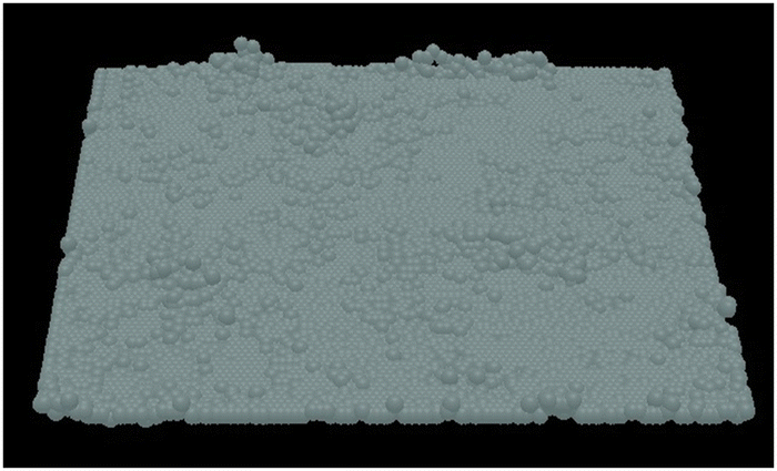
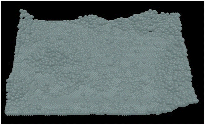
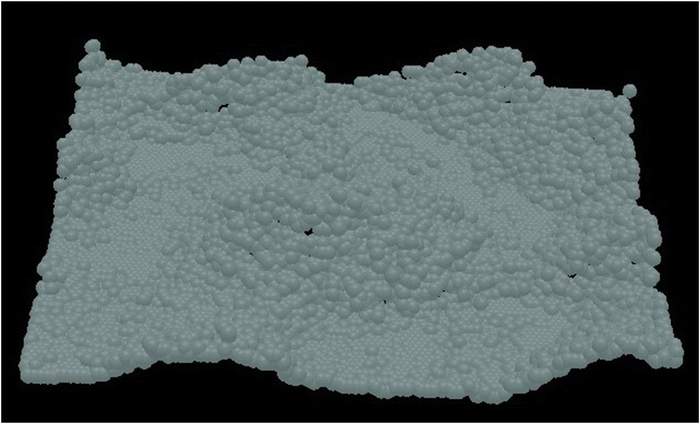
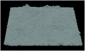
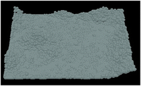
The comparison of surface profiles after 10 s, 20 s, and 30 s growth of Si over 54.3 × 54.3 nm2 Si substrate are shown in Fig. 4–6, respectively. From Fig. 4, it is clearly reflected that atomistic growth shows layer-by-layer pattern and is dependent on the surface and nearest neighbor energies. However, the transition from layer-by-layer to island-based growth occurs after a critical layer thickness is achieved, which is shown in Fig. 5, and island-based growth mode is reflected in Fig. 6. The transition from layer-by-layer to island-based growth justifies the experimental Stranski–Krastanov (S–K) growth mode. The island's radius are extracted in the range of 8–12 nm.
 |
| | Fig. 4 Surface profile after 10 s growth shows layer-by-layer growth. | |
 |
| | Fig. 5 Surface profile after 20 s growth (transition from layer-to-layer to island mode growth). | |
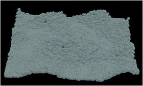 |
| | Fig. 6 Surface profile after 30 s growth justifies the experimental Stranski–Krastanov mode growth (island mode growth). | |
The lattice feature is depicted in terms of variation of the surface roughness, as shown in Fig. 7. The nature of roughness curves with respect to increasing growth time for the Si and SixGe1−x thin films shows almost similar behavior. It is clearly seen from Fig. 2 and 3 that the surface roughness curves during the first 10 s increases sharply and then show saturation behavior in both the Si case. The behavior of the surface roughness curves for Si and SixGe1−x is explained on the basis of the arrival of number of atoms and available vacant sites density on the substrate surface. Initially, the roughness curves increase steeply because the density of atoms reaching the substrate sites are dependent on the reversible chemical reaction kinetic rate, start from zero, and increase until and unless the forward reaction rate of reversible reactions attained equilibrium. As compared to the Si case, low surface roughness values are shown by the SixGe1−x case. However, it increases with respect to the growth time. The high decomposition rates of GeH4 generate more flux as compared to SiH4 under similar conditions. The increase in the surface roughness value with respect to the growth time is attributed to the incorporation of Ge atoms into Si monolayers. The difference in the radius of Ge atoms and Si atoms, i.e., RGe > RSi (RGe = 1.225 Å, RSi = 1.11 Å) is responsible for increasing the surface roughness an increase in the growth time.
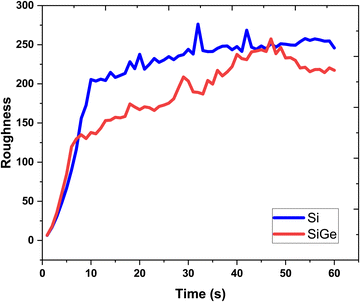 |
| | Fig. 7 The surface roughness extracted each second of the growth time. | |
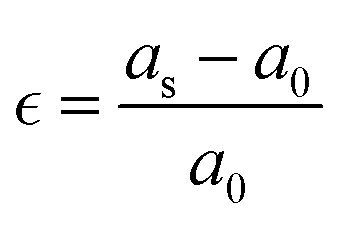
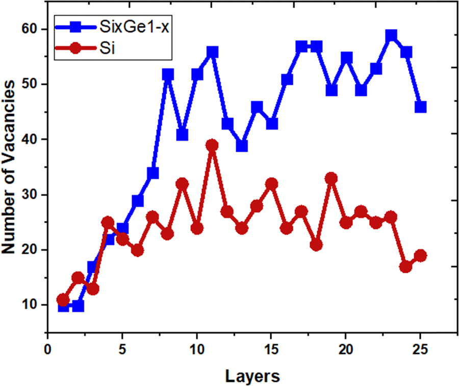
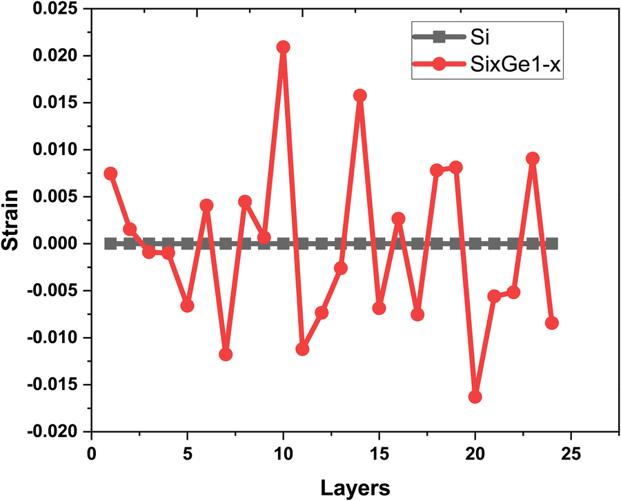
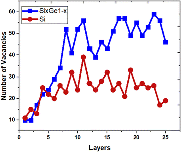
The vacancies density in each layer of Si and SiGe thin films, which are extracted by tracing each bonding sites in the lattice, are shown in Fig. 8. The lattice sites where no atoms with the bonds are observed at that particular atomic position are treated as vacancies. A higher number of vacancies are observed in the SiGe film as compared to the Si film. The high vacancy density in SiGe is due to the difference in the average lattice parameters of Ge and Si. The average lattice parameters value is found to be 5.45 Å for SixGe1−x at the mole fraction x = 0.85. For the case of Si, the extracted average lattice parameter is 5.431 Å for Si. The difference in lattice parameter is attributed to the radius of Ge atom as compared to Si, i.e., RGe > RSi (RGe = 1.225 Å, RSi = 1.11 Å). Here, R represents atomic radii. The impact of vacancies is included in the extracted layer by layer lattice parameter values. The defects in lattice sites introduce strain in the mono-crystalline layer dependent on the density of defects. The Si(100) substrate is used for the epitaxial growth of both Si and SixGe1−x thin films in the present study. The strain in each layer is extracted with a difference in the lattice parameters of two consecutive layers. Under ideal conditions, the strain must be zero in the case of Si deposition over the Si substrate. On the hand, the addition of Ge content into Si crystalline layers during CVD-based epitaxial deposition process introduces strain in each crystalline layer. The lattice parameter mismatch between Si and Ge in each layer is responsible for strain generation. The strain in each monolayer for both the cases, i.e., Si over Si and SiGe over Si are depicted in Fig. 9. Nearest neighbor energy parameter is found to play a significant role during the deposition event. The deposited atom is traceable with their atomic position (a, b, c) on the lattice. Taking average of the atomic parameters for each monolayer, the strain in the plane of the homo- and hetero-interface is calculated through the lattice mismatch.17
| |  | (23) |
Here,
a0 is the lattice parameter of the substrate or beneath monocrystalline layer over which deposition is done.
as is the lattice parameter of the depositing materials. Both types of compressible and tensile strain components are observed in the deposited SiGe monolayer during the mapping of the layer by layer growth. However, negligible stain of the order of 10
−7–10
−8 is observed in the deposited Si monolayers, and it is found that the average strain associated with multiple layer relaxation itself justifies the ideal situation of Si.
 |
| | Fig. 8 The variation of point defects density. | |
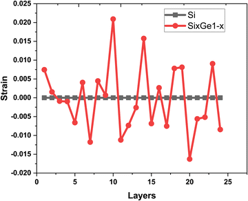 |
| | Fig. 9 The variation of strain extracted layer by layer in the Si thin film (shown by black square symbols and line) and SiGe thin film (shown by red dot symbols and line). | |
Conclusions
Si and SiGe epitaxy at the atomic scale is simulated through the chemical vapor deposition (CVD) process implemented in TNL-EpiGrow simulator. The optimum conditions to successfully reproduce the experimental output data in CVD growth are obtained by the design of experiments on the TNL-EpiGrow simulator. The inbuilt coupled algorithms in the TNL-EpiGrow simulator have shown capabilities to simultaneously handle the CVD reactor geometry-dependent chemical kinetics with the deposition processes. The output extraction capabilities provide a better understanding of the physical phenomenon inside the CVD chamber at the atomic scale. The proposed technique is found to be computationally efficient with potential to extract the thin film morphologies at the atomic scale, e.g., growth mode, point defects, strain layer by layer, growth in steps, surface roughness, and lattice parameters along with the chemical reaction kinetics data. The growth rates of Si using silane and disilane precursors and SiGe using silane and germane precursors have been successfully reproduced against the experimental findings. The observed growth modes justify S–K mode growth obtained during the experiments.
TNL-EpiGrow simulator can be used to develop a closed loop operation strategy to improve the thin film quality and to reduce the batch-to-batch variability caused by drift during the conditioning phase of CVD reactor operation. It is helpful for reactor design engineers associated with the development of CVD reactor processes associated with Si and SiGe deposition. The technique provides flexibility to optimize the chemical kinetics and growth conditions along with the flow rates of the precursors for getting optimum quality thin film wafers.
Author contributions
P. K. S. and P. S. developed the idea, theory and P. K. S. supervised the whole work. P. S developed the code, A. S., A. S. ran the simulations and did the data collection. P. K. S. written and edited the manuscript. All authors discussed the results and commented on the manuscript.
Availability of data
The data that support the findings of this study are available. All the results are produced from the TNL-EpiGrow simulator and are reproducible. Upon reasonable request to the corresponding author, he will provide access to the data associated with each result shown in the manuscript. The readers may directly download the TNL-EpiGrow simulator from https://www.technextlab.com to reproduce the data as an alternative option for the reproduction of the results reported here.
Conflicts of interest
The authors declare no competing interests. The authors declare that they have no known competing financial interests or personal relationships that could have appeared to influence the work reported in this paper.
References
- Ö. Danielsson, M. Karlsson, P. Sukkaew, H. Pedersen and L. Ojamäe, J. Phys. Chem. C, 2020, 124(14), 7725 CrossRef.
- D.-S. Byeon, C. Cho, D. Yoon, Y. Choi, K. Lee, S. Baik and D.-H. Ko, Coatings, 2021, 11, 568 CrossRef.
- O. Danielsson, U. Forsberg and E. Janz, J. Cryst. Grow., 2003, 250, 471 CrossRef.
- T. F. Kuech, Prog. Cryst. Growth Charact. Mater., 2016, 62, 352 CrossRef.
-
C. E. Morosanu, Thin Films by Chemical Vapour Deposition, Elsevier, New York, 1990 Search PubMed.
- C. C. Battaile and D. J. Srolovitz, Annu. Rev. Mater. Res., 2002, 32, 297 CrossRef.
-
H. O. Pierson, Handbook of Chemical Vapor Deposition (CVD) principles, technology, and applications, NOYES Publications, William Andrew Publishing, LLCNorwich, New York, USA, 1999 Search PubMed.
-
D. M. Dobkin, Principles of chemical vapor deposition, Kluwer Academic Publishers, 2003 Search PubMed.
- A. Santini and P. Politi, Am. J. Phys., 2018, 86(8), 616e621 CrossRef.
- in Thin Films: Heteroepitaxial Systems, (ed.) W. K. Liu and M. B. Santos, World Scientific, 1999 Search PubMed.
-
M. A. Herman, W. Richter and H. Sitter, Epitaxy: Physical Principles and Technical Implementation, Springer, Berlin, 2004 Search PubMed.
-
M. A. Herman and H. Sitter, Molecular Beam Epitaxy: Fundamentals and Current Status, Springer, Berlin, 2nd edn, 1996 Search PubMed.
- H. Ni, S. Lu and C. Chen Vivien, J. Cryst. Grow., 2014, 404, 89–99 CrossRef.
- V. Günther and F. Mauß, Phys. Proc., 2013, 40, 56–64 CrossRef.
- J. Pablo Balbuena and I. Martin-Bragado, Thin Solid Films, 2017, 634, 121–133 CrossRef.
-
B. Sklenard, A. Johnsson and A. La Magna, Review of experimental and model state of the art, 2020 ICT Project No 871813, MUNDFAB Modeling Unconventional Nanoscaled Device FABrication, 1-22. https://cordis.europa.eu/project/id/871813.
- P. K. Saxena, P. Srivastava and R. Trigunayat, J. Alloys Compd., 2019, 809, 151752 CrossRef.
- TNL-EpiGrowSimulator user manual, 2023, Tech Next Lab InC. https://www.technextlab.com/epi_g.html.
- P. K. Saxena, P. Srivastava and A. Srivastava, J. Cryst. Growth, 2024, 630, 127584 CrossRef.
-
A. Pimpinelli and J. Villain, Physics of Crystal Growth, Cambridge University Press, Cambridge, 1998 Search PubMed.
-
F. Much, PhD thesis, Bayerische Julius-Maximilians-Universitat Wurzburg, Wurzburg, 2003.
- M. Crose, J. Sang-Il Kwon, A. Tran and P. D. Christofides, Renewable Energy, 2017, 100, 129 CrossRef.
- R. Wang, R. Ma and M. Dudley, Ind. Eng. Chem. Res., 2009, 48, 3860 CrossRef.
- B. A. Scott and R. D. Estes, Appl. Phys. Lett., 1989, 55, 1005 CrossRef.
- R. L. Schwoebel and E. J. Shipsey, J. Appl. Phys., 1966, 37, 3682 CrossRef.
- G. Ehrlich and F. G. Hudda, J. Chem. Phys., 1966, 44, 1039 CrossRef.
- I. Kurganskaya, N. Khan Niazi and A. Luttge, J. Hazard. Mater., 2021, 417, 126005 CrossRef.
- T. N. Adam, S. Bedell, A. Reznicek, D. K. Sadana, A. Venkateshan, T. Tsunoda, T. Seino, J. Nakatsuru and S. R. Shinde, J. Cryst. Grow., 2010, 312, 3473 CrossRef.
-
B. Tillack and J. Murota, Silicon–germanium (SiGe) crystal growth using chemical vapor deposition, Woodhead Publishing Series in Electronic and Optical Materials, 2011, ch. 6, pp. 117–146 Search PubMed.
- N. Bartels, K. Golibrzuch, C. Bartels, L. Chen, D. J. Auerbach, A. M. Wodtke and T. Schäfer, Proc. Natl. Acad. Sci. U. S. A., 2013, 110(44), 17738–17743 CrossRef.
|
| This journal is © The Royal Society of Chemistry 2024 |
Click here to see how this site uses Cookies. View our privacy policy here. 
 Open Access Article
 This Open Access Article is licensed under a
  *,
P.
Srivastava
,
Anshika
Srivastava
and
Anshu
Saxena
*,
P.
Srivastava
,
Anshika
Srivastava
and
Anshu
Saxena


 and
and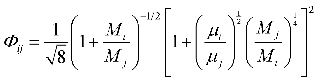
 . The total absorption (A) and hopping (H) rates are dependent on the sites available on the lattice. The rates of each type of event transitions (R) are calculated by eqn (2).
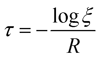
 with units in terms of mol, cm, s, cal, and K. Surface rate (ks) is in cm2 mol−1 s−1, gas rate (kg) is in cm3 mol−1 s−1.14 * and σ represent adsorbed species and free surface site, respectively