
 Open Access Article
 This Open Access Article is licensed under a
 Creative Commons Attribution 3.0 Unported Licence
In situ atomic-resolution study of transformations in double polymorph γ/β-Ga2O3 structures†
J.
García-Fernández
 *a,
S. B.
Kjeldby
a,
L. J.
Zeng
b,
A.
Azarov
a,
A.
Pokle
a,
P. D.
Nguyen
a,
E.
Olsson
b,
L.
Vines
a,
A.
Kuznetsov
*a and
Ø.
Prytz
*a
*a,
S. B.
Kjeldby
a,
L. J.
Zeng
b,
A.
Azarov
a,
A.
Pokle
a,
P. D.
Nguyen
a,
E.
Olsson
b,
L.
Vines
a,
A.
Kuznetsov
*a and
Ø.
Prytz
*a
aDepartment of Physics and Centre for Materials Science and Nanotechnology, University of Oslo, Oslo 0315, Norway. E-mail: j.g.fernandez@smn.uio.no; andrej.kuznetsov@fys.uio.no; oystein.prytz@fys.uio.no
bDepartment of Physics, Chalmers University of Technology, Gothenburg 41296, Sweden
First published on 11th March 2024
Abstract
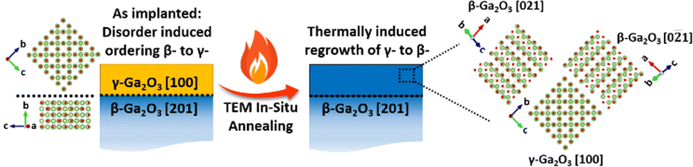
Disorder-induced formation of metastable Ga2O3 polymorphs as well as the recovery of the stable state upon annealing attract attention because of the fundamental novelty and rapidly increasing interest in the use of Ga2O3 in practical applications. In this study, double polymorph γ/β-Ga2O3 structures fabricated by the radiation-induced disorder approach were used as a starting point for systematic in situ annealing electron microscopy experiments. We show that, under the conditions of the TEM in situ annealing, double γ/β-Ga2O3 polymorph structures remained stable up to 300 °C, when onsets of the γ-to-β transformation become traceable, leading to a prominent γ- and β-mixture already at 500 °C. Interestingly, the recrystallization of the β-Ga2O3 occurs throughout the whole γ-film and the preferential alignments at the newly emerging γ/β-interfaces are different from that of the initial γ/β-interface formed as a result of the disorder-induced ordering. The alignments of the two polymorphs are maintained as a function of temperature – with a reduction in the volumetric ratio of γ-domains for increasing annealing temperature. Finally, at 1100 °C, γ-Ga2O3 fully transforms into β-Ga2O3, without dominating crystallographic relationships or preferred orientations, indicating that energy barriers are not any longer implied limiting factors, because of a sufficiently high thermal energy supply. Thus, these TEM in situ measurements enable a new level of accuracy for assessing polymorphic transformations in Ga2O3.
1. Introduction
Polymorphism contributes to the diversity of materials, so that even materials with the same chemical compositions exhibit variations in properties because of different crystal structures. Mechanistically, switching from one crystal structure to another depends on the ability of atoms to move out of their sites, which can be achieved by changing temperature and/or pressure.1 Moving atoms from their equilibrium positions by accelerated particle beams is another option; even though such polymorph transitions are rare due to a competing amorphization process. Nevertheless, disorder-induced formation of metastable polymorphs by irradiation has been observed in several materials,2–5 including gallium oxide (Ga2O3).6–13 At present, the mechanisms of polymorph transitions in Ga2O3 are under intensive investigation, because of the rapidly increasing interest in Ga2O3 for its use in power electronics and UV photonics.14–19 Indeed, since ion beam processing is often an inevitable part of the device fabrication, it is essential to establish full control over the polymorphism of Ga2O3, in particular upon ion implantation and annealing. Concurrently, there is a fundamental interest in studying reconstruction of the stable polymorph, since the rich polymorphism of Ga2O3 provides several potential reconstruction routes.The present understanding is that upon the introduction of the lattice disorder by ion implantation, the thermodynamically stable β-Ga2O3 (monoclinic, C2/m20,21) transforms into a metastable spinel γ-Ga2O3 (cubic, Fd![[3 with combining macron]](https://www.rsc.org/images/entities/char_0033_0304.gif) m20,21), forming a continuous and homogeneous γ-Ga2O3 layer on top of the β-Ga2O3 wafer; i.e. in the region containing the highest disorder induced by implanted ions and recoils.6–12 In the rest of the paper, we refer to this structure as a “double polymorph γ/β-Ga2O3 structure” and use it as a starting point for systematic in situ annealing experiments with an electron microscope, which is currently missing in the literature. Notably, until the disorder-induced β-to-γ transformation in Ga2O3 was explained,6–12 the interpretations of the annealing experiments of ion implanted β-Ga2O3 samples were carried out in terms of the reduction of the “radiation disorder” in an unchanged lattice – as is conventionally done for other materials. Thus, on top of the missing in situ studies, even ex situ annealing experiments of the ion implanted β-Ga2O3 – until very recently – neglected the aspect of the polymorph reconstruction. Moreover, even though the most recent ex situ studies revealed that γ-Ga2O3 eventually transforms back into thermodynamically stable β-Ga2O3 upon annealing,6,7,22–24 the kinetics of the process have not been clearly articulated. Indeed, apart from the transition temperature uncertainties, there are unresolved – and even previously unasked in literature – questions related e.g. to the nucleation sites of the “recrystallized” β-Ga2O3 as well as to its crystallographic alignment with the “initial” β-Ga2O3 matrix and eventually remaining γ-Ga2O3 inclusions. Another important question is whether the chemistry of the introduced ions affects the transformation upon annealing. The question is not trivial, since it has been shown that the γ-Ga2O3 formation as a result of the β-Ga2O3 disordering occurs independently of the chemical nature of the implanted ions,9,10 because of the prime role of the radiation-induced atomic displacements instead of the chemical effects, at least up to a certain impurity concentration.7,11,12 However, this may not necessarily hold for the transformations in double polymorph γ/β-Ga2O3 structures induced by temperature.
m20,21), forming a continuous and homogeneous γ-Ga2O3 layer on top of the β-Ga2O3 wafer; i.e. in the region containing the highest disorder induced by implanted ions and recoils.6–12 In the rest of the paper, we refer to this structure as a “double polymorph γ/β-Ga2O3 structure” and use it as a starting point for systematic in situ annealing experiments with an electron microscope, which is currently missing in the literature. Notably, until the disorder-induced β-to-γ transformation in Ga2O3 was explained,6–12 the interpretations of the annealing experiments of ion implanted β-Ga2O3 samples were carried out in terms of the reduction of the “radiation disorder” in an unchanged lattice – as is conventionally done for other materials. Thus, on top of the missing in situ studies, even ex situ annealing experiments of the ion implanted β-Ga2O3 – until very recently – neglected the aspect of the polymorph reconstruction. Moreover, even though the most recent ex situ studies revealed that γ-Ga2O3 eventually transforms back into thermodynamically stable β-Ga2O3 upon annealing,6,7,22–24 the kinetics of the process have not been clearly articulated. Indeed, apart from the transition temperature uncertainties, there are unresolved – and even previously unasked in literature – questions related e.g. to the nucleation sites of the “recrystallized” β-Ga2O3 as well as to its crystallographic alignment with the “initial” β-Ga2O3 matrix and eventually remaining γ-Ga2O3 inclusions. Another important question is whether the chemistry of the introduced ions affects the transformation upon annealing. The question is not trivial, since it has been shown that the γ-Ga2O3 formation as a result of the β-Ga2O3 disordering occurs independently of the chemical nature of the implanted ions,9,10 because of the prime role of the radiation-induced atomic displacements instead of the chemical effects, at least up to a certain impurity concentration.7,11,12 However, this may not necessarily hold for the transformations in double polymorph γ/β-Ga2O3 structures induced by temperature.
Thus, in the present work, we monitored structural transformations happening in double γ/β-Ga2O3 polymorph structures during annealing performed in situ with an electron microscope using samples fabricated with either Si or Au ion implants. Si implants were selected because of their technological relevance for n-type doping in Ga2O3,25 while Au implants were used for comparison, investigating possible chemical effects at the background of similar levels of the initial lattice disorder in both samples. We show that, under the conditions of the in situ electron microscope annealing, double γ/β-Ga2O3 polymorph structures remained stable up to 300 °C, when onsets of the γ-to-β transformation become traceable, leading to a prominent γ- and β-mixture already at 500 °C. Interestingly, the recrystallization of the β-Ga2O3 occurs throughout the whole γ-film and the preferential alignments of the newly emerging γ/β interfaces is different from that at the initial γ/β interface formed as a result of the disorder-induced ordering. This transformation pattern is maintained as a function of temperature – with a gradually reduced portion of the γ-domains. Finally, at 1100 °C, γ-Ga2O3 fully transforms into β-Ga2O3, without dominating crystallographic relationships or preferred orientations, indicating that energy barriers are not any longer implied as limiting factors because of the sufficiently high thermal energy supply. No apparent trends in the transformations were attributed to the chemical effects of the implanted species. The in situ TEM methodology enabled a new level of accuracy in the assessments of the transformations occurring in double polymorph γ/β-Ga2O3 structures.
2. Experimental section
Double γ/β-Ga2O3 polymorph structures used in this work were fabricated by implantation of the (010)-oriented β-Ga2O3 single crystal wafers with either 28Si+ or 197Au+. Specifically, 300 keV 28Si+ and 1.2 MeV 197Au+ ions were implanted with fluences of 2 × 10¹⁶ Si/cm2 and 3 × 10¹⁵ Au/cm2, respectively. The implants were performed at room temperature and at 7° from the surface normal to minimize possible channeling effects. The Si and Au implants result in 31 and 40 displacements per atom (dpa) in the maximum of the disorder peaks, respectively (see Fig. S1 and S2 in the ESI†). Similar implantation conditions were used previously in the literature for fabrication of double γ/β-Ga2O3 polymorph structures.9,10,22Subsequently, TEM lamellas were prepared by focused ion beam (FIB) using a JEOL JIB 4500 and a FEI Versa 3D DualBeam systems operating at 1–30 kV for the electron and Ga-ion beam. Final polishing of the TEM lamellas was done with a low ion beam energy (2 kV) and current (∼20 pA) to minimize the effect of the Ga-ion beam. The crystal wafers were first sputter-coated by carbon (∼20 nm) using a Leica EM ACE600 sputter system. Further ∼2 μm protective layers of C/W were deposited using an e-beam (eW), followed by a Ga-ion beam (iW). High-resolution scanning transmission electron microscopy (HRTEM/STEM) and selected area electron diffraction (SAED) were conducted using a Thermo Fisher Scientific Cs-corrected Titan G2 60–300![[thin space (1/6-em)]](https://www.rsc.org/images/entities/char_2009.gif) kV microscope operated at 300kV and equipped with a Gatan GIF Quantum 965 spectrometer. High angle annular dark field (HAADF) and bright field (BF) STEM images were recorded using a probe convergence semi-angle of 23 mrad, a nominal camera length of 60mm, corresponding to an inner and outer collection semi-angle of 100 and 200 mrad for HAADF and 0–22 mrad for BF, respectively. TEM in situ heating experiments (under vacuum) for the Si-implanted sample from RT to 850 °C in steps of 50 °C were done using a Gatan double tilt heating holder (model 652), keeping the sample at the target temperature for 30 minutes in each step. Additionally, we used a Protochips Fusion holder to repeat the same experiments for the Au implanted sample but with improved temperature control, stability, and a higher temperature range from RT to 1100 °C. As an example, Fig. S3 in the ESI† shows a low magnification BF STEM image of the prepared lamella. SAED patterns were acquired at each annealing temperature step during heating. Additional SAED patterns were acquired when cooling to RT to ensure that no crystal structure changes occurred during such cooling steps. All HAADF STEM images were recorded at RT. All the structural models for Ga2O3 polymorphs in this manuscript were displayed using VESTA software.26 In all lattice schematics used in the manuscript, gallium and oxygen atoms are represented in green and red, respectively. Higher color densities, darker green for gallium, are used for indicating higher atomic column density.
kV microscope operated at 300kV and equipped with a Gatan GIF Quantum 965 spectrometer. High angle annular dark field (HAADF) and bright field (BF) STEM images were recorded using a probe convergence semi-angle of 23 mrad, a nominal camera length of 60mm, corresponding to an inner and outer collection semi-angle of 100 and 200 mrad for HAADF and 0–22 mrad for BF, respectively. TEM in situ heating experiments (under vacuum) for the Si-implanted sample from RT to 850 °C in steps of 50 °C were done using a Gatan double tilt heating holder (model 652), keeping the sample at the target temperature for 30 minutes in each step. Additionally, we used a Protochips Fusion holder to repeat the same experiments for the Au implanted sample but with improved temperature control, stability, and a higher temperature range from RT to 1100 °C. As an example, Fig. S3 in the ESI† shows a low magnification BF STEM image of the prepared lamella. SAED patterns were acquired at each annealing temperature step during heating. Additional SAED patterns were acquired when cooling to RT to ensure that no crystal structure changes occurred during such cooling steps. All HAADF STEM images were recorded at RT. All the structural models for Ga2O3 polymorphs in this manuscript were displayed using VESTA software.26 In all lattice schematics used in the manuscript, gallium and oxygen atoms are represented in green and red, respectively. Higher color densities, darker green for gallium, are used for indicating higher atomic column density.
3. Results and discussion
3.1. As-fabricated double γ/β-Ga2O3 polymorph sample
Fig. 1 summarizes the TEM data collected from the as-fabricated samples. In particular Fig. 1(a) shows the low magnification BF STEM image and the corresponding SAED pattern of the Si-implanted sample, revealing a ∼380 nm thick γ-Ga2O3 layer formed as a consequence of the radiation-induced disorder. The γ-Ga2O3 layer formed as a result of Au-implants looks similar, see Fig. S3 in the ESI,† as expected because of the similar radiation disorder produced by both ions (see the explanation for the disorder calculations in the ESI†). This is in accordance with previous literature reports concerning the disorder-induced β- to γ-polymorph transition.6–12 Notably, the newly formed γ-Ga2O3 is aligned with respect to the original β-Ga2O3 substrate following the crystallographic relationship: [100] γ-Ga2O3//[201] β-Ga2O3 and [110] γ-Ga2O3//[132] β-Ga2O3. This crystallographic orientation is probably due to the in-plane matching (for planes vertical to the interface) between the newly formed γ-Ga2O3 and original β-Ga2O3.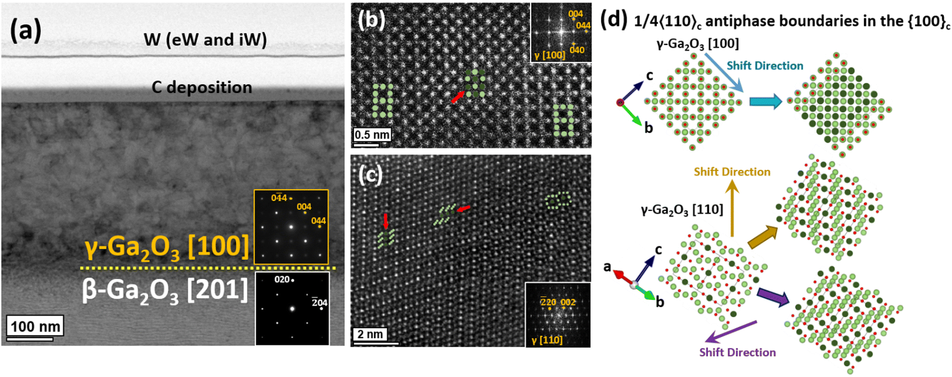 | ||
| Fig. 1 Microscopy analysis of as-implanted samples. (a) Low magnification BF STEM image and SAED patterns of the Si-implanted sample showing the formation of the double γ/β-Ga2O3 polymorph structure. (b) HAADF STEM image and corresponding FFT of γ-Ga2O3 along the [100] zone axis for the Si-implanted sample. (c) HAADF STEM image and corresponding FFT of γ-Ga2O3 along the [110] zone axis for the Au-implanted sample. (d) Schematic representation of the lattices of γ-Ga2O3 along [100] and [110] zone axes, together with the projected model structures and the lattice shifts as a consequence of the APB. Color code: Ga green (dark green represents high density occupancy sites), O red. | ||
There is a stacking similarity between the interplanar distances d(044) = 1.48 Å and d(−111) = 4.83 Å of γ-Ga2O3 with d(−204) = 1.47 Å and d(−201) = 4.82 Å of β-Ga2O3 phases, respectively. Furthermore, Fig. 1(b) and (c) show HAADF STEM images and corresponding fast Fourier transforms (FFT) of γ-Ga2O3 along the [100] zone axis for the Si-implanted sample, and along the [110] zone axis for the Au-implanted sample. Both images show the presence of antiphase boundaries (APB), indicated by red arrows, that are characterized by the displacement vector 1/4〈110〉c in the {100}c planes of the cubic spinel structure. Consequently, Fig. 1(d) shows two schematic representations of the γ-Ga2O3 lattice (viewed along the [100] and [110] directions) including the formation of APBs as a result of the atomic shifts. These schematics are in good agreement with the contrast observed in the HAADF STEM images in Fig. 1(b) and (c). Similar APBs in the γ-Ga2O3 spinel structure have been reported in the literature.8,27–29 Thus, in the initial stage, the samples used in this study are representative examples of the double γ/β-Ga2O3 polymorph structures. No apparent differences were detected in the quality of the γ-Ga2O3 produced either by Si or Au implants. We used both samples in the in situ study to check for possible differences at the annealing stage.
3.2. In situ monitoring of the γ- to β-polymorph transition
Fig. 2(a)–(d) display the evolution in the SAED patterns for the Si-implanted sample, at RT and after in situ annealing at 500 °C, 700 °C, and 850 °C, respectively. The γ-Ga2O3 layer was initially tilted to the [100] zone axis at RT, as shown in the indexed SAED pattern in Fig. 2(a). Notably, each SAED pattern is accompanied by an inset showing the scaled features around the (022) spot of the γ-Ga2O3 to highlight the structural changes. We observed an onset γ- to β-polymorph transition already at ∼300 °C (not observed at 250 °C, see Fig. S4 in the ESI†) and prominently occurring at 500 °C. The formation of the β-phase in the γ-Ga2O3 layer is confirmed by the emergence of new diffraction spots in the SAED pattern in Fig. 2(b). These new spots can be indexed as β-Ga2O3 phase domains (represented by red and blue colors) along the [021] and [0![[2 with combining macron]](https://www.rsc.org/images/entities/char_0032_0304.gif) 1] zone axes, which are related by a 90° rotation. This could be induced by the four-fold symmetry of γ-Ga2O3 along the [100] direction, which may direct the formation of β-domains with a 90° rotational relationship. Subsequently, upon reaching 700 °C, weaker spots surrounding the (022) spot become visible, as indicated by green dashed circles in the inset in Fig. 2(c). The number of these spots increases upon reaching 850 °C, see the inset in Fig. 2(d). Additionally, the transformation from γ- to β-Ga2O3 is confirmed by EELS spectra in Fig. S5 in the ESI.† Fig. S5 (ESI†) shows the evolution of the O–K edge for the as-implanted γ-Ga2O3 and after annealing at 500 °C and 850 °C, together with bulk β-Ga2O3, as a reference. The O K-edge is characterized by two peaks at 537 eV and 543 eV,10,24 and the relative intensity between these peaks can be used as a fingerprint of the corresponding polymorph. Importantly, we did not observe any change in the sample while cooling the samples to room temperature, confirming the stability of the transformation, and enabling accurate high-resolution measurements.
1] zone axes, which are related by a 90° rotation. This could be induced by the four-fold symmetry of γ-Ga2O3 along the [100] direction, which may direct the formation of β-domains with a 90° rotational relationship. Subsequently, upon reaching 700 °C, weaker spots surrounding the (022) spot become visible, as indicated by green dashed circles in the inset in Fig. 2(c). The number of these spots increases upon reaching 850 °C, see the inset in Fig. 2(d). Additionally, the transformation from γ- to β-Ga2O3 is confirmed by EELS spectra in Fig. S5 in the ESI.† Fig. S5 (ESI†) shows the evolution of the O–K edge for the as-implanted γ-Ga2O3 and after annealing at 500 °C and 850 °C, together with bulk β-Ga2O3, as a reference. The O K-edge is characterized by two peaks at 537 eV and 543 eV,10,24 and the relative intensity between these peaks can be used as a fingerprint of the corresponding polymorph. Importantly, we did not observe any change in the sample while cooling the samples to room temperature, confirming the stability of the transformation, and enabling accurate high-resolution measurements.
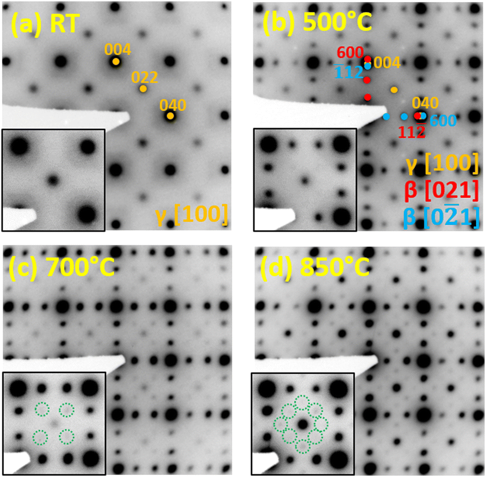 | ||
| Fig. 2 Comparison of the SAED patterns from the Si-implanted sample in (a) the as-fabricated state, with that upon in situ annealing at (b) 500 °C, (c) 700 °C, and (d) 850 °C. The insets show the scaled-up features around the (022) spot. Color code: orange: γ-Ga2O3 along the [100] zone axis, red and blue: β-Ga2O3 along the [021] and [01] zone axes, respectively. | ||
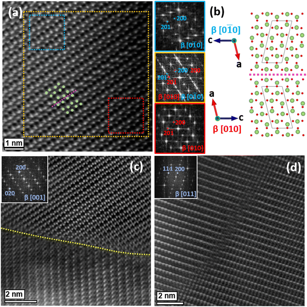
Indeed, Fig. 3 provides an example of such atomic-resolution measurements for samples annealed at 500 °C and 850 °C. Specifically, Fig. 3(a) and (b) depict low and high magnification HAADF STEM images of the Si-implanted sample after heating at 500 °C. In both images, two types of β-Ga2O3 domains can be observed, oriented along the [021] and [01] directions and related to each other by a 90° rotation, marked in blue and red. Importantly, Fig. 3(b) is accompanied by two extra panels, showing the FFTs obtained from the areas marked by red and blue dashed rectangles. These FFTs confirm the presence of remaining γ-Ga2O3 in the [100] orientation and reveal the presence of individual β-Ga2O3 domains exhibiting the [021]/[01] orientations with a 90° rotational relationship as described above. Fig. 3(c) displays a HAADF STEM image of the sample after heating at 850 °C. On the left-hand side in Fig. 3(c), the remaining γ-Ga2O3 is still visible, together with the presence of APBs, identified already in the as-fabricated samples. On the right-hand side of Fig. 3(c), the contrast associated with β-Ga2O3 along the [021] zone axis is clearly observed. Additionally, the presence of APBs between two β-phase regions is visible in Fig. 3(c), as indicated by the red arrow. Thus, Fig. 3(c), in combination with the SAED pattern (Fig. 2(d)), confirms the presence of remaining γ-Ga2O3 upon 850 °C annealing. For clarity, Fig. 3(d) provides a detailed view of the interface between the [100] γ-Ga2O3 (left) and [021] β-Ga2O3 (right) phases, taken from the region marked with a green rectangle in Fig. 3(c), accompanied by schematic representations of both phases. As can be deduced from Fig. 3(d), the γ- to β-polymorph transition proceeds via the stacking of {400} γ-Ga2O3 to {600} β-Ga2O3 planes. We suggest that the newly formed strong spots observed in Fig. 2(b)–(d) correspond to the formation of new β-phase along the [021] direction, while the weaker spots marked with dashed green in Fig. 2(c) and (d) could be a consequence of the presence of domains and extended defects resulting from the recrystallization of the β-Ga2O3 phase, consistently with the literature.30–32 Recently, the presence of four rotational domains of β-Ga2O3 related by a 90° rotation has been reported for β-Ga2O3 grown on top of γ-Ga2O3.33 Thus, in our samples, cubic γ-Ga2O3 may play a similar role, promoting the domains formation.
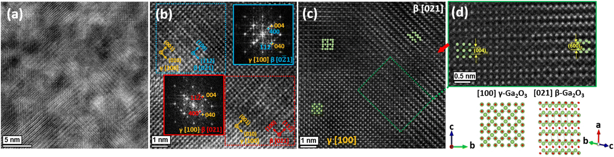 | ||
| Fig. 3 Atomic-resolution measurements of the Si-implanted sample upon annealing at 500 °C and 850 °C. (a) Low and (b) high magnification HAADF STEM images and corresponding FFTs of the Si-implanted sample after heating at 500 °C. (c) Atomic resolution HAADF STEM images of the same sample after heating at 850 °C showing the presence of [100] γ-Ga2O3 (left) and [021] β-Ga2O3 (right) with the presence of extensive defects such as APBs (red arrow). (d) HAADF STEM image at the interface between the two polymorphs. Schematic representation of [100] γ-Ga2O3 and [021] β-Ga2O3 polymorphs. Color code: Ga green (dark green represents high density occupancy sites), O red. | ||
To control the generic character of the γ- to β-polymorph transition observed in Fig. 2 and 3, we repeated the experiment with the Au-implanted sample. This also allows us to explore the different crystallographic orientation between γ-Ga2O3 and the newly formed β-Ga2O3. Firstly, Fig. S4 in the ESI† shows an HRTEM image and corresponding FFT from different areas after annealing at 300 °C. Upon careful inspection in some of the FFTs, we observe the formation of additional weak spots assigned to β-Ga2O3 inclusions, confirming the γ- to β-polymorph transition starts already ∼300 °C (these inclusions were not observed at 250 °C). Furthermore, Fig. 4(a)–(c) display the SAED patterns of the Au-implanted sample acquired at RT as well as after heating at 500 °C and 700 °C. The SAED pattern acquired at RT can be indexed to the γ-Ga2O3 phase along the [110] zone axis (see the orange indexing in Fig. 4(a)). After heating, additional spots emerge in the SAED pattern marked by red and blue spots in Fig. 4(b). Similar to the Si-implanted sample, these new spots can be indexed as two separate β-Ga2O3 domains, in this case, oriented along the [010] and [0![[1 with combining macron]](https://www.rsc.org/images/entities/char_0031_0304.gif) 0] zone axes. This observation is in full agreement and correlation with the data obtained for the Si-implanted sample acquired from a different zone axis. This is because the angle between [100] and [110] directions in the γ-phase (45°) is similar to that for [021] and [010] directions in the β-phase (43.68°). As shown in the SAED pattern, like in the previous case, there is perfect overlapping between the (004) plane of γ-Ga2O3 with the (600) plane of β-Ga2O3. The HAADF STEM image recorded after heating at 500 °C (Fig. 4(d)) displays the remaining γ-Ga2O3 phase, as well as the newly formed [010] β-Ga2O3 domains in the presence of the stacking faults which have been observed previously in the literature.34 The green and blue squares in Fig. 4(d) show details of the defect associated with the newly formed β-Ga2O3 phase. Finally, Fig. 4(e) shows a representative HAADF STEM image and corresponding FFTs taken at the interface, indicated by a dashed yellow line, between the newly formed β-phase along the [010] zone axis and the original (untransformed) β-phase along the [132] zone axis after heating at 700 °C, confirming that the crystallographic relationship between γ-Ga2O3 and the original β-Ga2O3 is different from the crystallographic relationship between γ-Ga2O3 and the recrystallized β-Ga2O3. Thus, taking into account data in Fig. 2–4, we conclude that the γ- to β-polymorph transition in the double γ/β-polymorph structure fabricated via Si and Au ion implantation occurs in a generic and analogous manner, at least for the dose range and in situ TEM annealing conditions (under vacuum) used in our experiment.
0] zone axes. This observation is in full agreement and correlation with the data obtained for the Si-implanted sample acquired from a different zone axis. This is because the angle between [100] and [110] directions in the γ-phase (45°) is similar to that for [021] and [010] directions in the β-phase (43.68°). As shown in the SAED pattern, like in the previous case, there is perfect overlapping between the (004) plane of γ-Ga2O3 with the (600) plane of β-Ga2O3. The HAADF STEM image recorded after heating at 500 °C (Fig. 4(d)) displays the remaining γ-Ga2O3 phase, as well as the newly formed [010] β-Ga2O3 domains in the presence of the stacking faults which have been observed previously in the literature.34 The green and blue squares in Fig. 4(d) show details of the defect associated with the newly formed β-Ga2O3 phase. Finally, Fig. 4(e) shows a representative HAADF STEM image and corresponding FFTs taken at the interface, indicated by a dashed yellow line, between the newly formed β-phase along the [010] zone axis and the original (untransformed) β-phase along the [132] zone axis after heating at 700 °C, confirming that the crystallographic relationship between γ-Ga2O3 and the original β-Ga2O3 is different from the crystallographic relationship between γ-Ga2O3 and the recrystallized β-Ga2O3. Thus, taking into account data in Fig. 2–4, we conclude that the γ- to β-polymorph transition in the double γ/β-polymorph structure fabricated via Si and Au ion implantation occurs in a generic and analogous manner, at least for the dose range and in situ TEM annealing conditions (under vacuum) used in our experiment.
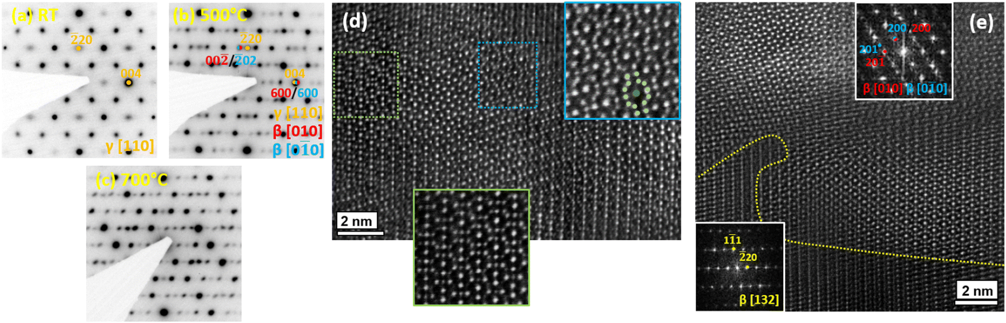 | ||
| Fig. 4 Complementary microscopy data measured on the Au-implanted sample. SAED patterns for (a) as-fabricated state, with that upon in situ annealing at (b) 500 °C and (c) 700 °C. Color code: orange: γ-Ga2O3 along the [110] zone axis, red and blue: β-Ga2O3 along the [010] and [00] zone axes. (d) and (e) HAADF STEM images and corresponding FFT after heating at 500 °C and 700 °C, respectively. The green and blue boxes in figure (d) correspond to two domains of the [010] β-phase. Color code: Ga green (dark green represents high density occupancy sites). The dashed yellow line in figure (e) indicates the interface between the original (untransformed) β-Ga2O3 and the newly formed β-Ga2O3. | ||
Furthermore, to investigate whether the β-matrix could be recovered with high temperature annealing, we performed in situ heating of the Au-implanted sample up to 1100 °C. Notably, after annealing at 1100 °C, the γ-Ga2O3 has been completely transformed to β-Ga2O3 in other orientations. For example, Fig. 5(a) shows an area of the TEM lamella containing newly formed β-Ga2O3 viewed along the [010] direction. In addition, the corresponding FFT of two domains (blue and red) and the global FFT from the region marked in orange are included as insets. The FFTs obtained from the blue and red areas confirm the presence of two domains of [010] and [00] β-Ga2O3 separated by a twin boundary indicated by the pink dashed line. For clarity, Fig. 5(b) displays a schematic representation of [010] β-Ga2O3 resulting in the twin boundary observed in Fig. 5(a). Similar results were previously observed in β-Ga2O3 domains related by a twin boundary in the literature.31,35,36
 | ||
| Fig. 5 HAADF STEM images of the Au-implanted sample after heating at 1100 °C. (a) β-Ga2O3 along the [010] direction with corresponding global FFT (orange) and local FFT taken from different areas (red and blue boxes) corresponding to two different domains. (b) Schematic representation of both domains and the twin boundary indicated by the pink dashed line. Ga atomic columns are represented in green and O in red. (c) Image recorded at the interface (indicated by a dashed yellow line) between newly formed [010] β-Ga2O3 and original (untransformed) [132] β-Ga2O3. (d) Image recorded from another area of the lamella corresponding to newly formed [011] β-Ga2O3 containing APB. | ||
Nevertheless, we found that the crystallographic relationship deduced from the SAED patterns in Fig. 4(b) and (c) was no longer maintained. Fig. 5(c) shows a HAADF STEM image of the interface between the original and the newly formed β-Ga2O3, with the interface marked by the dashed yellow line. Here, the original (untransformed) β-Ga2O3 is viewed along the [132] zone axis, while the newly formed β-Ga2O3 is now viewed along the [001] zone axis instead. Additionally, Fig. 5(d) displays a HAADF STEM image of the newly formed β-phase from another area of the lamella at the same tilting angle, oriented in the [011] direction, and revealing the presence of an APB. In both cases, this crystallographic relationship is different from that initially observed for lower annealing temperatures, as in Fig. 4(e) at 700 °C.
3.3. Discussion
The data in Fig. 1–5 provide new insights on how the metastable γ-Ga2O3, formed by the disorder-induced transformation, converts back into β-Ga2O3 upon annealing. In our interpretation, under the annealing conditions used in this work, β-Ga2O3 forms domains exhibiting the crystallographic relationship of [021] β-Ga2O3//[100] γ-Ga2O3 and [010] β-Ga2O3//[110] γ-Ga2O3. Importantly, looking accurately into the SAED patterns, e.g. in Fig. 2(b) and 3(b), we observe that some of the interplanar distances in the γ- and β-polymorphs are rather similar. Specifically, we see that the lattice spacing of 2.06 Å for (400) planes in the γ-Ga2O3 is close to that of 1.98 Å and 2.10 Å for (600) and (11) planes in the β-Ga2O3, respectively. Such similarity in distances may contribute to the reduction of the strain barrier associated with the recrystallization of the β-Ga2O3 domains inside the γ-film. Our results also showed that the nucleation of β-Ga2O3 domains takes place all over the γ-layer, and not in a preferential location, such as at the γ/β-interface. Spectacularly, these newly formed β-Ga2O3 domains exhibit different preferential crystallographic stacking with the γ-lattice as compared to that in the initial γ/β-interface. Recent reports37,38 suggest the existence of similarities between the two polymorphs: (i) both phases exhibit a face-centered cubic oxygen lattice, and (ii) the similarity in the cations positions (similar Ga sites in both lattices and Ga sites of the γ-phase that correspond to Ga interstitial sites in the β-phase). Considering this, the γ-phase was described as a disordered version of the β-phase, where cations from regular sites on the β-lattice are displaced to interstitial sites, leaving a vacancy. Therefore, this phase transition can be considered as a disorder–order transition induced by temperature. For clarity, Fig. 6 illustrates the dominating orientation relationships observed in our samples.
 | ||
| Fig. 6 Schematics of the dominating orientation relationships observed in our samples. | ||
Notably, the formation of β-Ga2O3 domains inside the γ-matrix upon ex situ annealing was proposed in the literature too, specifically suggesting that the defects available in the γ-matrix may induce the formation of such β-domains at temperatures below those require for a massive γ-to-β transition.23 This hypothesis is in agreement with our data, where high concentrations of APBs in the γ-Ga2O3 triggers the formation of β-Ga2O3 already at 300 °C. Further on, for the annealing in the range of 900–1100 °C, the remaining γ-Ga2O3 back-transforms to β-Ga2O3 without preferential orientations, indicating that energy barriers are no longer implied as limiting factors because of a high enough thermal energy supplied.
Importantly, the parameters controlling the polymorphism in a macroscopic sample (typically used in the ex situ annealing experiments in the literature8,22) and in a TEM-lamella sized sample (as used in this work) – may be different. Consequently, there could be potential discrepancies between the in situ and ex situ observations. In this sense, J. Wang et al.39 showed experimentally and by first-principles calculations that similar transitions occur in Ga2O3 nanowires. From their results, the calculated surface energy of {600}β is smaller than that of {400}γ. Considering that a TEM-lamella has a higher surface area/volume ratio than a bulk sample, the observed transition in this work could be influenced by the reduction of the surface energy. Moreover, all in situ annealing in the electron microscope was performed in high vacuum, featuring quite different conditions as compared to that in air or gas flow frequently used in the literature for ex situ annealing. In its turn, it is well-known that the differentiation between the oxygen rich or lean conditions may radically change properties of oxides.40 Thus, this factor might be considered while comparing in situ and ex situ observations too. For example, in our previous study of ex situ air annealing of the double polymorph γ/β-Ga2O3 structure fabricated using similar Si ion implantation conditions,22 the subsequent crystallographic relationship between the two phases was different. Moreover, in the present work, we have not detected precipitations correlated with the implants, e.g. in the form of SiOx nanoparticles nor voids, which were also observed during air annealing in our previous work.22 All-in-all, the results in Fig. 1–5, taken in the context of the literature data, confirm the complexity of the processes occurring in the double polymorph γ/β-Ga2O3 structures upon annealing.
4. Conclusions
In conclusion, we performed in situ TEM annealing studies of the double γ/β-Ga2O3 polymorph structures fabricated by the radiation induced disorder approach and revealed several new interesting trends for the γ-to-β polymorph transition. The in situ TEM study reveals the emergence of β-Ga2O3 domains at temperatures around 300 °C. The nucleation of these newly formed β-Ga2O3 domains take place according to the crystallographic relationship: [100] γ-Ga2O3//[021] β-Ga2O3 and [110] γ-Ga2O3//[010] β-Ga2O3, possibly explicable by the reduction of the surface energy and strain minimization due to very similar lattice plane spacings in the polymorphs. This was interpreted in terms of the reduction of the strain barrier associated with the formation of the β-Ga2O3 domains inside the γ-film. Importantly, these orientations are different from that established at the initial as-implanted γ/β-interface. However, at high temperatures (900–1100 °C), γ-Ga2O3 fully recrystallizes into β-Ga2O3 in other orientations, indicating that energy barriers are not any longer implied as limiting factors because of a sufficiently high thermal energy supply. Thus, the in situ observation methodology enabled a novel unprecedented accuracy in the assessments of the γ-to-β polymorph transition.Author contributions
J. G. F. and S. B. K.: conceptualization, data curation, formal analysis, investigation, methodology, visualization, writing original draft, writing – review and editing. L. J. Z., A. A., A. P., P. D. N.: formal analysis, investigation, methodology, visualization, writing original draft, writing – review and editing. E. O., L. V., A. K. and Ø. P.: formal analysis, funding acquisition, investigation, project administration, resources, supervision, validation, writing – review & editing.Conflicts of interest
There are no conflicts to declare.Acknowledgements
The Research Council of Norway is acknowledged for support through the projects NANO2021 researcher project Functionalization of conducting oxides by ion beam and defect engineering (FUNCTION, no. 287729) and the M-ERA.NET Program via GOFIB project (no. 337627). We also acknowledge the Norwegian Center for Transmission Electron Microscopy (NORTEM, no. 197405/F50), the Norwegian Micro- and Nanofabrication Facility (NorFab, no. 295864), and NordForsk is acknowledged for support to the NordTEMhub project no. 96971. Viktor Mihaly Bobal is acknowledged for performing ion implantation on the samples studied herein. This work was performed in part at the Chalmers Material Analysis Laboratory, CMAL. The authors acknowledge the financial support from Swedish Research Council (VR) and Swedish Foundation for Strategic Research (SSF) for the access to ARTEMI, the Swedish National Infrastructure in Advanced Electron Microscopy (2021-00171 and RIF21-0026).References
- W. Li, X. Qian and J. Li, Nat. Rev. Mater., 2021, 6, 829 CrossRef CAS.
- M. Ishimaru, I. V. Afanasyev-Charkin and K. E. Sickafus, Appl. Phys. Lett., 2000, 76, 2556 CrossRef CAS.
- S. Dhara, A. Datta, C. T. Wu, Z. H. Lan, K. H. Chen, Y. L. Wang, C. W. Hsu, C. H. Shen, L. C. Chen and C. C. Chen, Appl. Phys. Lett., 2004, 84, 5473 CrossRef CAS.
- A. Benyagoub, Phys. Rev. B: Condens. Matter Mater. Phys., 2005, 72, 094114 CrossRef.
- G. Sattonnay and L. Thomé, J. Nucl. Mater., 2006, 348, 223 CrossRef CAS.
- K. R. Gann, N. Pieczulewski, C. A. Gorsak, K. Heinselman, T. J. Asel, B. A. Noesges, K. T. Smith, D. M. Dryden, H. G. Xing, H. P. Nair, D. A. Muller and M. O. Thompson, J. Appl. Phys., 2024, 135, 015302 CrossRef CAS.
- H.-L. Huang, C. Chae, J. M. Johnson, A. Senckowski, S. Sharma, U. Singisetti, M. H. Wong and J. Hwang, APL Mater., 2023, 11, 061113 CrossRef CAS.
- T. Yoo, X. Xia, F. Ren, A. Jacobs, M. J. Tadjer, S. Pearton and H. Kim, Appl. Phys. Lett., 2022, 121, 072111 CrossRef CAS.
- J. García-Fernández, S. B. Kjeldby, P. D. Nguyen, O. B. Karlsen, L. Vines and Ø. Prytz, Appl. Phys. Lett., 2022, 121, 191601 CrossRef.
- A. Azarov, J. G. Fernández, J. Zhao, F. Djurabekova, H. He, R. He, Ø. Prytz, L. Vines, U. Bektas, P. Chekhonin, N. Klingner, G. Hlawacek and A. Kuznetsov, Nat. Commun., 2023, 14, 4855 CrossRef CAS PubMed.
- H.-L. Huang, J. M. Johnson, C. Chae, A. Senckowski, M. H. Wong and J. Hwang, Appl. Phys. Lett., 2023, 122, 251602 CrossRef CAS.
- J. Zhao, J. G. Fernández, A. Azarov, R. He, Ø. Prytz, K. Nordlund, M. Hua, F. Djurabekova and A. Kuznetsov, arXiv, 2024, preprint, arXiv:2401.07675 DOI:10.48550/arXiv.2401.07675.
- A. Azarov, C. Bazioti, V. Venkatachalapathy, P. Vajeeston, E. Monakhov and A. Kuznetsov, Phys. Rev. Lett., 2022, 128, 015704 CrossRef CAS PubMed.
- S. J. Pearton, F. Ren, M. Tadjer and J. Kim, J. Appl. Phys., 2018, 124, 220901 CrossRef.
- M. J. Tadjer, Science, 2022, 378, 724 CrossRef CAS PubMed.
- J. Xu, W. Zheng and F. Huang, J. Mater. Chem. C, 2019, 7, 8753 RSC.
- W. Choi, D.-W. Jeon, J.-H. Park, D. Lee, S. Lee, K. H. Baik and J. Kim, Mater. Adv., 2023, 4, 4520 RSC.
- B. Zhao, F. Wang, H. Chen, L. Zheng, L. Su, D. Zhao and X. Fang, Adv. Funct. Mater., 2017, 27, 1700264 CrossRef.
- D. Zhang, H. Yu, G. You, G. Shao, Z. Fang, Z. Liang, T. Zhang, H. Hou, L. Wang, Q. Chen, J. Teng and W. Yang, J. Mater. Sci. Technol., 2023, 163, 150 CrossRef CAS.
- M. Bosi, P. Mazzolini, L. Seravalli and R. Fornari, J. Mater. Chem. C, 2020, 8, 10975 RSC.
- H. Y. Playford, A. C. Hannon, E. R. Barney and R. I. Walton, Chem. – Eur. J., 2013, 19, 2803 CrossRef CAS PubMed.
- S. B. Kjeldby, A. Azarov, P. D. Nguyen, V. Venkatachalapathy, R. Mikšová, A. Macková, A. Kuznetsov, Ø. Prytz and L. Vines, J. Appl. Phys., 2022, 131, 125701 CrossRef CAS.
- P. Castro-Fernández, M. V. Blanco, R. Verel, E. Willinger, A. Fedorov, P. M. Abdala and C. R. Müller, J. Phys. Chem. C, 2020, 124, 20578 CrossRef.
- A. Sharma, M. Varshney, H.-J. Shin, K. H. Chae and S. O. Won, RSC Adv., 2017, 7, 52543 RSC.
- A. T. Neal, S. Mou, S. Rafique, H. Zhao, E. Ahmadi, J. S. Speck, K. T. Stevens, J. D. Blevins, D. B. Thomson, N. Moser, K. D. Chabak and G. H. Jessen, Appl. Phys. Lett., 2018, 113, 062101 CrossRef.
- K. Momma and F. Izumi, J. Appl. Crystallogr., 2011, 44, 1272 CrossRef CAS.
- M. Mitome, S. Kohiki, T. Nagai, K. Kurashima, K. Kimoto and Y. Bando, Cryst. Growth Des., 2013, 13, 3577 CrossRef CAS.
- C. S. Chang, N. Tanen, V. Protasenko, T. J. Asel, S. Mou, H. G. Xing, D. Jena and D. A. Muller, APL Mater., 2021, 9, 051119 CrossRef CAS.
- J. Tang, K. Jiang, S. D. House, C. Xu, K. Xiao, L. M. Porter and R. F. Davis, Appl. Phys. Lett., 2023, 123, 012103 CrossRef CAS.
- P. Mazzolini, A. Falkenstein, C. Wouters, R. Schewski, T. Markurt, Z. Galazka, M. Martin, M. Albrecht and O. Bierwagen, APL Mater., 2020, 8, 011107 CrossRef CAS.
- G. Wagner, M. Baldini, D. Gogova, M. Schmidbauer, R. Schewski, M. Albrecht, Z. Galazka, D. Klimm and R. Fornari, Phys. Status Solidi A, 2014, 211, 27 CrossRef CAS.
- S. Gao, Y. Wu, R. Kang and H. Huang, Mater. Sci. Semicond. Process., 2018, 79, 165 CrossRef CAS.
- K. Jiang, J. Tang, C. Xu, K. Xiao, R. F. Davis and L. M. Porter, J. Vac. Sci. Technol., A, 2023, 41, 062702 CrossRef CAS.
- D. Gogova, G. Wagner, M. Baldini, M. Schmidbauer, K. Irmscher, R. Schewski, Z. Galazka, M. Albrecht and R. Fornari, J. Cryst. Growth, 2014, 401, 665 CrossRef CAS.
- R. Schewski, K. Lion, A. Fiedler, C. Wouters, A. Popp, S. V. Levchenko, T. Schulz, M. Schmidbauer, S. Bin Anooz, R. Grüneberg, Z. Galazka, G. Wagner, K. Irmscher, M. Scheffler, C. Draxl and M. Albrecht, APL Mater., 2019, 7, 022515 CrossRef.
- S. Vura, U. Ul Muazzam, V. Kumar, S. C. Vanjari, R. Muralidharan, N. Digbijoy, P. Nukala and S. Raghavan, ACS Appl. Electron. Mater., 2022, 4, 1619 CrossRef CAS.
- C. Wouters, M. Nofal, P. Mazzolini, J. Zhang, T. Remmele, A. Kwasniewski, O. Bierwagen and M. Albrecht, APL Mater., 2024, 12, 011110 CrossRef CAS.
- J. Tang, K. Jiang, C. Xu, M. J. Cabral, K. Xiao, L. M. Porter and R. F. Davis, APL Mater., 2024, 12, 011109 CrossRef CAS.
- J. Wang, X. Guan, H. Zheng, L. Zhao, R. Jiang, P. Zhao, Y. Zhang, J. Hu, P. Li, S. Jia and J. Wang, Nano Lett., 2023, 23, 7364 CrossRef CAS PubMed.
- T. M. Børseth, B. G. Svensson, A. Y. Kuznetsov, P. Klason, Q. X. Zhao and M. Willander, Appl. Phys. Lett., 2006, 89, 262112 CrossRef.
Footnote |
| † Electronic supplementary information (ESI) available. See DOI: https://doi.org/10.1039/d3ma01011b |
| This journal is © The Royal Society of Chemistry 2024 |