
 Open Access Article
 This Open Access Article is licensed under a
 Creative Commons Attribution 3.0 Unported Licence
Realization of giant superstructural chirality at broadband optical wavelengths via perovskite dielectric metasurfaces†
Aqsa
Asad‡
a,
Hafiz Saad
Khaliq‡
 a,
Min-Seok
Kim
a,
Jae-Won
Lee
a and
Hak-Rin
Kim
*ab
a,
Min-Seok
Kim
a,
Jae-Won
Lee
a and
Hak-Rin
Kim
*ab
aSchool of Electronic and Electrical Engineering, Kyungpook National University, Daegu 41566, Republic of Korea
bSchool of Electronics Engineering, Kyungpook National University, Daegu 41566, Republic of Korea. E-mail: rineey@knu.ac.kr
First published on 31st January 2024
Abstract
Recently, perovskite materials have gained much attention for their potential in large chirality applications, particularly in chiral photonics and metamaterials. However, the intended chirality response is not achieved due to the substantial size disparity and the limited interactions between the structures and the wavelength of light. To overcome these limitations, we propose a planar all-dielectric nanostructure-based metasurface integrated with perovskite to realize exceptional superstructural chirality in the broadband visible regime. A low-loss dielectric hydrogenated amorphous silicon (a-Si:H) and the perovskite cesium lead bromide (CsPbBr3) are used to design this giant superstructural chiral perovskite metasurface. Due to the strong interaction of light with the proposed chiral perovskite metasurface and tuning of the electric and magnetic multipolar resonances, it achieved the maximum anisotropy factor of ∼1.55 and the circular dichroism of ∼42![[thin space (1/6-em)]](https://www.rsc.org/images/entities/char_2009.gif) 934 (mdeg), almost reaching the theoretical limit of 2.0 and 45000 (mdeg), respectively. This perovskite integration with dielectric chiral metasurfaces could pave the way for potential applications in chiral photonics, spintronics, and optoelectronics.
934 (mdeg), almost reaching the theoretical limit of 2.0 and 45000 (mdeg), respectively. This perovskite integration with dielectric chiral metasurfaces could pave the way for potential applications in chiral photonics, spintronics, and optoelectronics.
1. Introduction
In the realm of optics and photonics, the deliberate manipulation of chirality can unlock countless possibilities, ranging from innovative optical devices to the development of cutting-edge sensors.1–8 Meanwhile, perovskite materials have gained considerable attention in recent years with their versatile crystal structures and exceptional optoelectronic properties.9–11 Hybrid (organic–inorganic) optical devices utilizing the perovskites for enhancing chiral functionalities have captivated the attention of the scientific community for potential applications in optoelectronics and spintronics.9,12–15 However, the chirality transfer from chiral molecules to the perovskites is relatively poor due to the limited structural twisting in the nanoscale for visible applications. In chiral materials, a significant amount of structural twist (helical structure) is crucial for imparting chirality, which is the property of handedness or asymmetry. Consequently, this leads to a significant reduction in the optical activity and the sample's capacity to distinguish circularly polarized light. Furthermore, amplifying chirality through molecular design strategies poses a substantial challenge regarding chiral perovskites due to the negligible magnetic dipole moment.16 Hence, there is a pressing need for alternative methods to design chiral perovskite structures exhibiting high optical activity.9,13,17,18Chiral metasurfaces (composed of sub-wavelength nanostructures with a specific geometry, orientation, or handedness) have become of particular interest in the last decade due to their unique optical properties and potential for practical implementation.2,19–23 Additionally, dielectric-based chiral metasurfaces have proven to be a more suitable and efficient solution compared to plasmonic nanostructures due to weak absorption losses and the integration ability with semiconductor devices.24–27 Meanwhile, the top-down fabrication strategy in chiral metasurfaces has emerged as a practical approach compared to bottom-up methods to incorporate giant superstructural chirality in achiral media.26,28–32 For chiral metasurfaces, this approach provides high throughput with giant optical activity due to the precise control over the nanostructures manufacturing. In the meantime, hybrid perovskites have been explored to realize high-resolution dielectric photonic crystals and metasurfaces for structural colors,33,34 non-linear optics,35 anomalous reflections,36 phase control,37 enhanced photoluminescence38–42 and numerous other applications such as holography,34,37 optical encryption,43 switching,44 microlasers,45–47etc. The literature also shows that integrating perovskites with chiral nanostructures enhances the absorption and emission optical features. However, there is still a strong need for broadband perovskite chiral metasurfaces for potential spin-coupled applications in ultrafast optics,43,44 enhanced energy harvesting,48,49 sensing,50,51 and quantum information processing.52–54
Here, we propose an integration of perovskite with the dielectric chiral metasurface to achieve giant superstructural chirality in the broadband visible regime with extra degrees of freedom. In the first case (Type I), a carefully engineered hydrogenated amorphous silicon (a-Si:H)55 based array of chiral diatomic-nanostructures was placed on a 100 nm layer of cesium lead bromide (CsPbBr3) perovskite.56 In the second case (Type II), a perovskite is overcoated on the diatomic-nanostructure array instead of the bottom approach. Both cases show a giant superstructural chirality with circular dichroism (CD) and the anisotropy factor (gcd) almost reaches the theoretical limit. Moreover, the observed results were also verified by the spectral correspondence of the electric and magnetic multipolar decomposition behaviors. The proposed hybrid chiral meta-device strategy will open new avenues toward spin-selective emission and detection, quantum transport, and structural phase change for potential applications in future optoelectronics and spintronics.
2. Design methodology
A perovskite-integrated high-index dielectric meta-nanosurface is proposed to achieve giant superstructural chirality at broadband optical wavelengths. The schematic representation of the working principle of the perovskite chiral meta-nanosurface is depicted in Fig. 1(a). The perovskite cesium lead bromide (CsPbBr3) is used as the middle layer between the hydrogenated amorphous silicon (a-Si:H) based chiral diatomic nanostructures and the silicon dioxide (SiO2) behaving as a substrate. A high refractive index and negligible extinction coefficient is usually a requirement for the chosen materials to achieve the maximum amplitude of optical responses at working wavelengths. The ellipsometry data for the perovskite and the dielectric material are depicted in Fig. S1 (ESI†), which shows superior transparency at the broadband visible regime. The chosen CsPbBr3 perovskite material is well suited for optoelectronic applications due to its bandgap in the visible regime and stability compared to other prominent perovskite materials.56,57 Recently, a few groups have paid attention to the anisotropy of the chosen perovskite material.58,59 However, in our simulations of the proposed perovskite integration with the chiral metasurface, we have incorporated the data of the monocrystal layer of CsPbBr3, considering the isotropic properties. Moreover, SiO2 as a substrate is transparent at the visible wavelengths with a negligible extinction coefficient. Fig. 1(b) demonstrates the two design strategies of integrating perovskite to achieve superstructural chirality. In the first case (Type I), perovskite is used as the middle layer between the chiral nanostructures and the substrate. In contrast, in the second case (Type II), the perovskite layer is overcoated as a post-processing step after forming the a-Si:H nanostructure-based metasurface.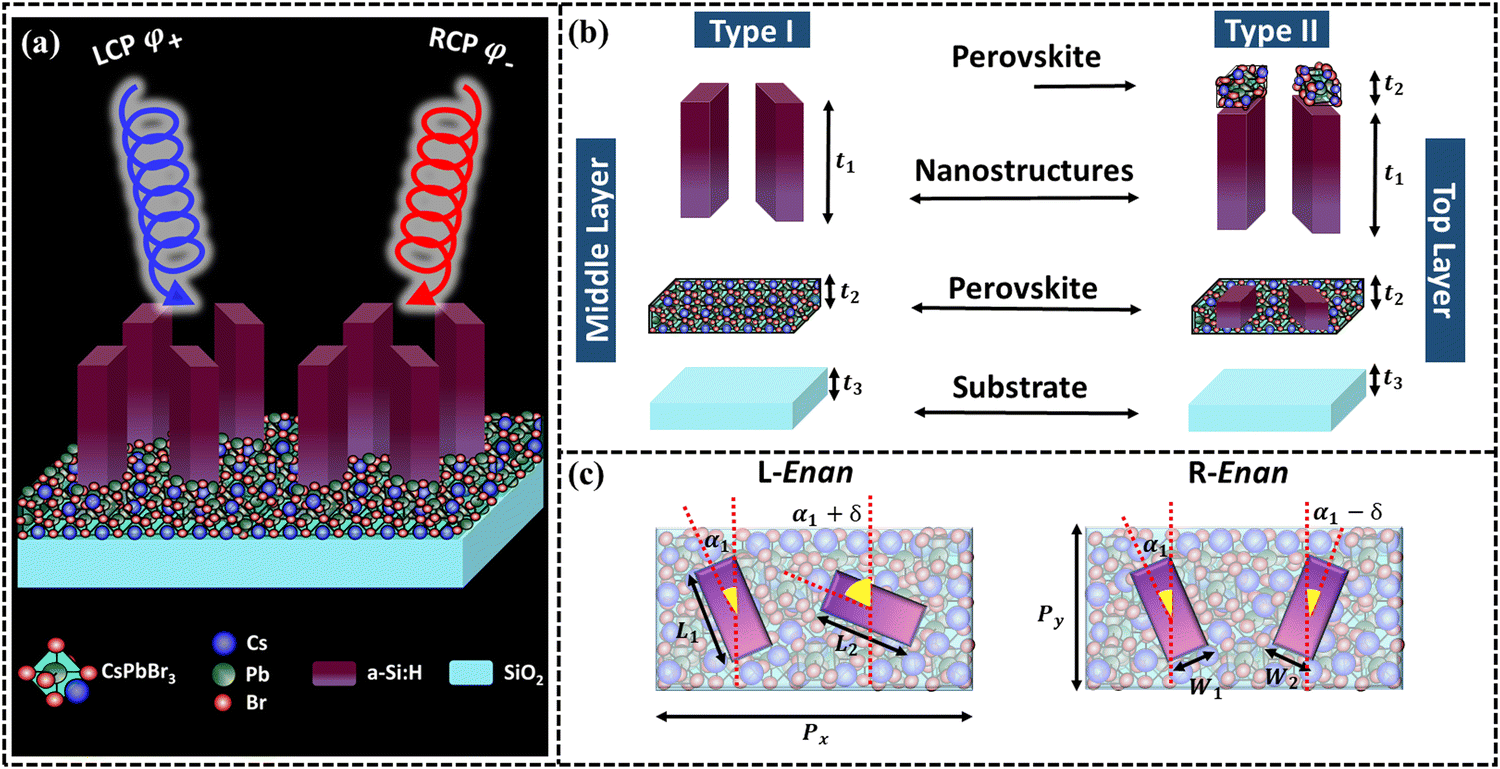 | ||
| Fig. 1 The schematic representation of the proposed perovskite chiral metasurface. (a) A pictorial description of the proposed perovskite chiral meta-nanosurface's working principle provides a spin-dependent optical response on the interaction of circularly polarized light in the broadband visible spectrum. (b) Two cases to design a superstructure integrating perovskite: (Type I) as a middle layer, placed between the substrate and chiral nanostructures, (Type II) as a top layer, placed on the top of the nanostructures. (c) The top view of the building block of the proposed perovskite chiral meta-nanosurface, along with design variables. L-Enan and R-Enan denote the left-handed and right-handed enantiomer of the perovskite chiral building block. | ||
The top view of the superstructural chiral enantiomers and design parameters are shown in Fig. 1(c). L-Enan and R-Enan denote the left-handed and right-handed enantiomer of the perovskite chiral superstructure, respectively. Both are mirror images of each other but not superimposable. For the proposed diatomic geometry, the relative rotation angle (δ) between the nano-fins defines the handedness of the enantiomer. To satisfy the chirality condition (breaking n-fold rotational symmetry and mirror symmetry), for L-Enan, the relative rotation angle δ = 45° whereas for R-Enan δ = −45°. The finite difference time domain (FDTD) method optimizes the chiral superstructure using full-wave electromagnetic simulations. The periodic boundaries are used in the x- and y-plane, whereas the perfect matched layer (PML) boundaries are in the z-plane. The parametric sweep analysis concluded the optimal design parameters for the perovskite chiral meta-nanosurface as given in Table S1 (ESI†).
3. Results and discussion
3.1. Realization of superstructural chirality
The full wave electromagnetic simulations for the L-Enan perovskite chiral superstructure demonstrate the maximum cross-polarized transmittance efficiency of 50% for LCP and negligible cross-polarization efficiency of 5% for the opposite handedness at broadband visible wavelengths, indicating giant superstructural chirality, as shown in Fig. 2(a). Due to the extra degree of freedom in the selected diatomic chiral geometry based on achiral nano-fins, it shows a broadband response at visible wavelengths. TRL and TLR show the RCP transmission for LCP illumination and LCP transmission for RCP illumination, respectively. To assess the role of the perovskite layer in influencing the giant chiro-optical responses, simulations were conducted with and without placing the perovskite layer. In Fig. 2(b), the optical responses for both scenarios are depicted: one where the perovskite layer is absent (without) and the other where the perovskite layer is incorporated (middle). The results indicate that without perovskite integration, some level of chirality is observed; however, not significantly higher, especially at the broadband wavelengths. Notably, the highest chirality is achieved within the broadband visible spectrum when the perovskite layer is strategically positioned as the middle layer in the structure. This perovskite placement plays a pivotal role in enhancing and optimizing the chiro-optical responses, particularly in the broad visible spectrum. However, it is important to note that the literature contains a variety of design strategies for creating perovskite chiral metasurfaces. As a result, for a more comprehensive understating, a further comparison is presented for both configurations discussed in Fig. 1(b). This comparison examines the performance of perovskite chiral metasurfaces with perovskite placed as the middle layer (middle) and with perovskite overcoated on the chiral nanostructure-based metasurface (top), as shown in Fig. 2(c). In comparison, it becomes evident that both scenarios demonstrate nearly similar intensity of chirality. However, a noteworthy distinction arises in the middle layer case, where more extensive and broader peaks are observed. This configuration results in a chiral response that covers a wide range of wavelengths, enhancing the performance of the metasurface for various optical applications.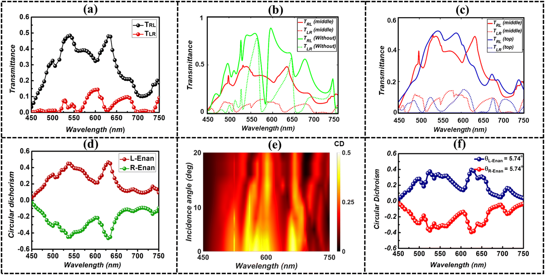 | ||
| Fig. 2 Realization of superstructural chirality. (a) The maximum transmittance for LCP incident light, whereas the minimum transmittance for RCP light introduces superstructural chirality in the broadband visible regime. TRL and TLR show the RCP transmission for LCP illumination and LCP transmission for RCP illumination, respectively. (b) The comparison of the difference in the absorption of the incident CP light for the two scenarios, i.e., without placing the perovskite layer and integrating the perovskite with the nanostructures as a middle layer. (c) The performance comparison of both strategies for achieving the maximum chirality, i.e., in the first case (Type I), sandwiching the perovskite layer in the middle of the nanostructures and the substrate, whereas in the second case (Type II), placing the perovskite layer on the top of the nanostructures. (d) The circular dichroism (CD) behavior of the perovskite chiral meta-nanosurface L-Enan and R-Enan. (e) CD demonstrated in simultaneous comparison with wavelength and the oblique incident angle of light. (f) CD analysis of both perovskite chiral enantiomers for the specific incident angle of 5.74° as a proof of concept for the experimental demonstration when the objective lens with a numerical aperture (NA) of 0.1 was used to focus the metasurface. | ||
In the accompanying analysis, the optical responses for without and with perovskite layer (positioned as the top and bottom layer) are provided in Fig. S2 (ESI†). The comparative analysis in the context of design strategies involving perovskite integration precedes the selection of the superstructure configuration in which the perovskite layer is employed as a middle layer (Type I). With the selection in consideration, it's worth noting that most of the results presented in this manuscript are elucidated with a focus on the Type I design strategy. Fig. S3 and S4 (ESI†) depict the absorption and the reflection for the L-Enan chiral superstructure, respectively. As evident from the handedness of L-Enan and obtained giant non-linear transmission, maximum absorption or reflection should be achieved for RCP illumination. For CP illumination, the spin-selective absorption is observed with maximum intensity for RCP illumination compared to LCP incident light. Similarly, some reflection was also observed for RCP illumination and almost negligible reflections for LCP incident light. Conversely, for the case of R-Enan, the situation would be opposite with maximum absorption and some reflection occurring for the LCP illumination. This distinction illustrates the spin-selective optical responses of the proposed perovskite chiral metasurface based on the incident CP light.
To check the final obtained chirality, circular dichroism (CD) for both L-Enan and R-Enan shows a wide range absorption difference for LCP and RCP illumination with a significant CD of 48% (Fig. 2(d)). CD is defined as the difference between cross-polarized transmittance for LCP and RCP illuminations. A perovskite layer with a precisely chosen thickness of 100 nm is placed in the proposed chiral perovskite metasurface. The variation in CD concerning different thicknesses of the perovskite material is illustrated in Fig. S5 (ESI†). These findings underscore that the maximum CD efficiency is attained around the perovskite thickness value of 100 nm. While there is also notable CD efficiency for the 532 nm wavelength within the thickness range of 0–10 nm, it is crucial to emphasize that the primary objective is to utilize the perovskite layer to enhance CD across the broadband spectrum, rather than focusing solely on selective wavelengths in the visible regime. This overarching goal is elucidated in Fig. 2(b), which provides a comprehensive comparison of chiral transmission with and without the perovskite layer. Moreover, CD analysis is also performed based on the incident angle of light. For chiral metasurface-based applications, oblique incidence provides a more realistic and comprehensive understanding of real-world scenarios, as the light can interact with metasurfaces from various angles except the normal incident angle. Fig. 2(e) demonstrates the CD as a function of wavelength and the incident angle up to 20°. It is noticeable that the designed perovskite chiral meta-nanosurface can generate significant CD even at an oblique incident angle. Meanwhile, for the experimental proof of concept, the CD plotted at an oblique incident angle of 5.74° had relevance to the numerical aperture (NA) of 0.1 of the objective lens when used to focus the light at the metasurface. These results show that the proposed perovskite chiral meta-nanosurface works well with significant CD efficiency at oblique incident angles due to its unique ability to manipulate the polarization of light.
3.2. Spatial distribution of strong electric and magnetic fields with giant optical chirality
The giant superstructural chirality obtained for the proposed perovskite chiral meta-nanosurface is demonstrated in terms of electric and magnetic field distributions for CP illuminations of L-Enan. Fig. 3 illustrates the electric and magnetic fields for the working wavelengths of 488 nm, 532 nm, and 633 nm. The strong constructive interference of the electric field distribution for LCP (Fig. 3(a)–(c)) and the strong destructive interference for RCP illumination (Fig. 3(d)–(f)) validate the giant superstructural chirality. Similarly, the magnetic field distribution shows the contribution towards giant superstructural chirality based on the strong coupling for LCP (Fig. 3(g)–(i)) and the weak coupling for RCP illumination (Fig. 3(j)–(l)).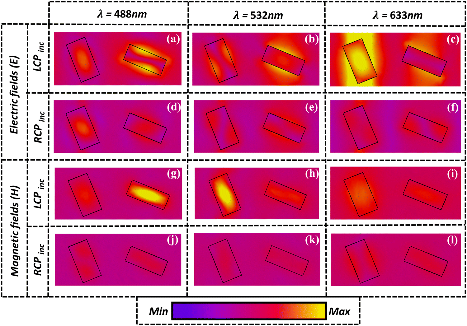 | ||
| Fig. 3 Spatial distribution of strong electric and magnetic fields with giant optical chirality. (a) Optical chirality in terms of electromagnetic field responses of the perovskite chiral meta-nanosurface (L-Enan) for the visible wavelengths. The maximum electric and magnetic fields for LCP illumination at (a) and (g) 488 nm, (b) and (h) 532 nm, and (c) and (i) 633 nm validate the realization of maximum transmission for LCP light. In contrast, the minimum electric and magnetic fields for RCP illumination at (d) and (j) 488 nm, (e) and (k) 532 nm, and (f) and (l) 633 nm validate the realization of maximum absorption for RCP light. | ||
In the meantime, considering the Type-I configuration, electric and magnetic field distributions are demonstrated in the xz-plane at the working wavelengths (Fig. S6, ESI†), showing the presence of strong coupling and higher order resonances for LCP illumination. In contrast, the coupling is notably weaker when RCP light is incident. Likewise, the electric and magnetic field distributions for the Type-II approach also demonstrate the presence of higher-order multipoles and strong coupling at the working wavelengths for LCP illumination (Fig. S7, ESI†). However, compared to the Type-I approach, weak electromagnetic field distributions and more absorption are observed for LCP at the longer wavelengths in the visible regime, which validates the chiro-optical transmission results for CP illumination. Moreover, in the red wavelength region, weak electromagnetic field distributions and more absorption for LCP are observed compared to the bottom approach.
3.3. Multipolar circular dichroism validating strong superstructural chirality
The scattering cross-section of the perovskite nano-structured meta-platform allows the multipoles to be decomposed to identify the strength and impact of the electromagnetic field and current distributions accountable for the giant superstructural chiro-optical effects (Fig. 4).60–62 The multipolar scattering demonstrated as a function of wavelength in terms of circular dichroism involves the total scattering (Fig. 4(a)), electric dipole (ED) dichroism (Fig. 4(b)), magnetic dipole (MD) dichroism (Fig. 4(c)), toroidal dipole (TD) dichroism (Fig. 4(d)), electric quadrupole (EQ) dichroism (Fig. 4(e)), and magnetic quadrupole (MQ) dichroism (Fig. 4(f)). The total scattering dichroism is defined as CDTot. Scattering = (DipoleE,M + QuadrupoleE,M + Toroidal)LCP − (Dipole(E,M) + Quadrupole(E,M) + Toroidal)RCP, the difference between individual scattering components for LCP and RCP illuminations. Notably, the ED scattering exhibits dominance at almost all visible wavelengths, with significant efficiency observed around the green wavelength region.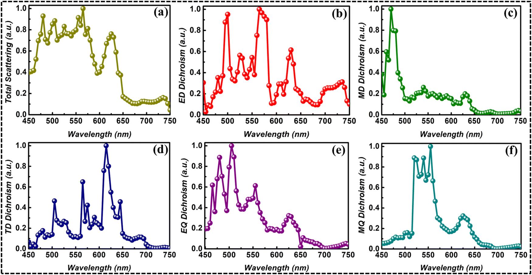 | ||
| Fig. 4 Multipolar circular dichroism validating strong superstructural chirality. (a) The total scattering in terms of CD incorporating all multipolar resonances. The contribution of individual multipole CD towards giant superstructural chirality: (b) the electric dipole (ED) as a function of wavelength; (c) the magnetic dipole (MD) as a function of wavelength; (d) the toroidal dipole (TD) as a function of wavelength; (e) the electric quadrupole (EQ) as a function of wavelength; (f) the magnetic quadrupole (MQ) as a function of wavelength showing CD dominance at different wavelengths in the visible regime. | ||
Likewise, EQ scattering (induced due to the complex interaction of electromagnetic fields and the presence of chirality-induced structures) displays notable efficiency at nearly all visible wavelengths, with a pronounced contribution in the green and blue regions. The MD and MQ scattering components dominate in the blue and green wavelength regions, respectively. In contrast, TD scattering makes a substantial contribution to the giant chiro-optical effects at the red wavelength region compared to other wavelengths in the visible regime. These multipolar scattering patterns provide valuable insights into the distribution of electric and magnetic fields in the xy- and xz-planes. Besides, the total scattering curve in Fig. 4(a) incorporates the summation of constructive and destructive interference of all multipolar components for LCP and RCP illumination, respectively. This total multipolar decomposition resembles the circular dichroism plots in Fig. 2(d) and validates the generation of giant superstructural chiro-optical effects in a perovskite dielectric chiral meta-nanosurface.
3.4. Discussion
The circular dichroism in millidegrees (mdeg) demonstrates the significant value obtained for the proposed perovskite-integrated chiral metasurface at almost all the visible wavelengths, with the maximum and the average achievable efficiency being ∼42934 and ∼27000, respectively (Fig. 5(a)). Meanwhile, the anisotropy factor (gcd) in Fig. 5(b) demonstrates the highest anisotropy factor of 1.55 compared to the reported works and the average value is ∼0.95. The anisotropy factor quantifies the degree of ellipticity of a linearly polarized light after passing through the chiral medium. The CD (mdeg) and the gcd values are obtained here using the formulation as expressed in eqn (1) and (2):57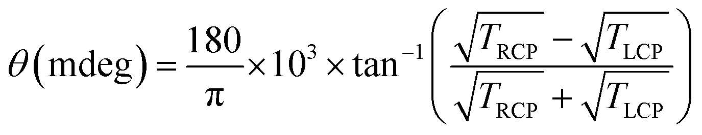 | (1) |
 | (2) |
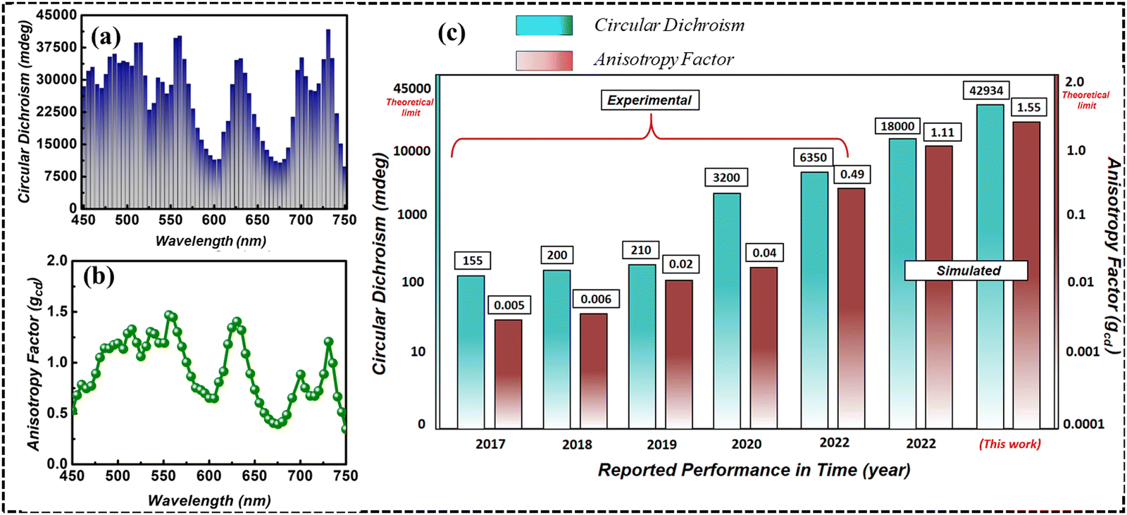 | ||
| Fig. 5 Performance comparison of the structural chirality and the anisotropy factor. (a) The circular dichroism in millidegrees upon the broadband interacting optical wavelengths. (b) The designed perovskite chiral meta-nanosurface's anisotropy factor (gcd) is depicted at the broadband visible wavelength. (c) Comparison of our work with the performance of already reported results. Ahn et al., in 2017, inquired about the chiroptical characteristics of chiral perovskites with 2D thin films, disclosing the anisotropy factor (gcd) of 0.005 and circular dichroism CD of 155 mdeg.63 In 2018, Long et al. reported reduced dimensional chiral perovskites using halide engineering, realizing gcd of 0.006 and a CD of 200 mdeg.62 Moving on, Chen et al. obtained a CD of 210 mdeg and gcd of 0.02 using a 1D perovskite film in 2019.65 In 2020, using a morphologically engineered 1D chiral perovskite a CD of 3200 mdeg and asymmetry factor gcd of 0.04 were reported.66 Recently, in 2022, Long et al. experimentally illustrated the highest superstructural chirality with remarkable CD and gcd of 6350 mdeg and 0.49, respectively.57 Meanwhile, the simulated reported CD and gcd factor values were ∼18000 and 1.11, respectively. The proposed perovskite meta-nanosurface with superstructural chirality obtained a maximum simulated CD of 42934 and gcd of 1.55, almost reaching the theoretical limit of CD and the anisotropy factor, which is 45000 mdeg and 2.0, respectively. | ||
The comparison includes the selectively reported performances in the literature for the hybrid perovskites based on structural and superstructural design strategies for numerous applications. Starting from 2017, Ahn et al. demonstrated the 2D thin film of the hybrid perovskite incorporating the chiral organic molecules, disclosing the gcd of 0.005 and CD of 155 mdeg for potential applications in advanced optics and spintronics.63 The crystalline orientation and the thickness of the perovskite film change the intensity of the CD signal. In 2018, a halide-engineered reduced dimensional chiral perovskite demonstrated for spin-polarized photon absorption and spin-polarized photoluminescence through combined strategies of chirality transfer and energy funneling, realizing gcd of 0.006 and a CD of 200 mdeg.64 Another work reported in 2019 was based on a 1D flexible chiral hybrid perovskite film incorporating chiral organic for circularly polarized light detection to obtain a CD of 210 mdeg and gcd of 0.02.65 Furthermore, in 2020, a morphologically engineered 1D lead halide perovskite composed of naphthylethylamine based chiral organic cations was reported to achieve CD of 3200 mdeg and gcd of 0.04.66
More recently, in 2022, using perovskite superstructural chirality reported the highest CD and gcd of 6350 mdeg and 0.49, respectively.57 A gammadion geometry was adopted to get the proposed chiro-optical results. Moreover, the reported CD and gcd factor value with theoretical simulation was ∼18000 and 1.11, respectively. However, compared to the above-reported works, our approach employs a diatomic chiral geometry built upon achiral nano-fins, introducing additional degrees of freedom. This strategic design choice leads to the attainment of the highest simulated values of circular dichroism (CD) and anisotropy factor (gcd) across a broad range of optical wavelengths within the visible spectrum. Notably, our diatomic chiral metasurface, featuring nano-fins, outperforms comparable metasurfaces reported in the literature that share the same design geometry but lack the integration of the perovskite.3,7 Based on the proposed perovskite chiral meta-nanosurface, these reported values are significantly higher and almost reach the theoretical limit that can be evaluated using eqn (1) and (2).57 To experimentally validate the proposed perovskite-integrated chiral metasurfaces, we have included the perspective fabrication procedure based on the reported literature (ESI†).11 Hence, instead of a chemical approach, the carefully engineered chiral nanostructures with perovskites can enhance broadband spin-dependent absorption, lead to giant superstructural chirality, and paving the way for potential applications in chiral photonics.
4. Conclusion
This work demonstrated a planar all-dielectric nanostructure-based metasurface integrated with perovskite to realize exceptional superstructural chirality at the broadband visible regime. Considering the previously discussed design strategies, we designed diatomic chiral nanostructures accumulating the properties of perovskites using two structural configurations (Type I and Type II). However, the Type I configuration stands out for its ability to deliver chiro-optical responses across a broad spectrum of visible wavelengths, ultimately enhancing the metasurface performance. Hence, it has achieved remarkable chirality with a maximum anisotropy factor value of ∼1.55 and a circular dichroism value of ∼42934 mdeg. Meanwhile, the average values at the broad visible wavelengths for the anisotropy factor and circular dichroism are ∼0.95 and ∼27000 mdeg. The electric and magnetic field distributions validate the giant superstructural chirality and show extraordinary improvement in chiro-optical effects by nanostructural engineering. Moreover, the generation of giant chiro-optical effects is validated by the individual contribution of the multipolar resonance dichroism. Based on the design methodology and the results, this work shows potential applications in perovskite chiral photonics,67 tunable meta-devices,68–70 spintronic devices,71,72 and optoelectronics.68,70,72 Furthermore, this concept based on integrating chiral nanostructural engineering with perovskites can be used to design chiral metasurfaces with giant chirality in ultraviolet and infrared regimes, incorporating tunable properties.73–76
Conflicts of interest
The authors declare no conflict of interest.Acknowledgements
This research was supported by Kyungpook National University Research Fund, 2022.References
- X. Ma, M. Pu, X. Li, Y. Guo, P. Gao and X. Luo, Nanomaterials, 2017, 7 Search PubMed.
- H. S. Khaliq, A. Nauman, J. W. Lee and H. R. Kim, Adv. Opt. Mater., 2023, 2300644 CrossRef CAS.
- H. S. Khaliq, I. Kim, J. Kim, D. K. Oh, M. Zubair, K. Riaz, M. Q. Mehmood and J. Rho, Adv. Opt. Mater., 2021, 9, 2002002 CrossRef CAS.
- T. Naeem, J. Kim, H. S. Khaliq, J. Seong, M. T. S. Chani, T. Tauqeer, M. Q. Mehmood, Y. Massoud and J. Rho, Adv. Opt. Mater., 2023, 11, 2202278 CrossRef CAS.
- H. Saad Khaliq, J. Kim, T. Naeem, K. Riaz, T. Badloe, J. Seong, J. Akbar, M. Zubair, M. Q. Mehmood, Y. Massoud, J. Rho, H. S. Khaliq, Y. Massoud, J. Kim, T. Badloe, J. Seong, J. Rho, T. Naeem, K. Riaz, M. Zubair, M. Q. Mehmood and J. Akbar, Adv. Opt. Mater., 2022, 10, 2201175 CrossRef.
- A. Asad, J. Kim, H. S. Khaliq, N. Mahmood, J. Akbar, M. T. S. Chani, Y. Kim, D. Jeon, M. Zubair, M. Q. Mehmood, Y. Massoud and J. Rho, Nanoscale Horiz., 2023, 8, 759–766 RSC.
- H. S. Khaliq, I. Kim, A. Zahid, J. Kim, T. Lee, T. Badloe, Y. Kim, M. Zubair, M. Zubair, K. Riaz, K. Riaz, M. Q. Mehmood, M. Q. Mehmood, J. Rho, J. Rho, J. Rho and J. Rho, Photonics Res., 2021, 9, 1667–1674 CrossRef.
- H. S. Khaliq, M. R. Akram, K. Riaz, K. Riaz, M. A. Ansari, J. Akbar, J. Zhang, W. Zhu, D. Zhang, X. Wang, M. Zubair, M. Q. Mehmood and M. Q. Mehmood, Opt. Express, 2021, 29, 3230–3242 CrossRef CAS PubMed.
- G. Long, R. Sabatini, M. I. Saidaminov, G. Lakhwani, A. Rasmita, X. Liu, E. H. Sargent and W. Gao, Nat. Rev. Mater., 2020, 5, 423–439 CrossRef.
- J. Tian, G. Adamo, H. Liu, M. Klein, S. Han, H. Liu and C. Soci, Adv. Mater., 2022, 34, 2109157 CrossRef CAS PubMed.
- I. Vinçon, F. J. Wendisch, D. De Gregorio, S. D. Pritzl, Q. A. Akkerman, H. Ren, L. De, S. Menezes, S. A. Maier and J. Feldmann, ACS Photonics, 2022, 9, 3506–3514 CrossRef.
- W. Qin, H. Xu and B. Hu, ACS Photonics, 2017, 4, 2821–2827 CrossRef CAS.
- J. Wang, C. Zhang, H. Liu, R. McLaughlin, Y. Zhai, S. R. Vardeny, X. Liu, S. McGill, D. Semenov, H. Guo, R. Tsuchikawa, V. V. Deshpande, D. Sun and Z. V. Vardeny, Nat. Commun., 2019, 10, 1–6 CrossRef PubMed.
- Y. Liu, L. Collins, R. Proksch, S. Kim, B. R. Watson, B. Doughty, T. R. Calhoun, M. Ahmadi, A. V. Ievlev, S. Jesse, S. T. Retterer, A. Belianinov, K. Xiao, J. Huang, B. G. Sumpter, S. V. Kalinin, B. Hu and O. S. Ovchinnikova, Nat. Mater., 2018, 17, 1013–1019 CrossRef CAS PubMed.
- C. Zhang, D. Sun, C. X. Sheng, Y. X. Zhai, K. Mielczarek, A. Zakhidov and Z. V. Vardeny, Nat. Phys., 2015, 11, 427–434 Search PubMed.
- D. Di Nuzzo, L. Cui, J. L. Greenfield, B. Zhao, R. H. Friend and S. C. J. Meskers, ACS Nano, 2020, 14, 7610–7616 CrossRef CAS PubMed.
- D. Ayuso, O. Neufeld, A. F. Ordonez, P. Decleva, G. Lerner, O. Cohen, M. Ivanov and O. Smirnova, Nat. Photonics, 2019, 13, 866–871 CrossRef CAS.
- G. Long, G. Adamo, J. Tian, M. Klein, H. N. S. Krishnamoorthy, E. Feltri, H. Wang and C. Soci, Nat. Commun., 2022, 13, 1551 CrossRef CAS PubMed.
- H. S. Khaliq, I. Kim, K. Riaz, T. Naeem, M. Zubair, J. Rho and M. Q. Mehmood, J. Phys. Conf. Ser., 2021, 2015, 012060 CrossRef CAS.
- H. S. Khaliq, M. R. Akram, K. Riaz, M. A. Ansari, J. Akbar, J. Zhang, W. Zhu, D. Zhang, X. Wang, M. Zubair and M. Q. Mehmood, Opt. Express, 2021, 29, 3230 CrossRef CAS PubMed.
- Z. L. Deng, J. Deng, X. Zhuang, S. Wang, K. Li, Y. Wang, Y. Chi, X. Ye, J. Xu, G. P. Wang, R. Zhao, X. Wang, Y. Cao, X. Cheng, G. Li and X. Li, Nano Lett., 2018, 18, 2885–2892 CrossRef CAS PubMed.
- Q. Wang, E. Plum, Q. Yang, X. Zhang, Q. Xu, Y. Xu, J. Han and W. Zhang, Light Sci. Appl., 2018, 7, 25 CrossRef PubMed.
- W. Ye, F. Zeuner, X. Li, B. Reineke, S. He, C. W. Qiu, J. Liu, Y. Wang, S. Zhang and T. Zentgraf, Nat. Commun., 2016, 7, 11930 CrossRef CAS PubMed.
- S. Jahani and Z. Jacob, Nat. Nanotechnol., 2016, 11, 23–36 CrossRef CAS PubMed.
- S. Zanotto, A. Tredicucci, D. Navarro-Urrios, M. Cecchini, G. Biasiol, D. Mencarelli, L. Pierantoni and A. Pitanti, Adv. Opt. Mater., 2020, 8, 1901507 CrossRef CAS.
- K. Tanaka, D. Arslan, S. Fasold, M. Steinert, Jurgen Sautter, M. Falkner, T. Pertsch, M. Decker and I. Staude, ACS Nano, 2020, 14, 15926–15935 CrossRef CAS PubMed.
- J. García-Guirado, M. Svedendahl, J. Puigdollers and R. Quidant, Nano Lett., 2020, 20, 585–591 CrossRef PubMed.
- A. Y. Zhu, W. T. Chen, A. Zaidi, Y. W. Huang, M. Khorasaninejad, V. Sanjeev, C. W. Qiu and F. Capasso, Light: Sci. Appl., 2018, 7, 17158 CrossRef CAS PubMed.
- Y. Chen, J. Gao and X. Yang, Nano Lett., 2018, 18, 520–527 CrossRef CAS PubMed.
- Y. Zhao, A. N. Askarpour, L. Sun, J. Shi, X. Li and A. Alù, Nat. Commun., 2017, 8, 1–8 CrossRef CAS PubMed.
- J. K. Gansel, M. Thiel, M. S. Rill, M. Decker, K. Bade, V. Saile, G. Von Freymann, S. Linden and M. Wegener, Science, 2009, 325, 1513–1515 CrossRef CAS PubMed.
- M. Hentschel, M. Schäferling, T. Weiss, N. Liu and H. Giessen, Nano Lett., 2012, 12, 2542–2547 CrossRef CAS PubMed.
- B. Gholipour, G. Adamo, D. Cortecchia, H. N. S. Krishnamoorthy, M. D. Birowosuto, N. I. Zheludev, C. Soci, B. Gholipour, G. Adamo, H. N. S. Krishnamoorthy, N. I. Zheludev, C. Soci, D. Cortecchia and M. D. Birowosuto, Adv. Mater., 2017, 29, 1604268 CrossRef PubMed.
- Y. Gao, C. Huang, C. Hao, S. Sun, L. Zhang, C. Zhang, Z. Duan, K. Wang, Z. Jin, N. Zhang, A. V. Kildishev, C. W. Qiu, Q. Song and S. Xiao, ACS Nano, 2018, 12, 8847–8854 CrossRef CAS PubMed.
- Y. Fan, Y. Wang, N. Zhang, W. Sun, Y. Gao, C. W. Qiu, Q. Song and S. Xiao, Nat. Commun., 2019, 10, 1–8 CrossRef PubMed.
- Y. Chen, J. Gao and X. Yang, Nano Lett., 2018, 18, 520–527 CrossRef CAS PubMed.
- C. Zhang, S. Xiao, Y. Wang, Y. Gao, Y. Fan, C. Huang, N. Zhang, W. Yang and Q. Song, Laser Photon. Rev., 2019, 13, 1900079 CrossRef.
- G. Adamo, H. N. Swaha Krishnamoorthy, D. Cortecchia, B. Chaudhary, V. Nalla, N. I. Zheludev and C. Soci, Nano Lett., 2020, 20, 7906–7911 CrossRef CAS PubMed.
- Z. Li, J. S. T. Smalley, R. Haroldson, D. Lin, R. Hawkins, A. Gharajeh, J. Moon, J. Hou, C. Zhang, W. Hu, A. Zakhidov and Q. Gu, ACS Photonics, 2020, 7, 1754–1761 CrossRef CAS.
- E. Tiguntseva, A. Chebykin, A. Ishteev, R. Haroldson, B. Balachandran, E. Ushakova, F. Komissarenko, H. Wang, V. Milichko, A. Tsypkin, D. Zuev, W. Hu, S. Makarov and A. Zakhidov, Nanoscale, 2017, 9, 12486–12493 RSC.
- N. Pourdavoud, S. Wang, A. Mayer, T. Hu, Y. Chen, A. Marianovich, W. Kowalsky, R. Heiderhoff, H.-C. Scheer, T. Riedl, N. Pourdavoud, T. Hu, R. Heiderhoff, T. Riedl, S. Wang, A. Mayer, H. Scheer, Y. Chen, A. Marianovich and W. Kowalsky, Adv. Mater., 2017, 29, 1605003 CrossRef PubMed.
- S. V. Makarov, V. Milichko, E. V. Ushakova, M. Omelyanovich, A. Cerdan Pasaran, R. Haroldson, B. Balachandran, H. Wang, W. Hu, Y. S. Kivshar and A. A. Zakhidov, ACS Photonics, 2017, 4, 728–735 CrossRef CAS.
- A. Y. Zhizhchenko, P. Tonkaev, D. Gets, A. Larin, D. Zuev, S. Starikov, E. V. Pustovalov, A. M. Zakharenko, S. A. Kulinich, S. Juodkazis, A. A. Kuchmizhak, S. V. Makarov, A. Y. Zhizhchenko, A. A. Kuchmizhak, P. Tonkaev, D. Gets, A. Larin, D. Zuev, S. V. Makarov, S. Starikov, E. V. Pustovalov, A. M. Zakharenko, S. A. Kulinich and S. Juodkazis, Small, 2020, 16, 2000410 CrossRef CAS PubMed.
- C. Huang, C. Zhang, S. Xiao, Y. Wang, Y. Fan, Y. Liu, N. Zhang, G. Qu, H. Ji, J. Han, L. Ge, Y. Kivshar and Q. Song, Science, 2020, 367, 1018–1021 CrossRef CAS PubMed.
- S. Brittman, S. Z. Oener, K. Guo, H. Aboliņš, A. F. Koenderink and E. C. Garnett, J. Mater. Chem. C, 2017, 5, 8301–8307 RSC.
- O. Bar-On, P. Brenner, U. Lemmer, J. Scheuer, O. Bar-On, J. Scheuer, P. Brenner and U. Lemmer, Adv. Mater. Technol., 2018, 3, 1800212 CrossRef.
- Z. Li, J. Moon, A. Gharajeh, R. Haroldson, R. Hawkins, W. Hu, A. Zakhidov and Q. Gu, ACS Nano, 2018, 12, 10968–10976 CrossRef CAS PubMed.
- H. Park, C. Ha and J. H. Lee, J. Mater. Chem. A, 2020, 8, 24353–24367 RSC.
- Y. Qin, F. F. Gao, S. Qian, T. M. Guo, Y. J. Gong, Z. G. Li, G. D. Su, Y. Gao, W. Li, C. Jiang, P. Lu and X. H. Bu, ACS Nano, 2022, 16, 3221–3230 CrossRef CAS PubMed.
- P. V. Shinde, A. Patra and C. S. Rout, J. Mater. Chem. C, 2022, 10, 10196–10223 RSC.
- B. Ai, Z. Fan and Z. J. Wong, Microsyst. Nanoeng., 2022, 8, 1–28 CrossRef PubMed.
- Y. Dong, Y. Zhang, X. Li, Y. Feng, H. Zhang, J. Xu, Y. Dong, X. Li, Y. Feng, J. Xu, Y. Zhang and H. Zhang, Small, 2019, 15, 1902237 CrossRef PubMed.
- S. Ma, Y. K. Jung, J. Ahn, J. Kyhm, J. Tan, H. Lee, G. Jang, C. U. Lee, A. Walsh and J. Moon, Nat. Commun., 2022, 13, 1–10 Search PubMed.
- J. Ma, C. Fang, C. Chen, L. Jin, J. Wang, S. Wang, J. Tang and D. Li, ACS Nano, 2019, 13, 3659–3665 CrossRef CAS PubMed.
- Y. Yang, G. Yoon, S. Park, S. D. Namgung, T. Badloe, K. T. Nam and J. Rho, Adv. Mater., 2021, 33, 2005893 CrossRef CAS PubMed.
- G. Ermolaev, A. P. Pushkarev, A. Zhizhchenko, A. A. Kuchmizhak, I. Iorsh, I. Kruglov, A. Mazitov, A. Ishteev, K. Konstantinova, D. Saranin, A. Slavich, D. Stosic, E. S. Zhukova, G. Tselikov, A. Di Carlo, A. Arsenin, K. S. Novoselov, S. V. Makarov and V. S. Volkov, Nano Lett., 2023, 23, 2570–2577 CrossRef CAS PubMed.
- G. Long, K. Adamo, J. Tian, M. Klein, H. N. S. Krishnamoorthy, E. Feltri, H. Wang and C. Soci, Nat. Commun., 2022, 13, 1–8 Search PubMed.
- R. Tao, K. Peng, L. Haeberlé, Q. Li, D. Jin, G. R. Fleming, S. K. Cohen, X. Zhang and W. Bao, Nat. Mater., 2022, 21, 761–766 CrossRef CAS PubMed.
- X. Chen, W.-G. Lu, J. Tang, Y. Zhang, Y. Wang, G. D. Scholes and H. Zhong, Nat. Photonics, 2021, 15, 813–816 CrossRef.
- Y. S. Kivshar and D. Smirnova, Optica, 2016, 3, 1241–1255 CrossRef.
- O. Wolf, S. Campione, Y. Yang and I. Brener, Sci. Rep., 2017, 7, 1–7 CrossRef CAS PubMed.
- T. Liu, R. Xu, P. Yu, Z. Wang and J. Takahara, Nanophotonics, 2020, 9, 1115–1137 CrossRef.
- J. Ahn, E. Lee, J. Tan, W. Yang, B. Kim and J. Moon, Mater. Horiz., 2017, 4, 851–856 RSC.
- G. Long, C. Jiang, R. Sabatini, Z. Yang, M. Wei, L. N. Quan, Q. Liang, A. Rasmita, M. Askerka, G. Walters, X. Gong, J. Xing, X. Wen, R. Quintero-Bermudez, H. Yuan, G. Xing, X. R. Wang, D. Song, O. Voznyy, M. Zhang, S. Hoogland, W. Gao, Q. Xiong and E. H. Sargent, Nat. Photonics, 2018, 12, 528–533 CrossRef CAS.
- C. Chen, L. Gao, W. Gao, C. Ge, X. Du, Z. Li, Y. Yang, G. Niu and J. Tang, Nat. Commun., 2019, 10, 1–7 CrossRef PubMed.
- S. Ma, J. Ahn, J. Moon, S. Ma, J. Ahn and J. Moon, Adv. Mater., 2021, 33, 2005760 CrossRef CAS PubMed.
- O. D. I. Moseley, B. Roose, S. J. Zelewski, S. Kahmann, K. Dey and S. D. Stranks, ACS Photonics, 2022, 9, 3958–3966 CrossRef CAS PubMed.
- H. Tan, L. N. Quan and M. Saliba, Nanophotonics, 2021, 10, 1941–1942 CrossRef.
- A. Karabchevsky, Light Sci. Appl., 2023, 12, 1–2 CrossRef PubMed.
- Y. Liu, F. Li and W. Huang, Matter, 2023, 6, 3165–3219 CrossRef CAS.
- A. Privitera, M. Righetto, F. Cacialli, M. K. Riede, A. Privitera, M. K. Riede, M. Righetto and F. Cacialli, Adv. Opt. Mater., 2021, 9, 2100215 CrossRef CAS.
- Q. Wei and Z. Ning, ACS Mater. Lett., 2021, 3, 1266–1275 CrossRef CAS.
- L. Zhang, C. Sun, T. He, Y. Jiang, J. Wei, Y. Huang and M. Yuan, Light Sci. Appl., 2021, 10, 1–26 CrossRef PubMed.
- W. Hu, H. Cong, W. Huang, Y. Huang, L. Chen, A. Pan and C. Xue, Light Sci. Appl., 2019, 8, 1–10 CrossRef CAS PubMed.
- M.-W. Kim, Y. Yuan, S. Jeong, J. Chong, H. Mølnås, A. Alaei, I. J. Cleveland, N. Liu, Y. Ma, S. Strauf, E. S. Aydil, A. Sahu, D. M. Kalyon, S. S. Lee, M.-W. Kim, S. Jeong, J. Chong, A. Alaei, S. S. Lee, Y. Yuan, D. M. Kalyon, H. Mølnås, I. J. Cleveland, E. S. Aydil, A. Sahu, N. Liu, Y. Ma and S. Strauf, Adv. Funct. Mater., 2022, 32, 2207326 CrossRef CAS.
- A. Valluvar Oli, Z. Li, Y. Chen and A. Ivaturi, ACS Appl. Energy Mater., 2022, 5, 14669–14679 CrossRef CAS PubMed.
Footnotes |
| † Electronic supplementary information (ESI) available. See DOI: https://doi.org/10.1039/d3ma00953j |
| ‡ These authors have contributed equally to this work. |
| This journal is © The Royal Society of Chemistry 2024 |