
 Open Access Article
 This Open Access Article is licensed under a Creative Commons Attribution-Non Commercial 3.0 Unported Licence
First principles study of WSe2 and the effect of V doping on the optical and electronic properties†
Eleonora
Pavoni
 a,
Elaheh
Mohebbi
a,
Gian Marco
Zampa
b,
Pierluigi
Stipa
a,
Luca
Pierantoni
b,
Emiliano
Laudadio
*a and
Davide
Mencarelli
b
a,
Elaheh
Mohebbi
a,
Gian Marco
Zampa
b,
Pierluigi
Stipa
a,
Luca
Pierantoni
b,
Emiliano
Laudadio
*a and
Davide
Mencarelli
b
aDepartment of Matter, Environmental Sciences, and Urban Planning, Marche Polytechnic University, 60131 Ancona, Italy. E-mail: e.laudadio@staff.univpm.it
bInformation Engineering Department, Marche Polytechnic University, 60131 Ancona, Italy
First published on 19th December 2023
Abstract
Tungsten diselenide WSe2 is a material with an intriguing character that has captivated the attention of researchers; in this study, an ab initio analysis is presented that focuses on the optical and electronic properties of WSe2. The study made use of density functional theory (DFT) by employing the Perdew–Burke–Ernzerhof (PBE) generalized gradient approximation (GGA) density functional and PseudoDojo pseudopotential. The study looked at the properties of both bulk and monolayer WSe2 to determine how the number of layers affects the properties of the material. To further investigate the properties of WSe2, four different systems based on vanadium doped-WSe2 were analyzed from the optical and electronic points of view. The systems contained different percentages of V: (i) WSe2:V 1.4%, (ii) WSe2:V 2.8%, (iii) WSe2:V 5.6%, and (iv) WSe2:V 11.2%. The introduction of vanadium brought about a reduction of the bandgap and a global shift of the projected density of states. The valence band maximum (VBM) also crossed the Fermi level, which is consistent with the p-type nature of vanadium doping. Furthermore, the absorption spectra changed in terms of the position and the intensity of the optical transition as a result of vanadium introduction.
Introduction
Terahertz (THz) technology has gained significant interest in recent years due to its unique ability to bridge the gap between electronics and optics.1 In this context, tungsten diselenide (WSe2) has emerged as a promising material and a good candidate for the next generation of devices.2,3Tungsten diselenide is a two-dimensional (2D) transition metal dichalcogenide (TMD) that has attracted significant attention from the scientific community due to its unique structural, optical, and electronic properties.4–6 As a member of the TMD group of compounds, WSe2 exhibits intriguing characteristics, making it a promising material for a wide range of applications, including optoelectronics, energy storage,5,7 and THz communications.8 Tungsten diselenide possesses a hexagonal crystal structure, belongs to P63/mmc space group, and is isotypic with hexagonal MoS2.9,10 However, compared to Mo, W is more abundant as an element in the Earth's crust and thus cheaper, and less toxic.8 The significantly larger size of W atoms can substantially tune the TMD properties. The WSe2 structure consists of a sandwich-like arrangement 2H-WSe2 (where two sheets per unit cell characterize the 2H phase) of tungsten atoms between two layers of selenium atoms; in particular, each layer of WSe2 is composed of a hexagonal lattice of atoms, in which each tungsten atom is coordinated with six selenium atoms and each selenium is bonded to three tungsten units. The strong covalent bonding within the layers gives rise to the robust nature of WSe2 and the van der Waals interactions keep together the different layers.8,11 In addition to the typical semiconducting hexagonal structure, another polymorph of WSe2 is known (1T-WSe2), which is based on a tetragonal symmetry with one WSe2 layer per unit cell, which results in a less stable configuration compared to 2H-WSe2.12
The 2D nature of WSe2 results in its unique mechanical properties.13 It exhibits excellent flexibility and can be easily exfoliated into single or few-layer sheets. The monolayer WSe2 has a direct bandgap of 1.7 eV, highly suitable for optoelectronic applications.6,14 WSe2 exhibits peculiar optical properties deriving from its quantum confinement effects in the 2D regime. The bandgap of WSe2 can be tuned by changing the number of layers, ranging from the visible to the near-infrared spectrum; moreover, the direct bandgap nature of monolayer WSe2 allows for efficient light emission and absorption.14,15 Excitonic effects dominate the optical response of WSe2.6 Excitons, bound electron–hole pairs, are strongly confined in the 2D layer, leading to enhanced light–matter interactions: the large exciton binding energy in WSe2 results in robust exciton formation at room temperature, making it ideal for applications in photonics and solar cells. Moreover, the strong light–matter interaction and the ability to engineer the bandgap via strain or doping provide opportunities for tunable optical properties in devices based on WSe2.15,16
Together with the optical properties, even the electronic properties of WSe2 are significantly influenced by its 2D structure and quantum confinement effects. WSe2 exhibits a direct bandgap in the monolayer form, enabling efficient charge carrier generation and transport; additionally, the presence of a bandgap makes it an attractive material for field-effect transistors and other electronic devices.2,8,17 WSe2 possesses several characteristics that make it an excellent candidate for THz applications. Firstly, WSe2 exhibits strong light–matter interactions, allowing for efficient absorption and emission of THz radiation. Its unique band structure, consisting of a direct bandgap, enables efficient carrier generation and manipulation in the THz regime. Moreover, WSe2 possesses good carrier mobility and low effective mass, contributing to its capability to support high-frequency electronic and optoelectronic devices.2,3 WSe2 can be utilized for both THz generation and detection. In terms of THz generation, the optical pump-THz probe technique can be employed using WSe2 as a photoconductive material. By illuminating WSe2 with a short-pulsed laser, ultrafast carrier dynamics are induced, resulting in the emission of THz radiation.18 The properties of WSe2 and WS2 have been evaluated by other authors in the context of heterostructures, for hydrogen production from water splitting in the Z-scheme module as well as for photonics and electronic applications.19–22 Moreover, the properties of WSe2 can be tuned by the presence of a doping agent; in particular, the attention of recent research has been focused on vanadium doping. This is due to the capability of vanadium to replace tungsten units which results in p-type doping. The incorporation of V atoms into the crystal structure of WSe2 and the p-type nature of the V in WSe2 is already discussed in the literature.16,23 In particular, Mallet et al. identified isolated V atoms substituted on the W sites by using scanning probe microscopy techniques, and in agreement with other previous papers.23,24 Furthermore, the V atoms are electron-poor if compared to the tungsten, and the p-type doping effect is verified by Kozhakhmetov et al. who used the V:WSe2 to build a field effect transistor where the hole conduction is dominant as the amount of V is increased.16 However, a clear understanding of the optical and electronic properties of WSe2 that has undergone V doping has not already been reported. Other authors investigated the presence of vacancy defects as well as the effect of different doping agents on tungsten telluride regarding the properties of the material.25 For this purpose, here we report a study of the optical and electronic properties of WSe2 as 1 monolayer (ML) and as a bulk material. The same analysis has been considered also for WSe2 doped with different percentages of V. In particular, four different systems based on a ML of WSe2 in which V is replacing 1.4%, 2.8%, 5.8%, and 11.6% of the W, are considered. A schematic representation of the molecular structures of WSe2 and V:WSe2 is reported in Fig. 1. The systems have been first geometrically optimized and then the optical and the electronic properties have been calculated by using density functional theory (DFT). A Quantum Atomistic ToolKit (ATK) atomic-scale modeling platform has been used to model all the WSe2 structures and to perform all calculations.26–28 Our work aims to understand how the properties of such an innovative material can be modified by the presence of a doping agent such as V, already discussed in the literature and previously tested experimentally. We aim to understand how different percentages of V can help to alter the geometric structure of the material and therefore influence its optical and electronic properties in order to improve its applicability in the new generation of devices and for applications in the field of THz telecommunications.
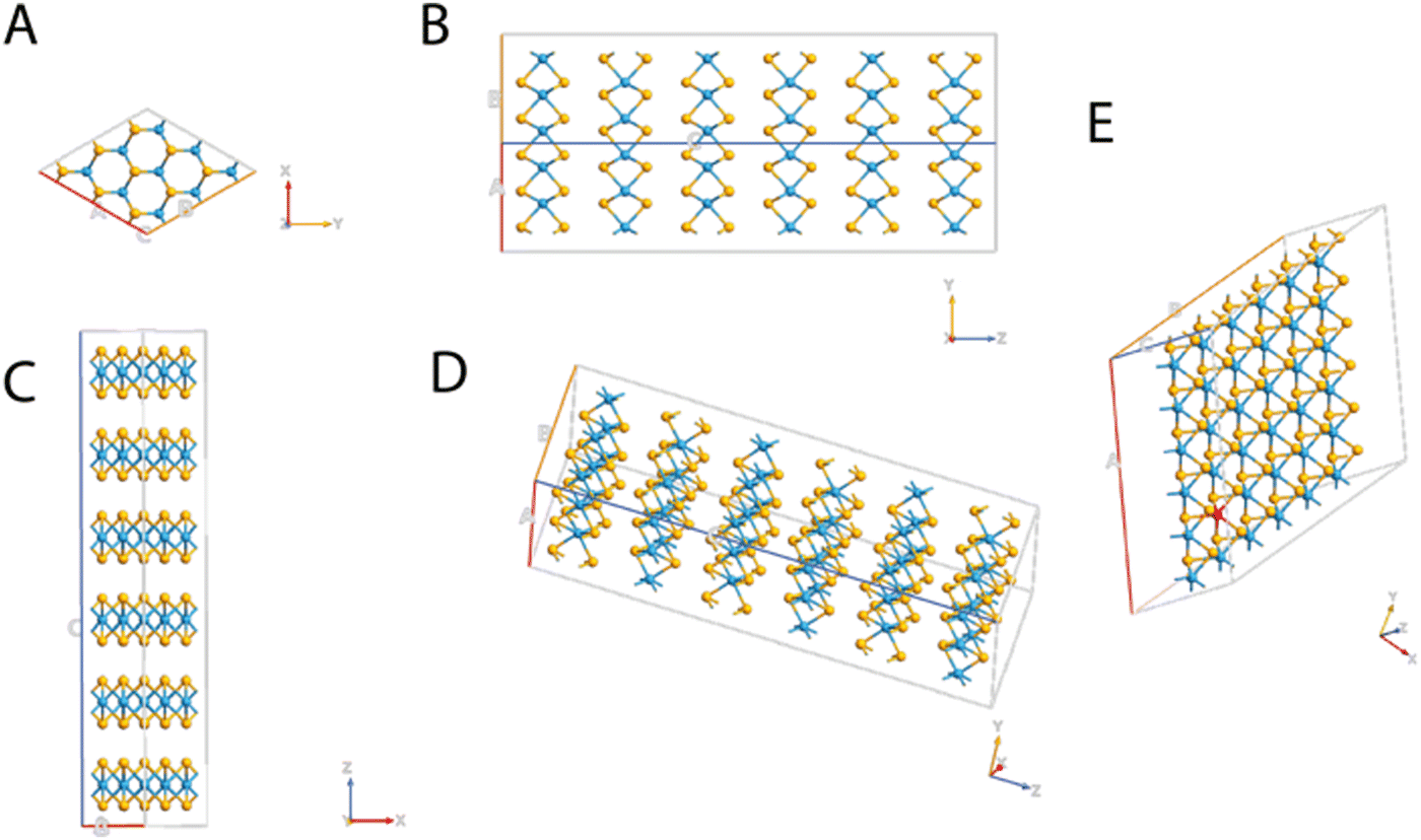 | ||
| Fig. 1 Schematic representation of the molecular structures of WSe2 from different perspectives: (A) xy plane, (B) yz plane, (C) xz plane, and (D) 3D view, and WSe2 doped with V (E). Tungsten, selenium, and vanadium are depicted in blue, yellow, and red, respectively. | ||
Results and discussion
Tungsten diselenide has a hexagonal crystal structure and is part of the P63/mmc space group.9 Furthermore, the WSe2 structure comprises a sandwich-like disposition with two sheets inside each unit cell (2H-WSe2) of tungsten atoms between two layers of selenium atoms; thus, every layer of WSe2 is composed of a hexagonal lattice of atoms, with tungsten that coordinates six selenium atoms and each selenium bonded to three tungsten units. Inside the crystal structure of WSe2 there are strong covalent bonds that hold together the W and Se atoms in each layer, conferring a robust in-plane structure, and van der Waals interactions, which keep together the different layers, presenting a graphene-like property to be easily exfoliated.8,11 In fact, the electronic configuration of the Se atoms is [Ar]3d104s24p4 and that of W atoms is [Xe]4f145d46s2; therefore, there is a fairly strong p–d orbital interaction between the W and the Se positioned in the same layer, while the interaction between neighboring sandwich layers is only weak and of van der Waals type.29 The geometrical lattice parameters, obtained after the geometry optimization, resulted in a = b = 3.528 Å and c = 12.96 Å, in line with the data already reported in the literature and with the experimental findings.14,30 The integration of V atoms into the crystal structure of WSe2 brings a p-type doping effect and it is due to the substitution of the W atoms by the V ones, as reported by other authors16,23,24,31 The effect of vanadium incorporation, even at very small doping percentages, affects the optical and electronic properties peculiarly. Fig. 2 reports the bond lengths and bond angles of the undoped and the V-doped WSe2. Both of these parameters undergo only moderate changes when V replaces W atoms. Inside the unit cell, the bond between W and Se is 2.54 Å and 2.55 Å in the undoped and V-doped samples, respectively; while the new V–Se bond is 2.49 Å, only slightly shorter. Similarly, the angle Se–W–Se moves from 80.64° to 80.16° in the undoped and V-doped samples, respectively, while the Se–V–Se bond is 80.34°.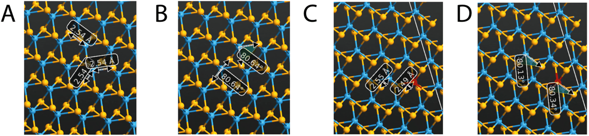 | ||
| Fig. 2 Bond lengths (A) and bond angles (B) of undoped WSe2; bond lengths (C) and bond angles (D) of V-doped WSe2. Tungsten, selenium, and vanadium are depicted in blue, yellow, and red, respectively. | ||
Band structure, bandgap, and density of the electronic states
The electronic properties of WSe2 depend on the number of layers that compose the material as demonstrated by the band structures reported in Fig. 3; as a matter of fact, the band structures of WSe2 undergo an indirect-to-direct gap when weakened to a single monolayer. The ML of WSe2 is characterized by both the valence band maximum (VBM) and conduction band minimum (CBM) at the K points, thus the single layer of WSe2 has a direct band gap of 1.68 eV (see also Table 1). The bulk material is characterized by an indirect band gap of 0.94 eV that derives from the transition between the VBM at the Γ point and CBM between Γ–K, while the direct bandgap remains at the K points with a value of 1.58 eV. The results are in line with the experimental and theoretically predicted data.5,7,15,29,32 In Table S1 and Fig. S1 of the ESI,† the band gap energy values and the band structures found with the methodology based on GGA-PBE and the one obtained with HybridGGA-HSE06 are compared. Table S1 (ESI†) reports the band gaps for the undoped WSe2 as a bulk system and as 1ML; we found that the values are a bit overestimated compared to the experimental5,7,15,29,32 values. The band gap of the bulk system with HybridGGA-HSE06 is found to be 1.62 eV (indirect) and 2.26 eV (direct), while for the undoped 1ML WSe2 the direct band gap was 2.19 eV.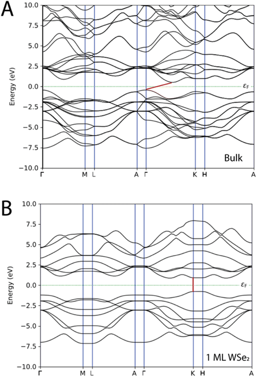 | ||
| Fig. 3 Band structures of WSe2 as (A) a bulk material and as (B) a single layer. The Fermi level is depicted as a dashed green line and the band gap as a red line. | ||
| Wse2 | Bandgap |
|---|---|
| Bulk undoped | 0.94 eV (indirect), 1.58 eV (direct) |
| 1 ML undoped | 1.68 eV (direct) |
| 1.4% of V doping | 0.93 eV |
| 2.8% of V doping | 0.91 eV |
| 5.6% of V doping | 0.85 eV |
| 11.2% of V doping | 0.80 eV |
The projected density of the electronic states (PDOS) shows how the W and Se atoms contribute to both the bands, and only minor differences, in terms of relative intensity and peak position, can be found between the bulk system and the monolayer (Fig. 4). As already reported, the main contribution to both the valence band and the conduction band originates from the d-orbital energy level of W atoms and the p-orbital energy level of Se.3
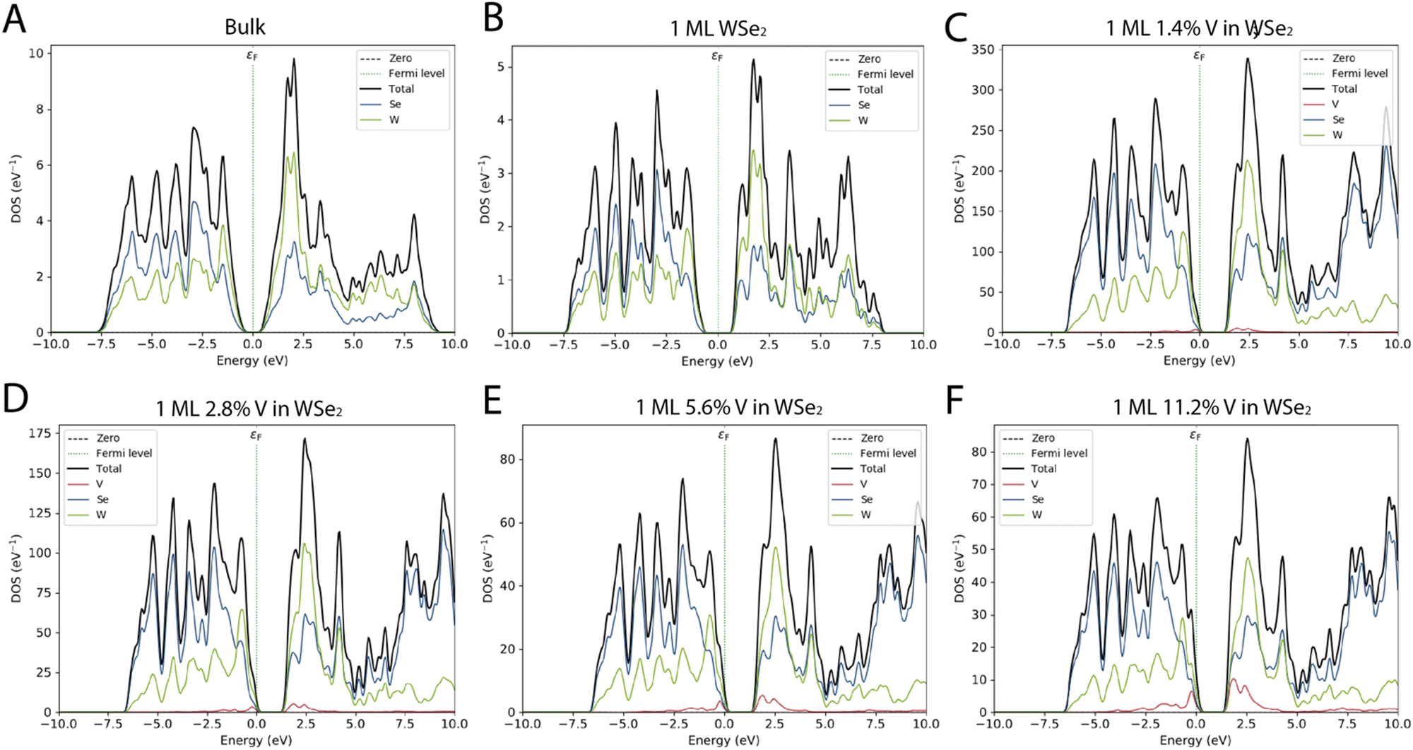 | ||
| Fig. 4 Projected density of the electronic state (PDOS) for WSe2 as a bulk material (A) and 1ML (B). PDOS of WSe2 doped with different percentages of V: WSe2:V 1.4% (C), WSe2:V 2.8% (D), WSe2:V 5.6% (E), and WSe2:V 11.2% (F). The Fermi level is depicted as a dashed green line; the Se, W, and V contributions are reported as blue, green, and red full lines, respectively, while the total DOS is the black line. | ||
The PDOS of the four different systems is based on a ML of WSe2 in which V is replacing 1.4%, 2.8%. 5.6% and 11.2% of the W, showing how even a small percentage of doping affects the behavior of the materials. From Fig. 4 and Table 1, it is possible to notice that when the doping percentage increases, the ML of WSe2:V decreases the bandgap moving from an energy of around 1.6 eV to 0.93 eV. Moreover, because of the introduction of V impurities, the bandgap slightly changed in all the doped systems.
Atomic-scale characterization techniques and density functional theory calculations already reveal that vanadium atoms substitutionally replace tungsten atoms in the WSe2 lattice and introduce multiple defect states that are close to the valence band edge. As it is possible to see from the density of the electronic state in Fig. 4, as the percentage of vanadium gradually increases, there is an enhancement and thus a gradual shift of the valence band close to the Fermi level. When the doping percentage exceeds 2.8%, such effect becomes predominant and confirms the p-type nature of the doping. The VBM shift is even more evident in the higher vanadium inclusion percentage and thus can be attributed to the d orbitals of vanadium. In a more general way, the effect of the vanadium doping brings a total movement of the PDOS, the VBM crosses the Fermi level and such a trend is also matched with the shift of the CBM edge. The p-type nature of the vanadium as dopants is also studied by Kozhakhmetov et al.,16 and confirmed by making use of back-gated field-effect transistors that exhibit an enhanced p-branch (hole) current and a positive threshold shift.
Moreover, the addition of states close to the CBM could be a significant advantage if considering the possibility of the application of these materials for THz interaction, thanks to the low energy amount of these intra-band states.3
Optical properties
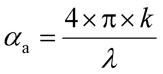
The optical properties of the WSe2 and V doped WSe2 are crucial for the development of a new generation of devices; in this context, of particular interest are the absorption spectra of the material in the visible range of the electromagnetic spectra. Fig. 5 reports the absorption spectra in terms of absorption coefficient (αa) as a function of the wavelength between 250 to 850 nm. The absorption coefficient, also known as the attenuation or extinction coefficient, measures the distributed absorption in a medium per unit length; in other words, it describes the intensity attenuation of the light passing through a material.33 The spectra theoretically predicted show different behavior depending on the number of layers and 1 ML WSe2 has the major absorption peak in the blue region of the visible spectrum (between 390 and 500 nm). In contrast, the bulk WSe2 has a higher value of absorption coefficient in the same region of the electromagnetic spectrum. Still, the peaks are less resolved and the absorption coefficient falls in a quasi-exponential way from the UV to the near IR region.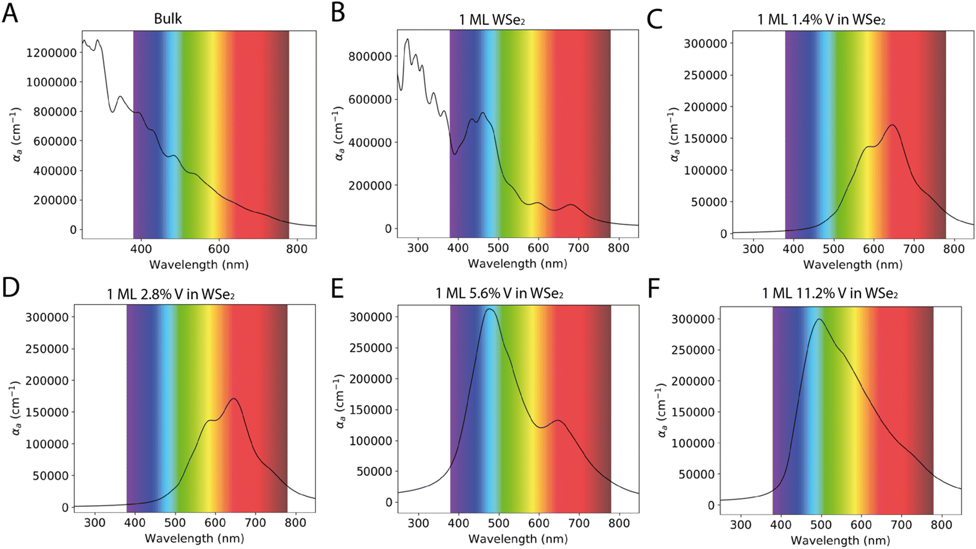 | ||
| Fig. 5 Absorption spectra of WSe2 as a bulk (A) and as 1ML (B). Absorption spectra of WSe2 doped with different percentages of V: WSe2:V 1.4% (C), WSe2:V 2.8% (D), WSe2:V 5.6% (E), and WSe2:V 11.2% (F). The spectra report the absorption coefficient (αa) as a function of the wavelength, between 250 to 850 nm. | ||
The V doping leads to a huge change in the absorption spectrum; when the V percentage does not exceed 2.8%, the optical spectrum shows two major absorption peaks around 590 nm and 750 nm; as a matter of fact, both these transitions were present in the undoped WSe2, but after the incorporation of V, they became prevailing. As the concentration of V is increased, e.g. in the 5.6% WSe2:V, another transition became preponderant, and this is situated between 400–550 nm; actually, the same transition was also present in the 1 ML WSe2. A second band less resolved and less intense is still detected around 750 nm, similar to the one present in the spectra of 1.4% and 2.8% WSe2:V. The system containing V doping at 11.2% shows a single transition centered around 500 nm characterized by a broadening and a low resolution of the other bands.
As reported in the literature, the presence of V brings an enhancement in Raman defect modes and quenching of WSe2 photoluminescence.16 These authors showed that the photoluminescence spectra exhibit a similar dopant concentration dependence: intrinsic WSe2 displays a 1.65 eV optical band gap, while is redshifted by 40 and 80 meV when there is 0.6% V:WSe2 and 1.1% V:WSe2, respectively, with reduced global photoluminescence intensity. As the dopant concentration increases to 1.9%, there is a complete quenching in the photoluminescence. These results are in line with the hypothesis according to which V is expected to be a p-type dopant in WSe2 and donates an extra hole to the system. The dopant impurities result in non-radiative recombination that alters the photoluminescence by quenching the intensity for vanadium doping concentrations over 1.9%.16,34
To confirm the ability of the DFT methodology proposed herein to describe the peculiarities of both undoped and V-doped WSe2, further evaluation has been carried out in terms of (i) the real part (Re[ε]) of the dielectric function (Fig. 6), which describes the ability of the matter to interact with an electric field without absorbing energy, (ii) the imaginary part (Im[ε]) of the dielectric function (Fig. 6), which describes the ability of the matter to permanently absorb energy from a time-varying electric field, (iii) the extinction coefficient (Fig. S2 of the ESI†), which represents the capability of the matter to absorb light, and (iv) the refractive index (Fig. S3 of the ESI†), which is useful to understand the ability of the matter to bend or refract the light that passes through the material itself; the spectra have been reported as a function of the energy of the electric field expressed in eV.
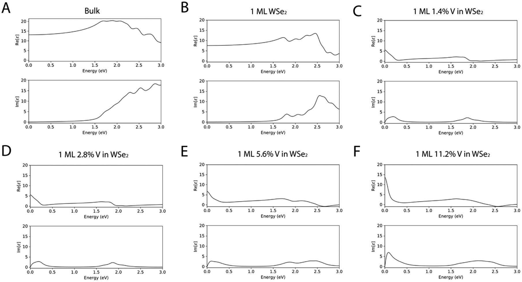 | ||
| Fig. 6 Real (Re[ε]) and imaginary (Im[ε]) function of the dielectric constant of WSe2 as a bulk material (A) and as 1 ML (B). Dielectric functions of WSe2 doped with different percentages of V: WSe2:V 1.4% (C), WSe2:V 2.8% (D), WSe2:V 5.6% (E), and WSe2:V 11.2% (F). The dielectric values are reported as functions of the energy between 0 and 3 eV. | ||
As it is possible to see from the dielectric functions, both the undoped systems have a similar trend in terms of shapes of the spectral features, but the values of both the real and imaginary dielectric functions are higher in the bulk WSe2. The trend of the spectra of the doped systems differ from the undoped one, but the systems are very similar in shape between the different percentages of V doping, with an increased intensity in the ε spectra as the percentage of V became bigger.
Method
A quantum ATK atomic-scale modeling platform has been used to model all the WSe2 structures and to perform all calculations.26–28 During the optimization of the geometries and for the calculation of the optical and electronic properties, the electron basis has been expanded in linear combination using the atomic orbital (LCAO) method for Se, W, and V entities resembling the SIESTA formalism.35 All simulations have been carried out using the Perdew–Burke–Ernzerhof (PBE) generalized gradient approximation (GGA) density functional for the electron xc energy.36 The Hybrid HSE06 functional was used to calculate the band gap energies and the band structures reported in the ESI† (Table S1 and Fig. S1). For each atom, the ionic cores have been represented by norm-conserving (NC) PseudoDojo (PDj) pseudopotentials.37 The corrective Grimme DFT-D3 term has been added to better consider the van der Waals interactions, and periodic boundary conditions (PBCs) have been used along all axes for the bulk system, while PBCs have been applied only to the a and b axes to estimate the properties of the layered structures; in this way, it is possible to avoid problems with boundary effects caused by the finite size and to reduce the calculation time while maintaining high accuracy. The energy cut-off has been fixed at 1200 eV and the Brillouin-zone integration has been performed over a 15 × 15 × 15 k-points grid. These parameters assure the total energy convergence of 5.0 × 10⁻⁶ eV per atom, the maximum stress of 2.0 × 10⁻² GPa, and the maximum displacement of 5.0 × 10⁻⁴ Å.The optical properties have been determined by two components of the dielectric function ε(ω) = εr(ω) + iεi(ω). The imaginary part εi(ω) of the dielectric constant can be determined from eqn (1):38
 | (1) |
The real part of the dielectric constant can be obtained with the following eqn (2):
 | (2) |
| εr(ω) = n2 − k2 | (3) |
| εi(ω) = 2nk | (4) |
 | (5) |
Conclusions
Tungsten diselenide WSe2 belongs to the 2D TMDs characterized by unique structural, optical, and electronic properties. As a member of the TMD family, WSe2 displays interesting features, making it a promising material for a wide range of applications, including optoelectronics, energy storage, and THz communications. In this paper, we presented an ab initio calculation making use of density functional theory (DFT), by using PBE-GGA for the xc energy, the PseudoDojo pseudopotential, and the corrective Grimme DFT-D3 term to consider the van der Waals interactions. The study is based on the properties of bulk and monolayer WSe2; in particular, the band structures of WSe2 undergo an indirect-to-direct gap when weakened to a single monolayer, while only minor differences were found between the bulk and monolayer in terms of PDOS and absorption spectra.Then, four different systems based on vanadium doped-WSe2 were investigated from the optical and electronic points of view. The systems contain different percentages of V: (i) WSe2:V 1.4%, (ii) WSe2:V 2.8%, (iii) WSe2:V 5.6%, and (iv) WSe2:V 11.2%.
The doping percentage is calculated considering the number of V atoms (replacing W) and the total number of W atoms in the unit cell. Vanadium doping brings a reduction of the bandgap and a global shift of the projected density of states, the VBM crosses the Fermi level, and such a trend matches with the p-type nature of the vanadium. Moreover, the presence of vanadium also affected the absorption spectra of the systems; the electronic transition led to a band shift and broadening and changed in terms of relative intensity, as the percentage of vanadium changes. Moreover, we studied the real and the imaginary dielectric functions, the extinction coefficient, and the refractive index, to understand the capability of these materials to interact with an applied electric field. These properties showed a similar trend for two undoped systems that differ from the V-doped ones. Meanwhile, the different percentages of V affected the optical features mostly in terms of intensity.
Author contributions
Conceptualization, E. P.; methodology, E. P. and E. M.; validation, E. P., E. M.; investigation, E. P.; data curation, E. P.; writing – original draft preparation, E. P.; writing – review and editing, E. P., E. M., P. L. S., L. P. and D. M; visualization, E. P.; supervision, P. L. S.; project administration, E. P., E. L., P. L. S., L. P. and D. M. All authors have read and agreed to the published version of the manuscript.Conflicts of interest
There are no conflicts to declare.Acknowledgements
This work has been supported by the European Union HORIZON-EIC, 2022, project number 101099552, “Nano-scale Development of Plasmonic Amplifiers Based on 2D Materials” (PLASNANO).References
- A. Y. Pawar, D. D. Sonawane, K. B. Erande and D. V. Derle, Drug Invent. Today, 2015, 5, 157–163 CrossRef.
- C. J. Docherty, P. Parkinson, H. J. Joyce, M. H. Chiu, C. H. Chen, M. Y. Lee, L. J. Li, L. M. Herz and M. B. Johnston, ACS Nano, 2014, 8, 11147–11153 CrossRef CAS.
- K. Si, Y. Huang, Q. Zhao, L. Zhu, L. Zhang, Z. Yao and X. Xu, Appl. Surf. Sci., 2018, 448, 416–423 CrossRef CAS.
- W. T. Hsu, L. S. Lu, D. Wang, J. K. Huang, M. Y. Li, T. R. Chang, Y. C. Chou, Z. Y. Juang, H. T. Jeng, L. J. Li and W. H. Chang, Nat. Commun., 2017, 8, 1–7 CrossRef CAS.
- M. Tahir, Phys. E, 2018, 97, 184–190 CrossRef.
- H. Liu, P. Lazzaroni and C. Di Valentin, Nanomaterials, 2018, 8, 1–17 Search PubMed.
- D. Muoi, N. N. Hieu, H. T. T. Phung, H. V. Phuc, B. Amin, B. D. Hoi, N. V. Hieu, L. C. Nhan, C. V. Nguyen and P. T. T. Le, Chem. Phys., 2019, 519, 69–73 CrossRef.
- A. Eftekhari, J. Mater. Chem. A, 2017, 5, 18299–18325 RSC.
- W. J. Schutte, J. L. De Boer and F. Jellinek, J. Solid State Chem., 1987, 70, 207–209 CrossRef.
- E. Pavoni, M. G. Modreanu, E. Mohebbi, D. Mencarelli, P. Stipa, E. Laudadio and L. Pierantoni, Nanomaterials, 2023, 13, 1319 CrossRef PubMed.
- E. Pavoni, E. Bandini, M. Benaglia, J. K. Molloy, G. Bergamini, P. Ceroni and N. Armaroli, Polym. Chem., 2014, 5, 6148–6150 RSC.
- Y. Ma, B. Liu, A. Zhang, L. Chen, M. Fathi, C. Shen, A. N. Abbas, M. Ge, M. Mecklenburg and C. Zhou, ACS Nano, 2015, 9, 7383–7391 CrossRef CAS PubMed.
- A. Falin, M. Holwill, H. Lv, W. Gan, J. Cheng, R. Zhang, D. Qian, M. R. Barnett, E. J. G. Santos, K. S. Novoselov, T. Tao, X. Wu and L. H. Li, ACS Nano, 2021, 15, 2600–2610 CrossRef CAS PubMed.
- Y. Ding, Y. Wang, J. Ni, L. Shi, S. Shi and W. Tang, Phys. B, 2011, 406, 2254–2260 CrossRef CAS.
- J. H. Park, A. Rai, J. Hwang, C. Zhang, I. Kwak, S. F. Wolf, S. Vishwanath, X. Liu, M. Dobrowolska, J. Furdyna, H. G. Xing, K. Cho, S. K. Banerjee and A. C. Kummel, ACS Nano, 2019, 13, 7545–7555 CrossRef CAS.
- A. Kozhakhmetov, S. Stolz, A. M. Z. Tan, R. Pendurthi, S. Bachu, F. Turker, N. Alem, J. Kachian, S. Das, R. G. Hennig, O. Gröning, B. Schuler and J. A. Robinson, Adv. Funct. Mater., 2021, 31, 2105252 CrossRef CAS.
- H. Terrones, F. López-Urías and M. Terrones, Sci. Rep., 2013, 3, 234–243 Search PubMed.
- A. V. Gorbatova, D. I. Khusyainov and A. M. Buryakov, Tech. Phys. Lett., 2019, 45, 1262–1265 CrossRef CAS.
- K. Cen, S. Yan, N. Yang, X. Dong, L. Xie, M. Long and T. Chen, Vacuum, 2023, 212, 112020 CrossRef CAS.
- H. Li, L. Xu, X. Huang, J. Ou-Yang, M. Chen, Y. Zhang, S. Tang, K. Dong and L. L. Wang, Int. J. Hydrogen Energy, 2023, 48, 2186–2199 CrossRef CAS.
- J. Zeng, L. Xu, X. Luo, T. Chen, S. H. Tang, X. Huang and L. L. Wang, Tungsten, 2022, 4, 52–59 CrossRef.
- L. Ju, Y. Dai, W. Wei, M. Li and B. Huang, Appl. Surf. Sci., 2018, 434, 365–374 CrossRef CAS.
- P. Mallet, F. Chiapello, H. Okuno, H. Boukari, M. Jamet and J. Y. Veuillen, Phys. Rev. Lett., 2020, 125, 036802 CrossRef CAS PubMed.
- S. J. Yun, D. L. Duong, D. M. Ha, K. Singh, T. L. Phan, W. Choi, Y. M. Kim and Y. H. Lee, Adv. Sci., 2020, 7, 1–14 Search PubMed.
- X. Dong, H. Li, T. Chen, L. Xu and G. Zhou, Mater. Sci. Semicond. Process., 2022, 143, 106537 CrossRef CAS.
- S. Smidstrup, T. Markussen, P. Vancraeyveld, J. Wellendorff, J. Schneider, T. Gunst, B. Verstichel, D. Stradi, P. A. Khomyakov, U. G. Vej-Hansen, M.-E. Lee, S. T. Chill, F. Rasmussen, G. Penazzi, F. Corsetti, A. Ojanperä, K. Jensen, M. L. N. Palsgaard, U. Martinez, A. Blom, M. Brandbyge and K. Stokbro, J. Phys.: Condens. Matter, 2019, 32, 015901 CrossRef PubMed.
- E. Pavoni, E. Mohebbi, D. Mencarelli, P. Stipa, E. Laudadio and L. Pierantoni, Nanomaterials, 2022, 12, 1–12 CrossRef.
- E. Pavoni, E. Mohebbi, P. Stipa, D. Mencarelli, L. Pierantoni and E. Laudadio, Materials, 2022, 15, 4175–4188 CrossRef.
- D. Voß, P. Krüger, A. Mazur and J. Pollmann, Phys. Rev. B: Condens. Matter Mater. Phys., 1999, 60, 14311–14317 CrossRef.
- W. J. Schutte, J. L. De Boer and F. Jellinek, J. Solid State Chem., 1987, 70, 207–209 CrossRef.
- D. L. Duong, S. G. Kim and Y. H. Lee, AIP Adv., 2020, 10, 065220 CrossRef.
- W. Zhao, R. M. Ribeiro, M. Toh, A. Carvalho, C. Kloc, A. H. Castro Neto and G. Eda, Nano Lett., 2013, 13, 5627–5634 CrossRef.
- J. Gong and S. Krishnan, Dye-Sensitized Solar Cells: Mathematical Modelling, and Materials Design and Optimization, 2019, pp. 51–81 Search PubMed.
- D. H. Lien, S. Z. Uddin, M. Yeh, M. Amani, H. Kim, J. W. Ager, E. Yablonovitch and A. Javey, Science, 2019,(364), 468–471 CrossRef PubMed.
- J. M. Soler, E. Artacho, J. D. Gale, A. García, J. Junquera, P. Ordejón and D. Sánchez-Portal, The SIESTA method for ab initio order-N materials simulation, J. Phys.: Condens. Matter, 2002, 14, 2745 CrossRef CAS.
- J. P. Perdew, K. Burke and M. Ernzerhof, Generalized Gradient Approximation Made Simple, Phys. Rev. Lett., 1996, 77, 3865 CrossRef CAS.
- M. J. van Setten, M. Giantomassi, E. Bousquet, M. J. Verstraete, D. R. Hamann, X. Gonze and G.-M. Rignanese, Comput. Phys. Commun., 2018, 226, 39–54 CrossRef CAS.
- B. Mortazavi, M. Shahrokhi, M. Makaremi and T. Rabczuk, Nanotechnology, 2017, 28, 115705 CrossRef PubMed.
Footnote |
| † Electronic supplementary information (ESI) available. See DOI: https://doi.org/10.1039/d3ma00940h |
| This journal is © The Royal Society of Chemistry 2024 |