
 Open Access Article
 This Open Access Article is licensed under a Creative Commons Attribution-Non Commercial 3.0 Unported Licence
A robust and high performance copper silicide catalyst for electrochemical CO2 reduction†
Vladislav
Dřínek
 *a,
Pavel
Dytrych
a,
Radek
Fajgar
a,
Mariana
Klementová
b,
Jaroslav
Kupčík
a,
Jaromír
Kopeček
b,
Petr
Svora
b,
Martin
Koštejn
a,
Věra
Jandová
a,
Karel
Soukup
a and
Radim
Beranek
c
*a,
Pavel
Dytrych
a,
Radek
Fajgar
a,
Mariana
Klementová
b,
Jaroslav
Kupčík
a,
Jaromír
Kopeček
b,
Petr
Svora
b,
Martin
Koštejn
a,
Věra
Jandová
a,
Karel
Soukup
a and
Radim
Beranek
c
aInstitute of Chemical Process Fundamentals of the CAS, v.v.i., Rozvojová 135, 16500 Prague, Czech Republic. E-mail: drinek@icpf.cas.cz
bInstitute of Physics of the CAS, v.v.i., Na Slovance 2, 18200 Prague, Czech Republic
cInstitute of Electrochemistry, Ulm University, Albert-Einstein-Allee 47, 89081 Ulm, Germany
First published on 19th February 2024
Abstract
A copper-based catalyst CuxSi (3 < x < 5) was prepared using chemical vapor deposition (CVD) of butylsilane (BuSiH3) on copper substrates. By varying the precursor flow, we obtained two catalyst variants, one with and one without a SiCx shell. Both variants exhibited large specific areas, owing to the presence of grown nanostructures such as nanoplatelets, nanowires, nanoribbons, and microwires. Remarkably, the catalytic performance of both variants remained stable even after 720 hours of continuous operation. The porous and thick catalyst layer (over a hundred micrometers) on the substrate significantly increased the residence time of intermediates during the electrochemical CO2 reduction reactions (eCO2RR). We observed a high selectivity towards ethanol (∼79%) in neutral CO2-saturated electrolytes and a high selectivity towards acetic acid (∼72%) in alkaline electrolytes. Importantly, the ratio between generated ethanol and acetate could be shifted by adjusting the pH and applied potential. This work thus establishes copper silicides as robust and promising electrocatalysts for selective CO2 conversion to high-value multi-carbon products.
Introduction
According to the IPCC (Intergovernmental Panel on Climate Change), carbon dioxide (CO2) is the primary greenhouse gas responsible for global warming and climate change. Its sixth assessment report (AR6) declares that if CO2 concentrations in the atmosphere triple by 2075, average temperatures will rise by up to 4.4 °C. Therefore, political decisions taking those assumptions into account make efforts to curb the CO2 rise in atmosphere through economic-administrative restrictions introducing, for example, the forced closing of coal power stations, the pushing of electromobility and the support of passive civil engineering. However, given the challenge of replacing significant CO2 emitters (especially large stationary sources) overnight, viable alternatives are needed. A possible alternative is carbon capture and storage (CCS) technology, whereby CO2 is captured either at the CO2 source outputs or directly from the air and then fixed in a matter (such as minerals or water) and pumped into the earth.1 Yet, perhaps an even more compelling approach is to leverage CO2 as a valuable feedstock for chemical synthesis within circular conversion processes, effectively creating closed-loop systems that generate zero net emissions.Electrochemical CO2 reduction reactions (eCO2RR) can be employed to synthesize a diverse array of hydrocarbons and other reduced products.2–5 Such production typically requires sophisticated electrochemical cells equipped with advanced catalytic materials. Promising results have been achieved using carbon-supported metals, with notable successes in CO and HCOOH production observed with gold and silver, and with tin, bismuth, indium, and their oxides, respectively. Copper or copper-based oxides or alloys are the preferred catalytic electrode materials for generating C2+ hydrocarbons, owing to their ability to promote the formation of carbonaceous chains.4,5 Several studies have examined the influence of copper oxidation states and substrates on eCO2RR effectiveness, specifically with regard to C2+ product formation.6,7 For example, copper, in its most active state with respect to C2+ product formation, was reported to possess a partial charge close to +I with a faradaic efficiency (FE) for C2+ > 75% under optimized electrochemical, hydrodynamical and mass transport conditions.7 Another parameter that determines the eCO2RR selectivity is the size and accessibility of catalytic spots in the copper-based materials.8 Last but not least, the mutual proximity of catalytic active sites and modus operandi (e.g., potentiostatic vs. galvanostatic, current density, pH, etc.) plays a critical role.9,10 The lack of CO2 in catalytic active sites of electrocatalysts leads to an increase in parasitic side reactions, especially the hydrogen evolution reaction (HER).11
CuxSi is an alloy that only forms copper-rich phases ranging from ∼70 to 90 at% Cu.12 This phase region is vastly complex. The most silicon-containing phase is Cu3Si (also denoted as Cu76Si24, Cu3+xSi and Cu3Si1−x) with 23–25 at% Si content. With increasing temperature, the structure this phase changes slightly (η′′′ → η′′ → η′ → η3 → η2 → η1).13,14 All these phases can be indexed with a similar basic unit cell (trigonal a = 4.08 Å, c = 7.36 Å), although each phase differs in modulation.
CuxSi alloys were studied earlier in microelectronics enabling the reduction of atom migration from copper interconnects. Nevertheless, even in relation to silicides, the problem of Cu migration persists. Therefore, the addition of heteroatoms or novel alloys has been studied.15,16 Copper silicides have been studied as negative electrodes in Li-ion batteries17,18 due to their high electrical conductivity, whereby, for example, ternary lithium-rich silicides Li7CuSi2 and Li7.3CuSi3 were identified as suitable candidates.19
Copper-based silicide nanostructures, such as nanowires, nanorods, and nanotubes, have been synthesized and tested for their use in battery applications. The robustness of the nanostructures was demonstrated by the volume expansion of Si nanowires due to lithiation without any obvious surface cracking.20 The nanostructures have demonstrated good adhesion and stability during cycling, and various synthesis methods have been explored.21–24 Copper silicide nanostructures also have potential applications in microelectronic devices.25–29
Finally, copper is a widely used catalyst, either pristine or as an alloy with other elements. In the case of copper silicide, the most known catalyst application is the so-called the Direct (Müller–Rochow) process.30,31 In this process, chloromethane CH3Cl is converted mostly into dichlorodimethylsilane (CH3)2SiCl2 and other chloroorganosilanes. Several million tons of (CH3)2SiCl2 are synthetized each year for their use in the production of siloxanes, among other things.
Copper-containing silicides and germanides have been prepared and studied for over a decade.32–36 Several sorts of nanostructured objects have been synthetized, described and analyzed to investigate the possible influence of nanodimensions on the structure of the objects. For example, an incommensurately modulated structure was identified in Cu3(SiGe) nanoplatelets,33 and a novel Cu3Si(η′′′) phase was discovered.14 Under varying precursors and experimental conditions, plenty of morphologies, including nanoobjects were observed in a CuxSi material.34
The choice of copper silicide alloys for eCO2RR is motivated by several reasons: (i) copper or copper-based materials have demonstrated the best catalytic properties with respect to formation of C2+ products, (ii) copper silicide phases are rich in copper, (iii) copper and silicon are non-toxic, easily processed, cheap and available, especially compared to expensive catalytic elements (Au, Ag, Pt, Pd, Ir), and (iv) we have already gathered vast knowledge about silicon-based materials and their preparation in nanostructured forms. Herein, we report the fabrication and detailed characterization of nanostructured CuxSi catalysts with large specific surface areas and their electrochemical performance in eCO2RR. Most notably, we find that the CuxSi catalyst is highly selective for C2+ products, and the high selectivity towards the main product ethanol (∼79%) vs. acetate (∼72%) is controllable by pH (neutral vs. alkaline) solution. As the catalyst can be operated without any deterioration for more than 720 h, our work establishes copper silicides as robust and promising electrocatalyts for selective CO2 conversion to high-value products.
Experimental
A CuxSi based catalyst deposit was prepared using the CVD approach (Fig. S1, ESI†). First, a copper sheet (Provetro, 99.99%) of particular dimensions of 40–60 mm × 12 mm × 0.1/0.5 mm (length × width × thickness) was ground by a piece of sandpaper No. 1200, cleaned in an ultrasonic bath with acetone (Lachner, 99.98%) and quickly dried using a heat gun. Afterwards, the sheet was inserted into a quartz tube with an inner diameter of 14 mm and put into an 018LP model oven (Elektrické pece Svoboda). Vacuum was established by means of a turbostation (HiPace 10, Pfeiffer Vacuum) at 10−4–10−3 Pa for several hours. After reaching the final temperature of 500 (570) °C with a ramp rate of 8 °C min−1, the turbostation was switched off. The precursor, butylsilane BuSiH3, Bu = C4H9 (Sigma-Aldrich, ≥97%), was introduced until the target pressure was reached. At that moment, a precise dosing valve (EVN 116, Pfeiffer Vacuum) was opened to control the pumping speed of the rotary pump. The vapor mass flow from the ampoule with the precursor to the quartz tube was maintained by another precise dosing valve at a desired flow during the whole experiment run, which lasted approximately 230–300 and 620 min for the samples prepared on the copper substrates of 0.1 and 0.5 mm thickness, respectively. The deposit was removed from the tube for further analyses after natural cooling to room temperature.Nitrogen physisorption measurements at cryogenic conditions (77.35 K) were performed by the automated volumetric gas adsorption analyzers ASAP 2020 and ASAP 2050 (Micromeritics). To guarantee the accuracy of the obtained adsorption isotherms, high purity nitrogen (grade of 99.9995 vol%) as well as helium (grade of 99.9995 vol%; used for determination of the free-space volume typically performed prior to analysis) were used. The specific surface area, S (BET), was calculated from the nitrogen adsorption isotherm in the relative pressure range corresponding to p/p0 = 0.05–0.25, using the standard Brunauer–Emmett–Teller (BET) procedure.
Several scanning electron microscopes were used for morphology and microstructure characterization of the samples. The initial observations were carried out at a scanning electron microscope (Indusem, Tescan) equipped with an energy-dispersive analyzer unit (Quantax 200, Bruker) and a semiconductor SDD detector with working resolution better than 125 eV (XFlash 5010, Bruker). The gathering and evaluation of EDX data were performed using Esprit 1.9 microanalysis software. SEM images were taken within the acceleration voltage span of 15–30 kV. Samples that underwent SEM analyses of cross-section morphology and composition were fixed using carbon tape (Spi Supplies). A more detailed imaging of the surface was performed using a SEM (Quanta 3D, FEI) operated at 5 kV, a working distance of 10 mm, and currents ranging from 8 to 30 pA. For preparation and characterization of the samples in the cross-section, a FIB-SEM (FERA 3, Tescan) was used. The microscope was equipped with a xenon plasma FIB. The cross-cuts were performed using a silicon protective mask to minimize curtaining artefacts on the cross-cut area. To analyze the samples, coupled EDAX analyzers were used (EDS Octane Super 60 mm2 and EBSD DigiView V).
Transmission electron microscopy (TEM) was used for detailed characterization of individual nanoobjects. The data were acquired on a TEM (Tecnai TF20, FEI) operated at 200 kV (FEG, 1.9 Å point resolution) with an EDAX Energy Dispersive X-ray (EDX) detector attached. The images were recorded on a Gatan CCD camera with a resolution of 2048 × 2048 pixels using the Digital Micrograph software package. The EDX spectra were evaluated using the FEI TIA software.
The structural characterization of the nanoobjects was performed by electron diffraction (3D ED). The data were collected on a TEM (Tecnai G2 20, FEI) operated at 200 kV with a LaB6 cathode, equipped with an ASI Cheetah direct detection camera (512 × 512 pixels), using the step-wise approach (tilt range ±50 deg, step 0.5 deg). The data were processed in the PETS 2.0 software. The samples for TEM were prepared on holey-carbon coated Au grids by brushing the grid against the substrate containing the deposit.
The powder X-ray Diffraction (pXRD) measurement was performed using a Bruker D8 Advance Eco diffractometer (Bruker AXS GmbH) working with Cu Kα radiation (λ = 1.54056 Å) and equipped with a silicon-strip LynxEye detector with an energy resolution that allowed fluorescence and Kβ radiation to be eliminated. The sample was rotated at a speed of 6 rpm during measurements. Data were collected in the 2θ range of 10–80° with a step size of 0.02 and 10 s time per step. The phase identification was performed with the Diffrac.Eva software v5.1.0.5 which contains the PDF2 database (2019 release).
The surface analysis of the samples, determining the composition and chemical state of the elements from their surfaces, was inspected by X-ray photoelectron spectroscopy. Kratos ESCA 3400 furnished with a polychromatic Mg X-ray source of Mg Kα radiation (energy: 1253.4 eV) was used. The base pressure was kept at 5.0 × 10⁻⁷ Pa during the analysis. The spectra were taken over the Cu 2p, O 1s, C 1s, and Si 2p regions with 0.05 eV steps, and survey spectra were measured in the region of 0–1000 eV with a 0.2 eV step. The spectra were measured with a pass energy of 25 eV. The spectra were fitted using a Gaussian–Lorentzian line shape (GL30) after Shirley background subtraction, and a damped non-linear least squares routine was used to separate the chemically shifted states. The samples were sputtered with Ar+ ions at 1 kV with a current of 10 μA for 90 and 180 s to remove the superficial layers. The spectra were calibrated to the C 1s line, centering at 284.8 eV.
The electrochemical measurements were performed in a home-designed H-cell with either a proton exchange membrane or no membrane and Pt as an anode (Fig. S2, ESI†). The electrolysis was controlled by an Autolab (Autolab Multi 204) potentiostat. Saturated 3.5 M Ag/AgCl was used as the reference electrode. The RHE was calculated from the applied potential using eqn (1):
| E(RHE) = E(Ag/AgCl) + 0.203 + 0.0592pH | (1) |
All electrocatalytic reactions were conducted at ambient pressure and temperature. 0.1 M potassium carbonate (K2CO3) solution was typically used as the electrolyte. High-purity CO2 (99.995%, Linde) was supplied to the electrolyte at a constant rate with a constant flow rate monitored by a mass flow controller. Unless otherwise stated, the reaction was conducted in 0.1 M KOH with a flow rate of ca 50 mL min−1 STP for 30 min followed by 10 mL min−1 STP. During the electrolytic reaction, the effluent gas from the cathodic compartment went through the sampling syringe, was analyzed in an on-site build quadruple mass spectrometer (m/z = 1–200). The liquid products (formate, acetate, ethanol, propan-1-ol etc.) were analyzed by 1H NMR spectroscopy. The liquid products were collected and analyzed after 36 hours of electrolysis.
The mass spectra of the gas mixtures were measured using a spectrometer Quadruvac Q 200 (Leybold–Heraeus) in the m/z range 1–200 (Fig. S3, ESI†). The samples were injected into the cell equipped with a membrane vacuum gauge Barocell 100MB (Edwards). The cell was connected to a mass spectrometer inlet through a capillary with an internal diameter of 0.20 mm. The mass spectra were recorded by Oscilloscope DS8102 (Owon).
All NMR spectra were measured on a Varian UNITY INOVA 500 MHz NMR spectrometer with a 5 mm indirect detection pulse field gradient probe. 0.5 mL of water solution with the reaction products (electrolyte) and 0.2 mL of deuterium oxide D2O were filled into a 5 mm glass NMR sample tube. The D2O solvent contained 0.8 mM of sodium salt of trimethylsilyl-[2,2,3,3-d4]-propionic acid (TSP), which was used as a reference standard (δ = −0.016 ppm) and to estimate reaction products amounts. All samples were measured with 1D NOESY sequence with a relaxation delay of 15 s, saturation delay of 2 s, acquisition of 2.7 s (i.e. scan repetition time of 19.7 s), saturation power of 80 ± 2 Hz, and a 90-degree pulse length of about 5 μs. 1024 scans were collected for each sample. The pulse widths were calibrated before the measurement of each sample, and the transmitter offset for the best solvent suppression was always checked as well. The mix delay was kept at 10 ms for each sample.
Results and discussion
Two types of copper silicide deposits were prepared by changing the single experimental parameter, precursor mass flow. They are named according to their macroscopic color as bluish and gray-black.The energy dispersive X-ray analysis (EDX) on the bluish deposit revealed an overall elemental composition of [Cu]![[thin space (1/6-em)]](https://www.rsc.org/images/entities/char_2009.gif) :[Si]:[O]:[C] = 48:27:2:23, providing the ratio [Cu]:[Si] = 1.8. A higher copper concentration was found for the gray-black deposit, with [Cu]:[Si]:[O]:[C] = 63:17:2:18 and, [Cu]:[Si] = 3.7. Although the macroscopic morphology varied from sample to sample, the elemental and structural compositions were similar for both the bluish and gray-black variants (see below). The samples prepared on ∼0.1 mm thick copper substrates became fragile and could be broken apart to expose the cross-section of the grown samples.
:[Si]:[O]:[C] = 48:27:2:23, providing the ratio [Cu]:[Si] = 1.8. A higher copper concentration was found for the gray-black deposit, with [Cu]:[Si]:[O]:[C] = 63:17:2:18 and, [Cu]:[Si] = 3.7. Although the macroscopic morphology varied from sample to sample, the elemental and structural compositions were similar for both the bluish and gray-black variants (see below). The samples prepared on ∼0.1 mm thick copper substrates became fragile and could be broken apart to expose the cross-section of the grown samples.
According to powder X-ray Diffraction (pXRD), only two dominant crystallographic phases were distinguished (Fig. 1): cubic Cu15Si4(ε)37 and trigonal Cu3+xSi(η′′′).14 The bluish sample contained a significantly lower amount of the ε-phase (about 20 wt%) than the gray-black sample (about 45 wt%), which is demonstrated in line with the difference in their surface and microscopic structure (Fig. 2).
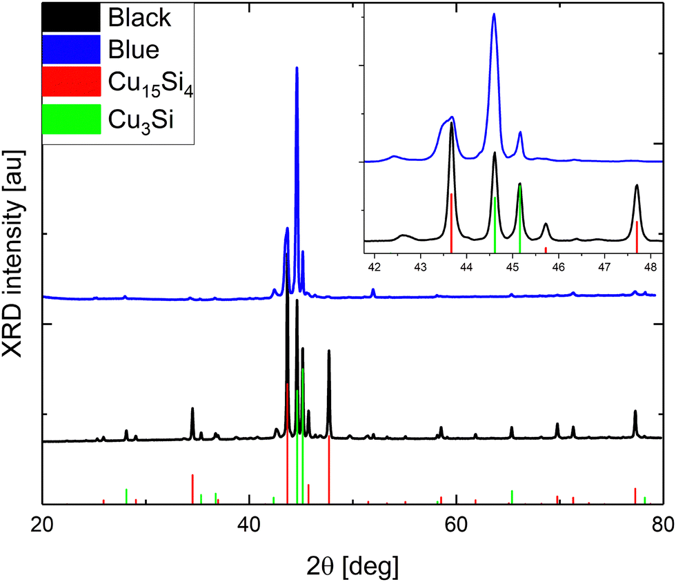 | ||
| Fig. 1 pXRD analyses of the bluish and gray-black samples. The inset visualizes the overlapping peaks in the range of 42°–48° in detail. | ||
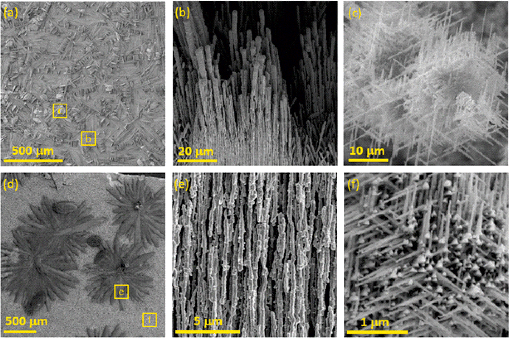 | ||
| Fig. 2 SEM observations of the bluish sample on the top (a)–(c) and gray-black sample at the bottom (d)–(f). The yellow squares with a letter inside correspond to the nanostructures depicted in the images with the same letter. | ||
The bluish sample contained microwires (MWs) with flat interwoven nanoribbons (NRBs) (Fig. 2c) growing perpendicular to MWs (Fig. 2b). MWs were one to five microns in diameter and hundreds of microns in length. Some of the MWs lay on the surface, while others protruded. The same phenomenon had been observed previously and described as “holey” nanoplatelets consisting of flat nanoribbons of Cu3Si.34 On the surface of the gray-black sample, large, up to one-millimeter, black, flower-like aggregates were present on top of the silver-gray background as seen in SEM (Fig. 2d) and more detailed FESEM images (Fig. S4, ESI†). The black aggregates were composed of nanorods (NRs) about 200 to 300 nm in diameter with lengths of several microns similar to the NRBs in the bluish sample (Fig. 2e). The background was composed of nanoneedles (NNs) with diameters ranging from 50 to 100 nm (Fig. 2f). These NNs formed a thick porous network that was interconnected at a 120 deg angle. The Cu15Si4(ε) phase is most likely responsible for the formation of NNs, whereas the other objects are most likely related to the Cu3Si(η′′′) phase.
The scanning electron microscopy (SEM) cross-section view demonstrates the vertical structure of the deposit (Fig. 3 and Fig. S5, S6, ESI†). Individual objects (region 1) are visible on the surface gradually passing into thick, porous sponge-like matter (region 2). In the middle, the partially decomposed remains of the original copper substrate (region 3) are evident. Between the rest of the copper substrate and the formed porous CuxSi matter, large, microscopic cracks (region 4) formed due to the structural interlayer stress between the copper and the CuxSi phase. The cracks separate the original Cu substrate which has also undergone structural changes during the deposition process. The EDX analysis of the rest of the copper substrate revealed some amount of silicon (Fig. 3), and therefore confirmed the overall transformation of the original copper substrate into a CuxSi catalyst. The combined thickness of the catalyst regions on both sides, where the electrochemical reaction takes place, is approximately 180 μm (Fig. S6, ESI†).
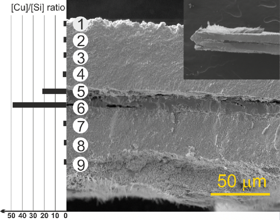 | ||
| Fig. 3 SEM image of the cross-section of the bluish deposit (Cu substrate 0.1 mm). Individual EDX spots 1 → 9 are indicated in the image and [Cu]/[Si] atomic ratios are depicted. The investigated deposit is shown inset in the upper right corner, clinging to a carbon tape by its edge. | ||
In order to obtain a bare cross-section in a standardized manner, a focused ion beam (FIB) procedure was performed on the gray-black sample (Fig. S7, ESI†) for comparison. While the cross-sectional view obtained through this method may not capture all details, it does reveal a discernible pattern of specific regions in the EDX elemental maps of copper and silicon (Fig. S7d and e, ESI†), albeit somewhat indistinctly. The elemental maps show very little variation, probably caused by the very close chemical composition of both phases (77% Cu(η′′′), 78.5% Cu(ε))38 as well as by the porous character of the sample that influenced the accuracy of the measurement. The formation of similar structures was also previously observed during the annealing of a-Si(50 nm)/Cu(200 nm)/a-Si(50 nm). Mutual diffusion and mixing of Si and Cu atoms resulted in a layered structure that was homogeneous in terms of elemental composition but different in morphology.39
We succeeded in obtaining even thicker CuxSi catalyst layers in order to increase the residence time of the intermediates inside the catalyst. This was achieved by running longer experiments (up to 620 min), increasing the temperature to 570 °C and using a 0.5 mm thick copper substrate (Fig. S8, ESI†). The bulk deposit grown was compact yet not as fragile as the deposits prepared on substrates of 0.1 mm thickness. It was impossible to break it apart without any distortion and/or deformation. Nevertheless, we peeled off a representative piece to partly uncover the cross-section and estimate the thickness and structure (Fig. S9, ESI†). The thickness of the piece corresponding to a half of the thickness of the whole sample, including the side part of the deposit, was ca. 500–600 μm (Fig. S9a, ESI†). The approximate thicknesses of particular regions (Fig. S9b, ESI†) were: the surface object layer (region 1) 180 μm, a porous layer (region 2) 40 μm and a fragment of the central copper part (region 3) 50 μm. Evidently, the surface object layer gradually merged into the porous layer; however, the boundary was distinguishable (Fig. S9c, ESI†) as the deeply located parts of the horizontally structured surface layer differed from the homogeneous appearance of the porous, sponge-like layer. The porous nature of the sponge layer is shown in SEM images (Fig. S9d and e, ESI†). The estimated pore size was much lower than one hundred nanometers. Based on the SEM observations, it was deduced that the synthetized deposits were porous, allowing the electrochemical reactions to take place both on the surface and in the bulk of the catalysts. The total thickness of the catalytically active layer corresponded to the combined thickness of the surface objects and porous, sponge-like layers, i.e., 180 μm (Fig. S6a, ESI†) and 440 μm for the samples prepared on 0.1 mm and 0.5 mm copper substrates, respectively (Fig. S9b, ESI†). The copper substrates were practically completely converted into CuxSi alloys. Notably, a significant material expansion occurs during the conversion of Cu to CuxSi, as reported in the case of Cu atom migration into the silicon nanowires.40 The formation of a similar nanostructured 3D CuxSiy nanofoam by the decomposition of phenylsilane (PhSiH3) over Cu substrates was reported; however, the thickness of the nanofoam was only ∼70 μm, which is far lower in comparison to our samples.24
Individual nanorods were further studied by transmission electron microscopy (TEM). The crystal structure was probed by 3D electron diffraction (ED) (Fig. 4), with elemental composition being examined using EDX. Only NRs with the trigonal Cu3Si(η′′′) phase with modulated crystal structure were found in the bluish sample (Fig. 4a–d). The structure was easily recognized by the slight rotation of the satellite reflections against the main reflections of the basic structure which is typical for this modulated structure. In the gray-black sample, the cubic Cu15Si4(ε) phase was observed (Fig. 4e–h) in addition to the Cu3Si(η′′′) phase, which was in line with the higher amount of ε-phase in the gray-black sample detected by pXRD. Regarding the bluish sample, the Cu3Si NRs with diameters of about 300 nm were coated with a 50–100 nm shell of amorphous SiCx (Fig. S10 and Table S1, ESI†). In contrast, in the gray-black sample, the Cu3Si NRs were devoid of any shell (Fig. S11, ESI†). In the latter case, the Cu3+xSi composition was confirmed by the EDX analysis, and corresponded to the η′′′ phase.
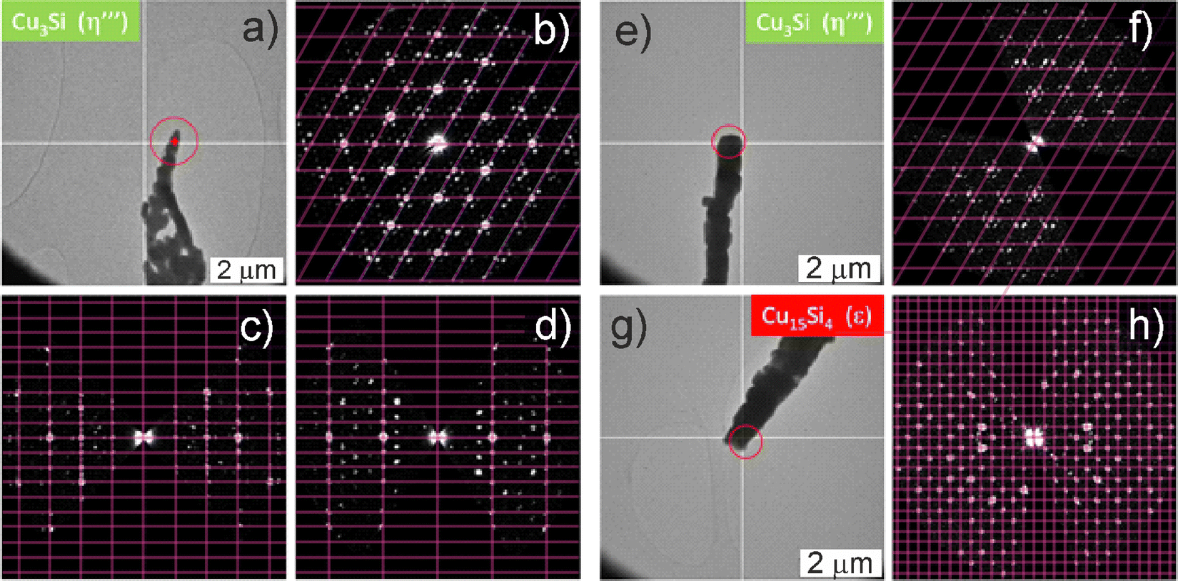 | ||
| Fig. 4 TEM/ED observations. Bluish sample on the top (a)–(d), gray-black sample at the bottom (e)–(h). (a) Image of a crystal, (b) hk0-section through 3D ED data of Cu3Si, (c) h0l-section through 3D ED data of Cu3Si, (d) −2hhl-section through 3D ED data of Cu3Si, (e) image of a crystal and (f) corresponding hk0-section through 3D ED data of Cu3Si, (g) image of a crystal and (h) corresponding hk0-section through 3D ED data of Cu15Si4. The magenta grid in the 3D ED sections represent the corresponding lattice. However, in the case of Cu3Si, which has a modulated structure, this lattice corresponds only to the main reflections whereas all the satellite reflections are not located on this grid. | ||
BET analysis was performed to estimate specific surface areas. No apparent difference was found between the gray-black and bluish deposits. The specific surface area that correlated with the active, catalytic area ranged from 0.91 to 3.29 m2 g−1. The specific surface area of the deposit surpassed the geometric area of the substrate (typically 6–7 cm × 1.3–1.4 cm) by more than two orders of magnitude. Moreover, it is essential to consider that the value of the specific surface area is merely an average figure. Specific surface areas of nanostructures (region 1), a porous layer (region 2) and a remainder of the original copper substrate (region 3) are expected to decrease in the sequence: region 1 → 2 → 3 as those nanostructures grow into themselves and form a densified porous, sponge-like matter. Consequently, one can expect that a major part of the net electrochemical reaction occurs in an environment with a specific surface area that is larger than the measured average, resulting in a gradual decrease in the reaction rates when moving from the surface to the bulk. Nitrogen physisorption measurements also provide another important parameter, the pore radius. The gray-black sample possessed a maximum pore radius of 30 nm, which was larger than the bluish one (15 nm) by a factor of two (Fig. S12, ESI†). Such pores are classified as mesopores according to IUPAC nomenclature. Neither micropores (radius < 2 nm) nor macropores (radius > 50 nm) were detected.
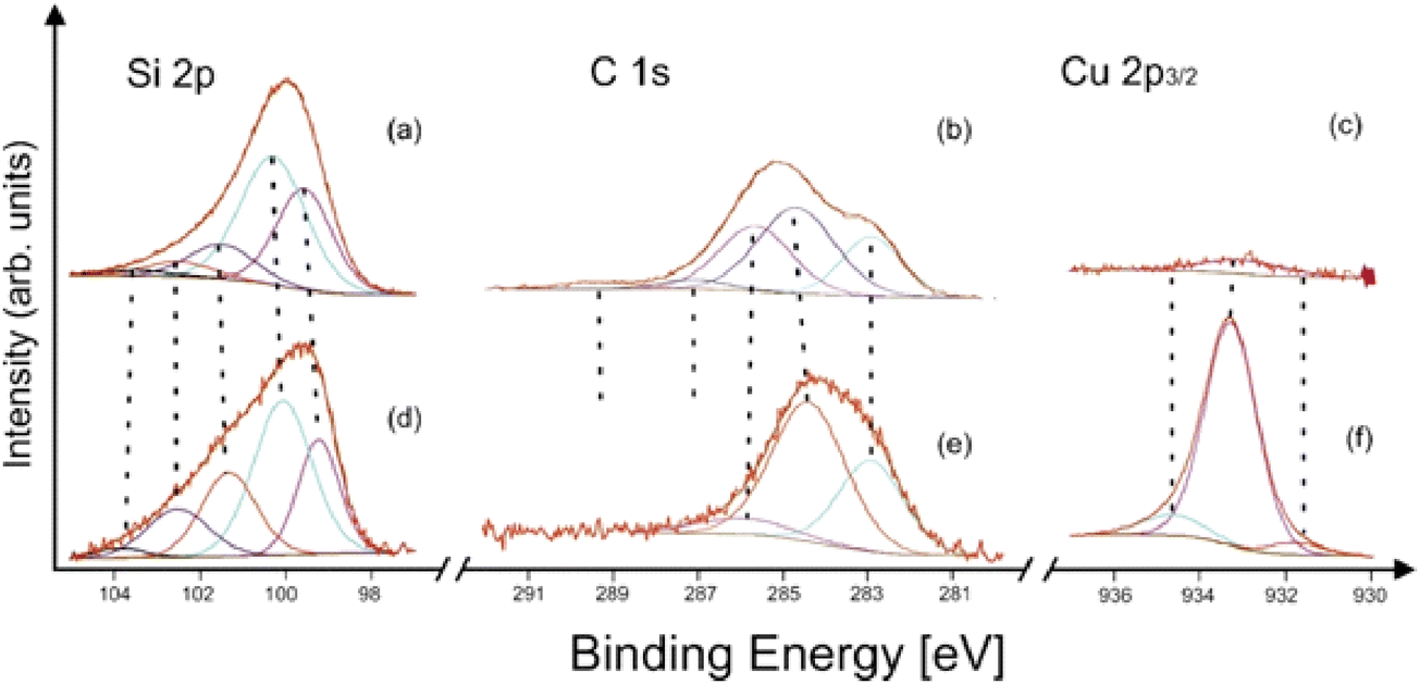
The XP spectroscopic measurements confirmed that the fundamental difference between the structures of the bluish and gray-black samples was the presence of a surface layer of silicon carbide in the former. The TEM/EDS analyses of the bluish sample (see above) showed the SiCx layer thickness in the tenths of nanometers, in its amorphous nature, and with an absence of copper. The XPS analysis of an as-prepared bluish deposit did not show any Cu 2p peak in the spectrum. After 180 s. of Ar+ ion sputtering, only a very weak Cu 2p signal was detected (Fig. 5c). Furthermore, as the SiCx covering became thinner during the sputtering, the typical silicon carbide subpeak at 283 eV in the C 1s spectrum (Fig. 5b) gradually decreased in intensity. Simultaneously, the Si 2p spectrum shows silicon carbide Si–C and elemental Si (Si0) contributions (Fig. 5a).41 On the other hand, copper in the gray-black deposit was twice as abundant unlike silicon and carbon (after 180 s Ar+ ion sputtering). The presence of elemental copper and/or copper silicide and Cu(I) was represented by strong Cu 2p peaks (Fig. 5f), without any significant shake-up satellites.42 Its main component at around 933.2 eV corresponded to Cu in silicide, in accordance with the literature42,43 and our own measurements of a Cu5Si sample used as a standard. The detailed deconvolution results, including references, are summarized in Table S2 (ESI†).
 | ||
| Fig. 5 X-ray photoelectron spectra of the (a)–(c) bluish and (d)–(f) gray-black sample after 180 s Ar+ sputtering 1 kV. | ||
After performing all the necessary electrochemical measurements, SEM, TEM/EDS and ED analyses were again performed to find any changes in the catalyst structure. The SEM images do not indicate any significant changes in the appearance of both types of catalyst (Fig. S13 and S14, ESI†). However, TEM analysis showed the overgrowths of nanoflowers on the catalyst surface (Fig. S15 and S16, ESI†). The ED addressed the nanoflowers material to the Cu and Cu2O. Both the standard and bright field TEM images indicate that copper diffuses to the surface where it partly oxidizes and forms nanoflowers from the amorphous matrix with trapped Cu2O and Cu nanocrystals. It can be seen that the nanocrystals possessed a size of about 4–5 nm and were dispersed inside the matrix (visualized in Fig. S17, ESI†).
The eCO2RR experiments were performed in a home-designed electrochemical H-cell (Fig. S2, ESI†). All electrochemical measurements were made under strict control of ambient conditions (air tightness, electrolyte tightness, temperature and proton exchange membrane (PEM) permeability). The first experiments focused on the feasibility of CO2RR in a pure carbonate electrolyte medium (purged with Ar gas) and purged with CO2 for the bluish sample.
Fig. 6 shows the linear sweep voltammogram from 0.05 V to −1.4 V vs. RHE with CO2 and argon pre-purged electrolytes (0.1 M K2CO3 at pH 10.3, and purged with CO2 at pH 6.79). It is evident that the current onset in the CO2-purged solution occurred at a slightly less negative electrode potential than in the case of the argon-purged solutions. At current densities of ca 50 μA cm−2, CO2 readily reacted at potentials more negative than −0.2 V vs. RHE. At potentials lower than −0.4 V vs. RHE, the difference between cathodic currents in the presence of CO2 and argon increased dramatically. Furthermore, it must be mentioned that for potentials lower than −0.6 V vs. RHE, the first signs of hydrogen evolution for an Ar-filled electrolyte were observed. The amount of hydrogen bubbles increased dramatically at potentials under −0.9 V vs. RHE, where HER became dominant. In the case of CO2 purged electrolyte, the first signs of hydrogen evolution were observed at −0.6 V and at −1.2 V HER became dominant, despite the measured current densities being lower than those reported for eCO2RR at ultrasmall Cu clusters in ref. 8.
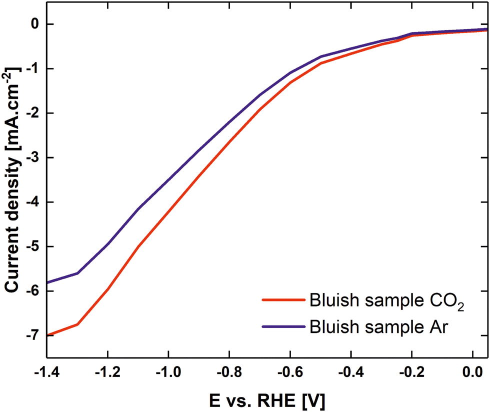 | ||
| Fig. 6 Linear sweep voltammograms of a CO2 purged 0.1 M K2CO3 electrolyte (red) to pH 6.79, Ar purged 0.1 M K2CO3 electrolyte (blue) for the bluish sample. | ||
Fig. 7 represents the dependence of products formed on the applied potentials. The trend partially follows the linear sweep voltammetry, where at potentials started at −0.45 to −0.6 V vs. RHE for the CO2 saturated electrolyte, HER accounts for nearly 20% of FE, but gradually transitions to a plateau where the ethanol formation along with acetate dominates. After a further shift of electrode potential below −0.75 V vs. RHE, eCO2RR yet again switches to the formation of hydrogen and lower C1 products. Table S3 (ESI†) summarizes the formation of various reduction products in dependence on the potential for both alkaline and neutral conditions for the bluish sample. It is worth mentioning that the selectivity of the gray-black sample towards ethanol and acetate differs significantly from the bluish one, whereby no evident trend could be detected. For the gray-black sample, oxidized C3 products – propan-2-ol, glycerol, lactic acid, acetate and ethanol dominated (Fig. S18, ESI†).
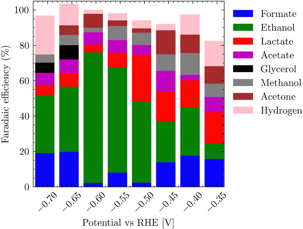 | ||
| Fig. 7 Dependence of product formation on an applied potential vs. RHE for bluish sample. | ||
The main objective for determining the applicability of the electrocatalyst was its high FE for a single product, which would represent a value-added molecule. In the case of the bluish sample, it was ethanol with a peak FE >79%, which is comparable to the highest FEs achieved in the literature for Cu-based materials.44–47 In addition, we observed comparable values for ethanol formation overpotential8,48 (−0.4 V vs. RHE). In the case of the gray sample, no dominant product was found (Fig. S18, ESI†), nor was there a trend in single product production at eCO2RR depending on the applied voltage.
Our bluish catalyst maintained high selectivity even after 700 hours, forming the reason as to why the bluish sample was chosen for a detailed study in the main electrochemical experiments. The performance of the bluish sample was double tested in a blank experiment in a 0.1 M Na2SO4 electrolyte under N2 purging, with only <0.01% of FE towards eCO2RR and more than 99.99% towards hydrogen evolution. This confirms that the detected eCO2RR products originate from CO2 reduction, and not, for example, from the decomposition of the silicon carbide shell.
The actual measurements for each potential were repeated twice for 36 h. Only when the applied potential was below −1.3 V vs. RHE, the gaseous products, namely C2H4 and CO (< 2% FE), were detected by online mass spectroscopy (Fig. S3, ESI†). Throughout the range of applied potentials, most of the products were retained in solution. The highest selectivity to ethanol (79% FE) and acetate (6% FE) was found for saturated 0.1 M K2CO3 using CO2 (20 STP mL min−1) for 30 min and an applied potential of −0.5 V vs. RHE. The corresponding NMR spectrum is shown in Fig. S19 (ESI†). The effect of pH on the selectivity of the reaction was also investigated. At pH 10.3 (0.1 M K2CO3) and an applied potential of −0.65 V vs. RHE, the highest FE was obtained for acetate (72%) and for ethanol (8%). In other words, tuning of the selectivity of eCO2RR between acetate and ethanol is possible by simply changing the pH value. The total testing time for all samples exceeded 720 hours.
Conclusions
We have synthesized a Cu-based 3D macroscopic-sized nanostructured electrocatalyst. Due to the macroscopic thickness of the active layer, which reached submillimeter dimensions, the active area of the electrocatalyst was significantly increased. For the first time, the electrochemical activity for eCO2RR was observed for copper silicide, with a unique 3D structure. Low overpotential values for ethanol or acetate generation were achieved. Moreover, it has been shown that a simple modification from neutral pH to basic pH can affect the selectivity of the whole electrochemical process from ethanol to acetate while maintaining high selectivity (>72%). The observed current densities are comparable to those of other copper compound-based materials, but do not reach the current densities of metals. The 3D structure guaranteed dominant C2+ eCO2RR products and extended its lifetime tremendously. The materials achieved similar activities and selectivities of eCO2RR to ethanol and acetate even after 720 hours of testing.Since the catalyst synthesis is based on conventional and standardized CVD, the preparation of catalysts with large surface areas is feasible. Despite the relatively low current values, high currents can be achieved at the electrode by simply increasing its size. CVD as an industry standard method facilitates the scalability of the production of the electrocatalyst and its potential deployment in eCO2RR technologies.
Author contributions
Conceptualization: V. D., data curation: J. K., J. K., K. S., formal anylysis: P. D. R. F., M. K., funding acquisition: P. D., R. B., M. K., investigation: J. K., J. K., P. S., K. S., metodology: R. F. P. S., project administration: V. J., M. K., supervision: R. B., validation: V. J., P. S., writing – original draft: V. D., writing – review & editing: P. D., M. K., R. B.Conflicts of interest
There are no conflicts to declare.Acknowledgements
The work was supported by the grant project Strategy AV21 – Hydrogen technologies funded by the Czech Academy of Sciences. CzechNanoLab project LM2023051 funded by MEYS CR is acknowledged for the greatly appreciated financial support of the measurements/sample fabrication at LNSM Research Infrastructure. R. B. acknowledges the Deutsche Forschungsgemeinschaft (DFG) – BE 5102/5-1.References
- https://www.nationalgrid.com/stories/energy-explained/what-is-ccs-how-does-it-work, accessed Jan 26, 2024.
- T. Haas, R. Krause, R. Weber, M. Demler and G. Schmid, Nat. Catal., 2017, 1, 32–39, DOI:10.1038/s41929-017-0005-1.
- H. Yoshio, K. Katsuhei and S. Shin, Chem. Lett., 1985, 1695–1698, DOI:10.1246/cl.1985.1695.
- C. Xiao and J. Zhang, ACS Nano, 2021, 15, 7975–8000, DOI:10.1126/sciadv.aay3111.
- L. Fan, C. Xia, F. Yang, J. Wang, H. Wang and Y. Lu, Sci. Adv., 2020, 6, eaay3111, DOI:10.1021/acsnano.0c10697.
- A. Bagger, W. Ju, A. S. Varela, P. Strasser and J. Rossmeisl, ChemPhysChem, 2017, 18, 3266–3273, DOI:10.1002/cphc.201700736.
- P. P. Yang, X. L. Zhang, F. Y. Gao, Y. R. Zheng, Z. Z. Niu, X. Yu, R. Liu, Z. Z. Wu, S. Qin, L. P. Chi, Y. Duan, T. Ma, X. S. Zheng, J. F. Zhu, H. J. Wang, M. R. Gao and S. H. Yu, J. Am. Chem. Soc., 2020, 142, 6400–6408, DOI:10.1021/jacs.0c01699.
- H. Xu, D. Rebollar, H. He, L. Chong, Y. Liu, C. Liu, Ch. J. Sun, T. Li, J. V. Muntean, R. E. Winans, D. J. Liu and T. Xu, Nat. Energy, 2020, 5, 623–632, DOI:10.1038/s41560-020-0666-x.
- D. Ren, J. Fong and B. S. Yeo, Nat. Commun., 2018, 9, 925, DOI:10.1038/s41467-018-03286-w.
- C. Reller, R. Krause, E. Volkova, B. Schmid, S. Neubauer, A. Rucki, M. Schuster and G. Schmid, Adv. Energy Mater., 2017, 7, 1602114, DOI:10.1002/aenm.201602114.
- A. M. Soto, J. R. Lake and K. K. Varanasi, Langmuir, 2020, 38, 1020–1033, DOI:10.1021/acs.langmuir.1c02540.
- K. Okamoto, Cu-Si (Copper-Silicon), J. Phase Equilib. Diff., 2012, 33, 415–416, DOI:10.1007/s11669-012-0076-2.
- C. A. Correa, M. Poupon, J. Kopeček, R. Král, P. Zemanová, J. Lecourt, N. Barrier, P. Brázda, M. Klementová and L. Palatinus, Intermetallics, 2017, 91, 129–139 CrossRef CAS.
- C. A. Corrêa, O. Perez, J. Kopeček, P. Brázda, M. Klementová and L. Palatinus, Acta Crystallogr., 2017, B73, 767–774, DOI:10.1107/S205252061700616344.
- R. Wongpiya, J. Ouyang, T. R. Kim, M. Deal, R. Sinclair, Y. Nishi and B. Clemens, Appl. Phys. Lett., 2013, 103, 022104, DOI:10.1063/1.4813396.
- M. A. Borek, S. Oktyabrsky, M. O. Aboelfotoh and J. Narayan, Appl. Phys. Lett., 1996, 69, 3560–3562, DOI:10.1063/1.117245.
- I. Kim, D. Byun, S. Lee and J. K. Lee, Electrochem. Acta, 2006, 52, 1532–1537, DOI:10.1016/j.electacta.2006.02.055.
- Y. Nuli, B. Wang, J. Yang, X. Yuan and Z. Ma, J. Power Sources, 2006, 153, 371–374, DOI:10.1016/j.jpowsour.2005.05.023.
- A. Slabon, S. Budnyk, E. Cuervo-Reyes, M. Woerle, C. Mensing and R. Nesper, Angew. Chem., Int. Ed., 2012, 51, 11594–11596, DOI:10.1002/anie.201203504.
- X. H. Liu, L. Q. Zhang, L. Zhong, Y. Liu, H. Zheng, J. W. Wang, J. H. Cho, S. A. Dayeh, S. T. Picraux, J. P. Sullivan, S. X. Mao, Z. Z. Ye and J. Y. Huang, Nano Lett., 2011, 11, 2251–2258, DOI:10.1021/nl200412p.
- G. A. Collins, S. Kilian, H. Geaney and K. M. Ryan, Small, 2021, 17, 2102333, DOI:10.1002/smll.202102333.
- M. R. Zamfir, H. T. Nguyen, E. Moyen, Y. H. Lee and D. Pribat, J. Mater. Chem. A, 2013, 1, 9566–9586, 10.1039/c3ta11714f.
- A. Rosenman, E. Markevich, G. Salitra, D. Aurbach, A. Garsuch and F. F. Chesneau, Adv. Energy Mater., 2015, 19, 1500212, DOI:10.1002/aenm.201500212.
- I. S. Aminu, H. Geaney, S. Imtiaz, T. E. Adegoke, N. Kapuria, G. A. Collins and K. M. Ryan, Adv. Funct. Mater., 2020, 30, 2003278, DOI:10.1002/adfm.202003278.
- P. K. Ng, B. Fisher, K. B. Low, A. Joshi-Imre, M. Bode and C. M. Lilley, J. Appl. Phys., 2012, 111, 104301, DOI:10.1063/1.4712536.
- A. R. Laracuente, L. A. Baker and L. J. Whitman, Surf. Sci., 2014, 624, 52–57, DOI:10.1016/j.susc.2013.12.006.
- S. Li, H. Cai, C. L. Gan, J. Guo, Z. Dong and J. Ma, Cryst. Growth Des., 2010, 10, 2983–2989, DOI:10.1021/cg1000232.
- Z. Zhang, L. M. Wong, H. G. Ong, X. J. Wang, J. L. Wang, S. J. Wang, H. Chen and T. Wu, Nano Lett., 2008, 8, 3205–3210, DOI:10.1021/nl8015208.
- L. Y. Ai, H. Y. Zhao, J. Wang and Y. Liu, Solid State Commun., 2017, 253, 1–5, DOI:10.1016/j.ssc.2017.01.023.
- K. Janmanchi, A. Coppernoll and D. Katsoulis, Ind. Eng. Chem. Res., 2020, 59, 3321–3333, DOI:10.1021/acs.iecr.9b06700.
- https://en.wikipedia.org/wiki/Copper_silicide, accessed Jan 26, 2024.
- M. Klementová, L. Palatinus, F. Novotný, R. Fajgar, J. Šubrt and V. Dřínek, J. Nanosci. Nanotechnol., 2013, 13, 1–9, DOI:10.1166/jnn.2013.7200.
- L. Palatinus, M. Klementová, V. Dřínek, M. Jarošová and V. Petříček, Inorg. Chem., 2011, 50, 3743–3751, DOI:10.1021/ic200102z.
- M. Klementová, L. Krabáč, P. Brázda, L. Palatinus and V. Dřínek, J. Cryst. Growth, 2017, 465, 6–11, DOI:10.1016/j.jcrysgro.2017.02.019.
- V. Dřínek, T. Křenek, M. Klementová, R. Fajgar, M. Pola, J. Savková, R. Medlín and F. Novotný, Nano, 2015, 10, 1550061, DOI:10.1142/S1793292015500617.
- T. Křenek, R. Fajgar, R. Medlín, M. Klementová, F. Novotný and V. Dřínek, J. Nanosci. Nanotechnol., 2011, 11, 1–5, DOI:10.1166/jnn.2011.5080.
- N. Mattern, R. Seyrich, L. Wilde, C. Baehtz, M. Knapp and J. Acker, J. Alloys Compd., 2007, 429, 211–215, DOI:10.1016/j.jallcom.2006.04.046.
- B. Hallstedt, J. Gröbner, M. Hampl and R. Schmid-Fetzer, Calphad, 2016, 53, 25–38, DOI:10.1016/j.calphad.2016.03.002.
- E. Y. Buchin, V. V. Naumov and S. V. Vasilyev, Semiconductors, 2019, 53, 395–399, DOI:10.1134/S1063782619030059.
- V. C. Holmberg, K. A. Collier and B. A. Korgel, Nano Lett., 2011, 11, 3803–3808, DOI:10.1021/nl201879u.
- X-ray Photoelectron Spectroscopy (XPS) Reference Pages https://www.xpsfitting.com/search/label/Silicon, accessed Jan 26, 2024.
- X-ray Photoelectron Spectroscopy (XPS) Reference Pages https://www.xpsfitting.com/search/label/Copper, accessed Jan 26, 2024.
- Y. Samson, B. Tardy, J. C. Bertolini and G. Laroze, Surf. Sci., 1995, 339, 159–170 CrossRef CAS.
- Y. S. Zhou, F. Che, M. Liu, Ch Zou, Z. Liang, P. D. Luna, H. Yuan, J. Li, Z. Wang, H. Xie, H. Li, P. Chen, E. Bladt, R. Q. Bermudez, T. K. Sham, S. Bals, J. Hofkens, D. Sinton, G. Chen and E. H. Sargent, Nat. Chem., 2018, 10, 974–980, DOI:10.1038/s41557-018-0092-x.
- D. Kim, C. S. Kley, Y. F. Li and P. D. Yang, Proc. Natl. Acad. Sci. U. S. A., 2017, 114, 10560–10565, DOI:10.1073/pnas.1711493114.
- Y. Song, R. Peng, D. K. Hensley, P. V. Bonnensen, L. Liang, Z. Wu, H. M. Meyer III, M. Chi, C. Ma, B. G. Sumpter and A. J. Rondinone, ChemistrySelect, 2016, 1, 6055–6061, DOI:10.1002/slct.201601169.
- M. S. Xie, B. Y. Xia, Y. Li, Y. Yan, Y. Yang, Q. Sun, S. H. Chan, A. Fisher and X. Wang, Energy Environ. Sci., 2016, 9, 1687–1695, 10.1039/C5EE03694A.
- K. P. Kuhl, E. R. Cave, D. N. Abram and T. F. Jaramillo, Energy Environ. Sci., 2012, 5, 7050–7059, 10.1039/C2EE21234J.
Footnote |
| † Electronic supplementary information (ESI) available. See DOI: https://doi.org/10.1039/d3ma00633f |
| This journal is © The Royal Society of Chemistry 2024 |