 Open Access Article
Creative Commons Attribution 3.0 Unported Licence
Structure, surface/interface chemistry and optical properties of W-incorporated β-Ga2O3 films made by pulsed laser deposition
Francelia
Sanchez
ab,
Debabrata
Das
ac,
Nathan
Episcopo
ac,
Felicia S.
Manciu
d,
Susheng
Tan
 e,
Vaithiyalingam
Shutthanandan
 f and
C. V.
Ramana
 *acg
*acg
aCenter for Advanced Materials Research (CMR), University of Texas at El Paso, 500 W University Ave, El Paso, Texas 79968, USA. E-mail: rvchintalapalle@utep.edu
bDepartment of Metallurgical, Materials, and Biomaterials Engineering, University of Texas at El Paso, 500 W University Ave, El Paso, Texas 79968, USA
cDepartment of Aerospace and Mechanical Engineering, University of Texas at El Paso, 500 W University Ave, El Paso, Texas 79968, USA
dDepartment of Physics, University of Texas at El Paso, 500 W University Ave, El Paso, Texas 79968, USA
eDepartment of Electrical and Computer Engineering and Petersen Institute of Nano Science and Engineering, University of Pittsburgh, Pittsburgh, PA 15261, USA
fEnvironmental Molecular Sciences Laboratory, Pacific Northwest National Laboratory, 902 Battelle Blvd, Richland, Washington 99354, USA
gPhysical and Computational Sciences Directorate (PCSD), Pacific Northwest National Laboratory (PNNL), Richland, WA 99352, USA
First published on 6th September 2024
Abstract
Gallium oxide (Ga2O3), which is one among the ultra-wide band gap materials, is promising for the next generation of electronic and optoelectronic devices due to its fascinating material properties for utilization in extreme environments. In this work, Ga2O3 films containing refractory tungsten (W) (GWO or Ga–W–O) were fabricated via pulsed laser deposition (PLD) by varying the oxygen partial pressure (pO2), which is the most important thermodynamic parameter that governs the growth, structure and properties of the resulting multi-component oxide films. The effect of variable pO2 on the structure, surface chemistry, chemical bonding, optical properties and photodetector device performance of the resulting Ga–W–O films was studied using X-ray photoelectron spectroscopy, Raman spectroscopy, atomic force microscopy, UV-vis spectroscopy, and photoluminescence spectroscopy measurements. The films containing Ga2O3 combined with W exhibited no secondary phase development. The impact of W on the chemical and optical characteristics of Ga2O3 films was found to be substantial. W5+ formation is prevalent when the adatom mobility is high at lower working pressure, whereas lower migration energy favors W6+ at higher working pressure. In contrast, the valance band maxima (VBM) of the films have a minor shift to higher energies with increasing pO2, confirming the dominance of O 2p states on VBM in PLD GWO films. Additionally, there is not much change in the optical band gap, but it shows a slight blue shift of the luminescence peak, directing a selective W incorporation into the Ga2O3 matrix. The processing conditions were optimized to demonstrate the excellent performance UV-photodetectors based on PLD GWO films. The structure–property correlation established will be useful in the production of W-alloyed β-Ga2O3 films with superior structural and optical properties for integration into optoelectronic and photonic device applications.
1. Introduction
Among ultra-wide band gap (UWBG) oxide materials, gallium oxide (Ga2O3) is investigated as a promising candidate for the next generation of electronic and optoelectronic devices due to its desirable intrinsic material properties. Ga2O3 exhibits polymorphism and consists of six crystal structures: the rhombohedral α, monoclinic β, cubic γ, cubic δ, hexagonal ε, and orthorhombic κ phases.1,2 Nevertheless, β-Ga2O3 received tremendous interest due to its chemical and thermal stability throughout all temperature ranges, from room temperature to its high melting point of ∼1800 °C.3 Further, high-quality β-Ga2O3 crystals that allow the growth of homoepitaxial films are readily available as they can be fabricated from the melt using the Czochralski, floating-zone, and edge-defined fed methods.4 β-Ga2O3 is attractive due to its UWBG of ∼4.9 eV and high theoretical breakdown field of 8 MV cm−1. Some of the explored applications of β-Ga2O3 include high-power electronic devices, solar-blind photodetectors, light-emitting diodes (LEDs), chemical sensors, field-effect transistors (FETs), photocatalysis, etc.3,5–9Historically, doping and alloying of semiconductors have been employed to tailor the structural, electrical, and optical properties.10,11 N-type Si-doping is the preferred method to control the electrical conductivity of β-Ga2O3 as the shallow donor successfully increases the concentration of free carriers by three orders of magnitude.4,12 Further, because of their multiple states of charge, doping with transition metals (TMs) may promote more than one energy level.13 Fe-dopant is a useful deep-level acceptor as it compensates background n-type carriers. Fe-doped β-Ga2O3 is commonly used as a semi-insulating crystalline substrate to grow homoepitaxial contact layers in β-Ga2O3 devices.14,15 Semi-insulating substrates are desired to prevent conduction losses that causes degradation in device performance.9 Moreover, doping with transition and rare earth elements (REs) into Ga2O3 has demonstrated interesting photoluminescence and electroluminescence properties.7,8,11,15,16 Intentional doping with TMs and REs can facilitate light emissions in a broad spectral range, from ultraviolet (UV) to near-infrared (NIR). Solar-blind UV photodetectors were fabricated using Sn, Ta, and W dopants.3,5,17 Cr-doped Ga2O3 exhibits strong NIR luminescence, which is desired to develop real-time optical imaging.16 Further, monolithic, phosphor-free, multi-color LEDs was achieved from the pulsed laser deposition (PLD) of Ga2O3:(Tm + Eu + Er) multilayers on GaN and GaAs substrates as Eu, Er, and Tm doping intensify red, green, and blue electroluminescence emissions, respectively.7,8 Undoubtedly, the tunable optical and electrical properties of Ga2O3 have potential for the design and development of next generation of electronic and optoelectronic devices.
In the present work, W-incorporated β-Ga2O3 thin films were fabricated by PLD. High-solubility of W ions into the β-Ga2O3 matrix and tuning of the electrical have been demonstrated elsewhere.3,18–20 Our interest in the PLD W–Ga2O3 films is primarily towards the design and development of robust and advanced deep UV photodetectors for functionality in extreme conditions. Considering W-incorporation into Ga2O3 is due to the following fundamental scientific reasons. Tungsten is a refractory metal and has been considered as the potential contact layer for high-frequency electronic devices based on Ga2O3.21,22 Additionally, tungsten oxide (WxOy) is also an attractive multifunctional material due to its intrinsic properties, including structural flexibility, the high melting temperature of approximately 1470 °C, and chromogenic behavior.23–26 It has a wide range of applications in the energy sector, involving chromogenic devices to fabricate smart windows and photocatalysts to harvest solar energy.24 WxOy has been applied to gas sensors, water splitting, memory devices, and high-temperature diodes as a thin film.23 Therefore, even if the processing conditions result in composite phase formation which occurs with individual component oxides in the matrix, excellent means to control the properties and performance is expected by taking the advantage of both Ga2O3 and WO3. Moreover, the properties and performance of thin film-based devices strongly depend on the crystal quality of the films. Therefore, processing under optimum conditions of W-incorporated Ga2O3 expected to provide materials useful for electronic and optoelectronic device applications. However, understanding the interplay between processing conditions, surface/interface microstructure, and optical properties is quite important in order to optimize the materials for enhanced performance in the device applications. In PLD, processing parameters such as temperature, atmospheric pressure, gas species, target material, and laser conditions influences the growth and structure of the resulting films and can be controlled to improve the properties and quality of the films.3,11,27 Therefore, in this work, the effect of varying oxygen partial pressure (pO2) on the optical properties, electronic structure, chemical composition, and morphology of the W-incorporated β-Ga2O3 films was investigated using multiple surface/interface characterization techniques in addition to probing material properties under variable growth conditions. We demonstrate that precise control over the deposition parameters allows tuning of the structure and optical properties of the Ga–W–O thin films for application in advanced, deep-UV photodetectors.
2. Experimental details
2.1. Materials and PLD target synthesis
Tungsten-incorporated β-Ga2O3 (hereafter, referred to GWO or Ga–W–O) PLD target was synthesized using the conventional solid-state reaction method. High-purity WO3 (99.999%, Sigma Aldrich) and β-Ga2O3 (99.999%, Sigma Aldrich) powder precursors were weighed in stoichiometric proportions according to the chemical formula Ga2−xWxO3 where x = 0.1. The powders were ground in an agate mortar under a volatile liquid environment (acetone) to decrease the particle size and ensure homogeneity. The homogeneous mixture was calcined in a SentroTech muffle furnace at 1100 °C for 12 h with a heating and cooling ramp rate of 5 °C min−1.3,18,28–31 The calcinated powder was mixed with polyvinyl alcohol (PVA) binder to create the target. The mixture was pressed using a uniaxial hydraulic press with an applied load of 1.5 tons for 3 min to shape the circular pellet with dimensions of 25.4 mm diameter and 5 mm thickness. The pellet was heated at 100 °C for 60 min to burn the binder material. After binder burnout, the pellet was sintered at 1350 °C for 12 h using a heating and cooling ramp rate of 5 °C min−1.3,18,28–31 The PLD target was examined thoroughly for structure, composition, and mechanical integrity to serve as a target for laser ablation before introducing it into PLD chamber for thin film deposition.2.2. Pulsed laser deposition of GWO thin films
The GWO thin films were deposited onto Si(100) substrates by PLD. A KrF excimer laser with a wavelength of 248 nm and a pulse energy of 220 mJ was employed for the deposition process. The distance between the target and substrate was fixed at 45 mm. The substrate temperature and pulsed laser frequency were set at a constant value of 700 °C and 3 Hz, respectively. Note that, the substrate temperature (Ts) and oxygen partial pressure (pO2) are the two most important thermodynamic parameters that govern the film growth behavior and structure of the materials. While our previous work demonstrated that Ts = 700 °C is optimum to provide the sufficient thermal energy to promote the growth of crystalline films, in this work, pO2 is varied in the range of 5–200 mTorr during deposition process.3 The resulting films were subjected to extensive characterization in order to understand the effect of oxygen pressure on the surface/interface chemistry and optical properties of PLD grown GWO films.2.3. Characterization
3. Results and discussion
3.1. Surface chemistry, electronic structure and chemical bonding
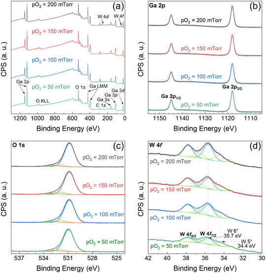
The elemental composition, chemical state, and electronic configuration were investigated using XPS. In Fig. 1(a), wide scan survey spectra confirm the presence of gallium (Ga), tungsten (W), and oxygen (O) XPS peaks. In addition, C 1s peak was identified due to carbon adsorption from exposure to air during the transfer of the samples to the XPS instrument. High-resolution XPS spectra of Ga 2p, O 1s, W 4f, and C 1s (not shown) were obtained to analyze each photoelectron region in greater detail. The binding energy (BE) scale of the scans was calibrated using a charge reference of the adventitious C–C/C–H peak to 284.8 eV.33 The asymmetric O 1s peak, shown in Fig. 1(c), was deconvoluted into three components after subtraction of a Shirley background. The main peak with high intensity is centered at 530.85 ± 0.05 eV, corresponding to the metal oxide lattice bonds between Ga and O or W and O. The shoulder peaks at higher binding energies demonstrate partial surface contamination caused by sample handling. The peaks positioned at 532 and 533 eV are assigned to the covalent bonds between carbon and O in the organic hydroxyl (C–O) and carbonyl (C![[double bond, length as m-dash]](https://www.rsc.org/images/entities/char_e001.gif) O) groups, respectively.18,28,34
O) groups, respectively.18,28,34
The high-resolution Ga 2p core level spectra are illustrated in Fig. 1(b). The data shown are for GWO samples deposited at different pO2. For further analyses and to probe changes in chemical stoichiometry as a function of pO2 and W-incorporation, the Ga 2p core level was preferred over Ga 3d because of its high intensity and isolated position, avoiding interference or overlapping with other electron peaks. The peaks identified correspond to the doublet Ga 2p3/2 and Ga 2p1/2. The former peak positioned at a BE ∼ 1118.1 ± 0.1 eV is attributed to the Ga3+ ions of stoichiometric Ga2O3.18,28–30 The doublet peaks have a spin–orbit splitting (ΔE = BE Ga 2p3/2 − BE Ga 2p1/2) of 26.9 eV. As shown in Fig. 1(b), there is no appreciable change in the shape and position of the Ga peaks. Therefore, the chemical valence state of Ga ions is very stable throughout the PLD deposited W-incorporated β-Ga2O3 samples despite the W incorporation and the varying pO2 during deposition.
Detailed core level spectra of the W 4f are depicted in Fig. 1(d). The analysis of the W 4f spectra is difficult because of its changing background, the possible presence of multiple chemical states, and the proximity to the W 5p3/2 region.35,36 The iterative Shirley method was used to correct the complex background with step changes.35 The doublet, namely W 4f7/2 and W f5/2, is visibly identified on the spectra. Distinctly, peaks are asymmetric due to the co-existence of more than one valence state of W within the surface of the PLD GWO films. The binding energies of W0, W4+, W5+, and W6+ in the W 4f7/2 region are reported to be at 31.4, 32.9, 34.6, and 35.9 ± 0.2 eV, respectively.36 The W 4f spectra were deconvoluted into two components using a mixed Gaussian–Lorentzian (GL30) line shape. The higher binding energy peak is centered at 35.7 eV, corresponding to the highest valence state of W, W6+. The shoulder peak on the right is positioned at a lower binding energy of 34.4 eV and is assigned to reduced W5+ ions. In fact, the WxOy chemistry is very complex because of its structural flexibility and cation intermediate states.24,36 The W–O system contains numerous oxides with variable chemical valence states, namely, WO3, WO2.9, W3O8, W5O14, W18O49, and W24O68, among others.24,25 The reduced oxides commonly occur as the lattice can sustain high O vacancies and partially reduced W5+ species. The electronic density near the W valence states increases with O vacancies since the electronegativity of O is greater than W.37,38 Therefore, the electron binding energy of W5+ is in lower energy levels because of the high concentration of electrons surrounding it. Furthermore, the W 4f peaks show a gradual increase in peak intensity as a function of pO2. Evidently, the W content increases with increasing pO2. In addition, the peaks in Ga 2p and W 4f have minimal narrowing with the increasing pressure. Decay in full width at half maximum (FWHM) may be caused by improvement in the crystallinity of the films.39
The chemical and electronic structures of the films are highly dependent on their growing conditions.40 In depositing complex multicomponent target material such as β-Ga2−xWxO3, the discrete plasma plume species travel at different velocities because of their dissimilar ionic mass and size.41 Background gas pressure can control the number of collisions between gas and plasma plume species. Consequently, background pressure tailors the kinetic energy of the species arriving on the substrate. The mean free path (MFP) is the ratio between the distance traveled and the number of collisions between species, which is approximated using the equation:
 | (1) |
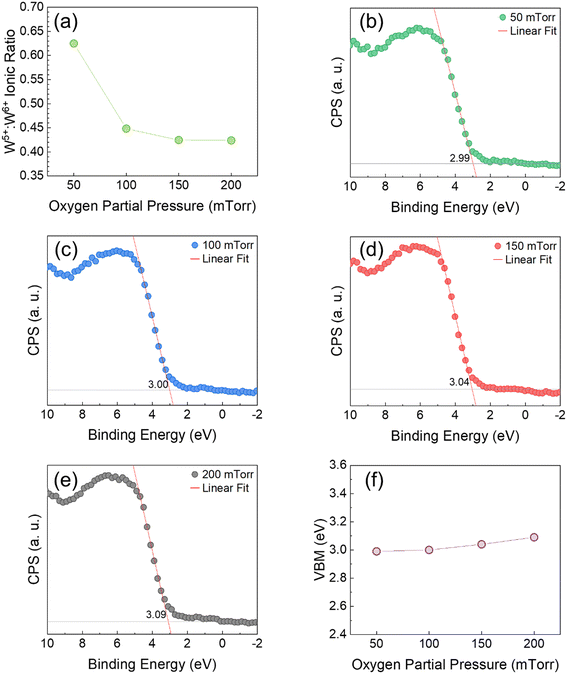
Furthermore, the changes in stoichiometry and electronic structure, such as W content and valence states, are attributed to the varying pressure. Though the ionic size between Ga and W is similar, W content at the surface varies with gas pressure. Fig. 2(a) depicts the ratio of W5+![[thin space (1/6-em)]](https://www.rsc.org/images/entities/char_2009.gif) :
:![[thin space (1/6-em)]](https://www.rsc.org/images/entities/char_2009.gif) W6+ ions as a function of pO2. W is deficient at the lower pO2, whereas its incorporation improves as the pressure increases. First, there is a greater amount of Ga ions in the plasma plume because of the Ga-rich target composition. For this reason, the Ga content is high and very stable in all the samples, as demonstrated by XPS analysis. Moreover, the lower content of W ions is slightly smaller than that of Ga ions.43,44 Thus, at a given pressure, W species have greater migration energy than Ga. In vacuum-like pressure, the W ions travel with high kinetic energy and are more likely to outdiffuse from the surface of the substrate.3 With the increasing pressure, the migration energy of the W species decreases as a result of greater interaction between O and the plasma plume species. These collisions promote nuclei and cluster formation. Consequently, W incorporation is improved in the films. This pressure regime is known as diffusion-like growth. However, the presence of W5+ is accompanied by O defects on the surface. Clearly, the amount of W5+ species decreases with the increasing pressure. The formation of W5+ indicates non-stoichiometric growth of reduced W6+ due to O deficiency.37,38,45–49 Note that the ionic ratio is drastically higher when the film is deposited at a pO2 of 50 mTorr in comparison with higher pO2. O-vacancies can easily form in vacuum-like low pressures due to insufficient interaction between background gas and plasma plume species. Nevertheless, the formation energy of O vacancies increases with higher pO2.50,51 The incorporation of O species in the film is improved by increasing collisions between gas and plasma plume species. As a result, the structural quality of the film increases. Overall, W5+ formation is prevalent when the adatom mobility is high, and it is observed with higher temperature, lower working pressure, or lower laser power density. In contrast, lower migration energy favors W6+.38,46–49,52–55 Additionally, the crystal structure of the samples improves as the concentration of O defects decreases with the higher background pressures. Conclusively, the formation of W5+ reduced ions, increasing W content, and improving crystalline structure are a result of the dissimilar mean free path of the species with varying pO2. Thus, the XPS studies indicate that a pO2 of 100 mTorr or higher will be needed in order to realize GWO films without any compositional defects, particularly those related to reduced states of W-ions. Such defects may introduce additional localized states in the electronic structure and can shift the band gap dramatically. This scenario will result in the performance degradation of UV-photodetector based on GWO films.
W6+ ions as a function of pO2. W is deficient at the lower pO2, whereas its incorporation improves as the pressure increases. First, there is a greater amount of Ga ions in the plasma plume because of the Ga-rich target composition. For this reason, the Ga content is high and very stable in all the samples, as demonstrated by XPS analysis. Moreover, the lower content of W ions is slightly smaller than that of Ga ions.43,44 Thus, at a given pressure, W species have greater migration energy than Ga. In vacuum-like pressure, the W ions travel with high kinetic energy and are more likely to outdiffuse from the surface of the substrate.3 With the increasing pressure, the migration energy of the W species decreases as a result of greater interaction between O and the plasma plume species. These collisions promote nuclei and cluster formation. Consequently, W incorporation is improved in the films. This pressure regime is known as diffusion-like growth. However, the presence of W5+ is accompanied by O defects on the surface. Clearly, the amount of W5+ species decreases with the increasing pressure. The formation of W5+ indicates non-stoichiometric growth of reduced W6+ due to O deficiency.37,38,45–49 Note that the ionic ratio is drastically higher when the film is deposited at a pO2 of 50 mTorr in comparison with higher pO2. O-vacancies can easily form in vacuum-like low pressures due to insufficient interaction between background gas and plasma plume species. Nevertheless, the formation energy of O vacancies increases with higher pO2.50,51 The incorporation of O species in the film is improved by increasing collisions between gas and plasma plume species. As a result, the structural quality of the film increases. Overall, W5+ formation is prevalent when the adatom mobility is high, and it is observed with higher temperature, lower working pressure, or lower laser power density. In contrast, lower migration energy favors W6+.38,46–49,52–55 Additionally, the crystal structure of the samples improves as the concentration of O defects decreases with the higher background pressures. Conclusively, the formation of W5+ reduced ions, increasing W content, and improving crystalline structure are a result of the dissimilar mean free path of the species with varying pO2. Thus, the XPS studies indicate that a pO2 of 100 mTorr or higher will be needed in order to realize GWO films without any compositional defects, particularly those related to reduced states of W-ions. Such defects may introduce additional localized states in the electronic structure and can shift the band gap dramatically. This scenario will result in the performance degradation of UV-photodetector based on GWO films.
Having understood the chemistry of GWO films using core-level XPS, we now direct our attention to the density of electronic states. The high-resolution valence band XPS spectra demonstrate the density of electronic states in the lowest BE region. In addition, it can provide the valence band maxima and the Fermi-level position relative to VBM.28 In Fig. 2(b–e), the valence band maxima (VBM) of the samples were determined from the linear extrapolation of the leading edge to the background line at zero counts in the valence band spectra. The Fermi-level position with respect to the surface VBM is defined by the BE corresponding to 0 eV. The linear extrapolation of the leading edge in the valence band spectra of Ga2O3 is simple and has been used in multiple XPS analyses of different materials. The VBM of films may vary due to processing conditions, microstructure, elemental composition, defects, etc.28,34,56–60 The VBM of the samples as a function of pO2 is depicted in Fig. 2(f). As seen, the VBM of the films has a minor shift to higher energies with increasing pO2. It is believed that the changes in VBM are associated with the varying W content rather than lattice defects, as there are no significant changes in the position and shape of Ga 2p peaks in Fig. 1(b). The minimum increase in VBM with the increasing W concentration is expected as O 2p states dominate the VBM.57–59
The Raman spectra of GWO grown at different pO2 pressures are shown in Fig. 3a. For comparison, the spectrum of bulk monoclinic β-Ga2O3 is also presented in Fig. 3b. The latter is shown for easier observation of potential changes of β-Ga2O3 vibrational lines with W incorporation. There is no visible difference between the spectra of GWO due to pO2 pressure growth. While in the low- and mid-frequency regions (120–550 cm−1), the strong Si peak at 521 cm−1 and the unwanted but conspicuous presence of Si–O bonds at 303 cm−1 dominate the spectra of GWO. However, the two weak shoulders at 170 cm−1 and 232 cm−1 could infer the presence of β-Ga2O3.61 The latter is blue-shifted by 33 cm−1 from the characteristic vibrational line at 199 cm−1 (Ag). Similarly, the weak feature at 435 cm−1 can be attributed to a shifted β-Ga2O3 vibration at 415 cm−1 (Ag). It can also be associated with SiO2 presence. Shifts in phonon frequencies due to size confinement effects are expected and have been reported in low-dimensional materials.62 Additionally, the vibrational modes can experience positive or negative shift when the dopant into host matrix is different in terms of atomic mass despite the solid solubility.63 The small thickness of the GWO film, in addition to contributing to the weakness of vibrational lines associated with the material of interest, cannot mask the strong presence of Si and SiO2 seen. Other peaks in the high-frequency region (500–770 cm−1) associated with O–Ga–O stretching and bending modes of GaO4 units of β-Ga2O3 are observed at 625 and 675 cm−1 in the GWO spectrum. They are attributed to the red and blue shifted lines at 629 and 657 cm−1 of β-Ga2O3, respectively. The disappearance of the 767 cm−1 vibration of β-Ga2O3 and the appearance of the weak and broad band at 820 cm−1 in the GWO spectrum is potentially correlated with the incorporation of W into the gallium oxide structure by substitution of W-ions at the Ga-ions sides and formation of vacancies.
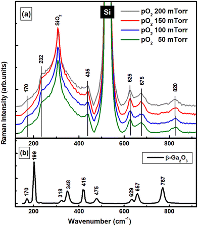 | ||
| Fig. 3 (a) Raman spectra of W-incorporated β-Ga2O3 films deposited under variable pO2. (b) Raman spectrum of bulk β-Ga2O3. | ||
3.2. Morphology and microstructure
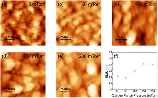
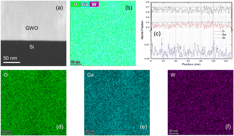
The surface morphology of PLD deposited GWO films was analyzed using the AFM measurements. The 2D topographical scans of the W-incorporated β-Ga2O3 films are shown in Fig. 4(a–e). In addition, the root-mean-square surface roughness was calculated to quantify the effect of pO2 on the surface morphology of the PLD GWO films. There is an evidence for the granular morphology of the PLD GWO films, where that the nanoscale grain structure increases in size with increasing pO2. This observation is commonly observed in many of the simple and complex metal-oxide films made by PLD, specifically for samples grown under increasing pO2.64–66 In fact, at least for the specific case of PLD oxide films, increasing pO2 induces the grain-growth under the reactive atmosphere, which in turn roughens the samples' surface leading to changes in the optical properties.65 On the other hand, comparable to XPS data revealing the chemical composition and complex chemistry of W-ions under variable pO2, the AFM results are highly susceptible to the growth kinetics of the films. In Fig. 4(a), the scanned image of the film deposited at a low pO2 of 5 mTorr reveals a non-uniform surface. As discussed earlier, due to the minimal interaction between gas and plasma plume species, poor crystallinity, low roughness, and high concentration of surface defects, such as O vacancies, are expected in films grown at vacuum-like pressures. With the increasing pressure, at 50 mTorr, the surface is somewhat uniform, and the grain structure is well defined. Furthermore, the roughness slightly decreases, which might be due to the fulfillment of O-vacancies. As the pO2 increases, the film grows in a diffusion-like regime, where the roughness increases due to the larger crystals formed from the undergoing cluster growth. Even at a higher pressure of 200 mTorr, the roughness is relatively non-affected by the higher pO2. Overall, an increased O gas pressure leads to the formation of denser and more uniform films with larger grain sizes. Additionally, surface features have a great effect on the optical properties of films.34,48 On the other hand, PLD GWO film thickness is varying from ∼50 to ∼200 nm with pO2 but we believe the effect of the AFM on surfaces is a true reflection of the effect of pO2 instead of thickness since we made extensive studies previously on pure Ga2O3 films with variable thickness. Thus, the XPS and AFM studies indicate that the stoichiometric GWO film growth with good surface morphology can be obtained for pO2 of 100 mTorr and higher.After understanding the surface chemistry and morphology of the PLD GWO films, we directed our efforts to understand their microstructure and surface/interface chemical composition profiles using high-resolution transmission electron microscopy (HRTEM) studies. Fig. 5 depicts the high-resolution cross-sectional morphology and elemental color mapping of a representative PLD GWO film (pO2 = 100 mTorr) on Si substrate. Cross-sectional HAADF-STEM image (Fig. 5a) clearly shows the presence of sharp transition from the substrate to the W-incorporated β-Ga2O3 film at the interface. There is no evidence of Ga assisted reverse etching of the substrate during the first nucleation phase at the start of the growth process. Additionally, the elemental color mapping and the atomic percentage plots (Fig. 5b and c) confirm the presence of evenly distributed O, Ga, and W atoms. Also, their relative percentages match the stoichiometry, highest for O and lowest for W.
Finally, before proceeding to evaluate the optical properties of PLD GWO films, we present a brief summary of crystal structure analyses made by X-ray diffraction (XRD) studies. The effect of pO2 on the crystal structure and phase stabilization of GWO films has been reported elsewhere in detail.3 In XRD, all the peaks observed were in excellent agreement with β-phase Ga2O3 and no diffraction peaks due to WO3 were observed. However, somewhat broader and asymmetric peaks related to β-Ga2O3 were noted. When these results combined with aforementioned Raman spectroscopic data, it appears that heavier W ions substituting for relatively lighter Ga ions may cause some lattice strain. On the other hand, the difference in the ionic radii of Ga3+ and W6+ is relatively small (the ionic radius of Ga3+ and W6+ is 0.062 and 0.060 nm, respectively) suggesting the solid solution should be possible provided the temperature and oxygen pressure are optimum. Indeed, the XRD studies indicated that the PLD GWO films were crystallized in β-phase Ga2O3.3 However, GWO films deposited at relatively lower pO2 (5–50 mTorr) are of not high quality while those deposited at higher pO2 were textured and stabilize in β-Ga2O3 films. The crystal quality improves with increasing pO2 for the PLD GWO films. Therefore, summarizing intermittently based on the structure, surface chemistry, chemical bonding, and surface morphology studies of PLD GWO films deposited at variable pO2, oxygen pressure of 100 mTorr or higher results in the stoichiometric, crystalline GWO films with β-phase and good surface quality as desired for UV-photodetector applications.
3.3. Optical properties
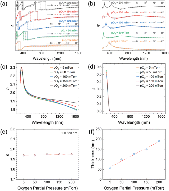
 | (2) |
 | (3) |
 | (4) |
3.4. UV-vis spectroscopy
UV-vis diffuse reflectance spectrum of the W-incorporated β-Ga2O3 films on a silicon substrate was obtained to derive the bandgap of the films. Since the band gap energy transition (Eg) is not as notorious in the diffuse reflectance spectra, the reflectance spectra were converted to the Kubelka–Munk (K–M) function, which is directly proportional to the absorption coefficient as follows: | (5) |
| (αhv)n = A(hv − Eg) | (6) |
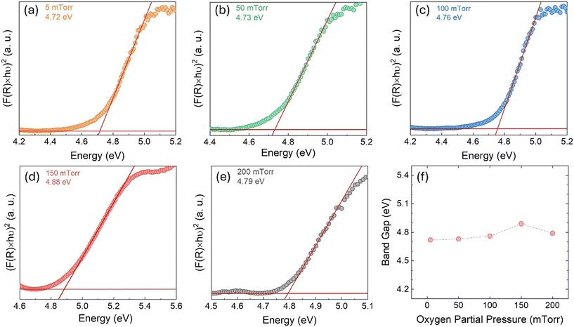 | ||
| Fig. 7 (a–e) Tauc plots originated from UV-vis reflectance spectra for bandgap calculation using linear extrapolation. (f) Bandgap energy variation as a function of pO2. | ||
3.5. Photoluminescence spectroscopy
Photoluminescence (PL) measurements were obtained to further understand the electronic structure and defect states of the W-incorporated β-Ga2O3 films with varying pO2. PL spectroscopy is very useful in characterizing semiconductor materials because it reveals the recombination dynamics of photo-generated carriers and detects optically active intrinsic and extrinsic defect states.3,74 The room temperature steady-state PL spectra of the W-incorporated β-Ga2O3 films are illustrated in Fig. 8. The PL data was collected in the wavelength range of 250 to 800 nm. The PL spectra of each sample exhibit an asymmetric peak due to the presence of multiple luminescence bands. The luminescence behavior of β-Ga2O3 is well-established in the literature. The peak position and peak intensity of the PL transitions depend on the trap-state density of the films that were manipulated by adjusting the deposition conditions, such as substrate temperature and working pressure. In the W-incorporated β-Ga2O3 films, three PL bands corresponding to blue, green, and red emissions are observed. The blue and green emissions are reported to originate from recombining the donor–acceptor pair (DAP). In the blue band, the Ga–O pair and Ga vacancies (VGa) act as the acceptor, and O vacancies (VO) correspond to the donor, and in the green emissions, the VO and Gai serve as donors.75,76 Clearly, there is a gradual red shift of the peaks with increasing deposition pressure. As observed in XPS results, the W content in the films increases with pressure. Thus, the gradual red shift of the peaks is associated with the incorporation of W.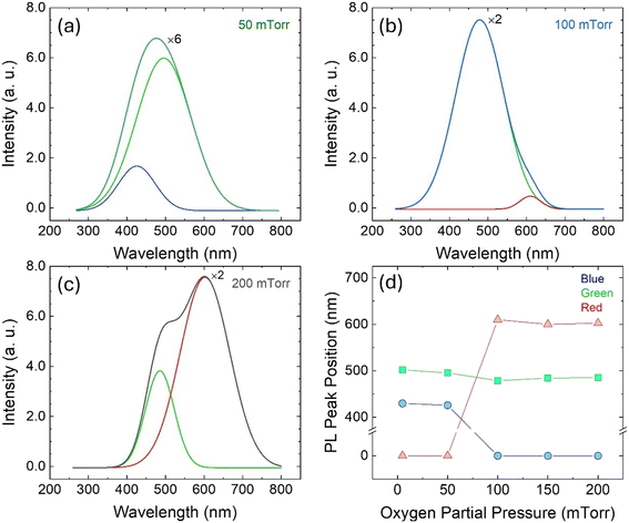 | ||
| Fig. 8 (a–c) Room temperature PL spectroscopy of the W-incorporated β-Ga2O3 films. (d) PL peak position as a function of pO2. | ||
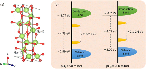
Substitutional W in β-Ga2O3 is a potential triple donor since W at Ga sites can provide a maximum of three extra electrons.77 W atoms in β-Ga2O3 may occupy tetrahedral or octahedral sites. The inequivalent Ga sites in the unit cell of β-Ga2O3 are depicted in Fig. 9(a). Octahedrally coordinated W serves as a deep donor and has a lower formation energy than W on tetrahedral sites, which acts as a shallow donor. The formation energy of W on octahedral sites is lower because of the lower Fermi-level position of the charge-state transition levels and smaller local distortion in the lattice.77 Therefore, there is a preferential formation of substitutional W on octahedral positions that serve as deep donors and introduce the red PL emission. The empirical valence and conduction band diagram calculated from the XPS, UV-vis, and PL spectra analysis of the W-incorporated β-Ga2O3 films grown under different pO2 are shown in Fig. 9(b). The slight changes in the density of states diagram are associated with the varying elemental composition and concentration of defect states. The increase in the VBM in O2-rich environment is caused by the higher W content, whereas the band gap narrowing in O2-poor conditions is due to the high concentration of O vacancies.
By establishing a correlation between chemical, optical, and luminescence properties, it can be inferred that the development of W-incorporated β-Ga2O3 thin films with tunable emission bandwidth is significantly influenced by the pO2. By employing meticulously regulated in situ variables, it becomes feasible to exhibit superior stoichiometric W-incorporated β-Ga2O3 on external substrates, enabling its subsequent use as effective visible-emitting phosphors in smart LED applications. In tandem with the development of contemporary civilization and technological progress, the global community is moving towards effectively utilizing current energy sources. To address this issue, a crucial measure is to eradicate ineffective artificial light sources and substitute them with intelligent, energy-efficient phosphor-converted light-emitting diodes (pc-LEDs). The current state of pc-LEDs mainly depends on rare earth (RE) minerals as either bulk or dopants, which poses challenges in terms of energy efficiency due to their toxicity and limited availability.7,8 The W-incorporated β-Ga2O3 thin films stated above can be a strong alternative to RE-based phosphors and can be easily integrated with current semiconductor nanofabrication methods for pc-LEDs.
3.6. Deep-UV photodetection
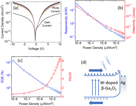
We have constructed a basic metal–semiconductor–metal (1 × 1 mm MSM) ultraviolet photodetector (PD), in which W-doped β-Ga2O3 is used as the active material and a silver top metal contact is employed. Since the fundamental material characterization using a wide variety of surface analytical techniques indicated that the samples deposited at lower pO2 were containing various defects and pO2 ∼ 100 mTorr was optimum to produce GWO films with better quality, the photodetector sandwich structures were made on PLD GWO films made at 100 mTorr. The simple manufacturing procedure and low-cost metal contact were chosen to show a cost-effective UV solar-blind photodetection method. Significantly, the Ag and W-doped β-Ga2O3 are establishing a Schottky contact, as seen in Fig. 10. The metal–semiconductor interface's carrier exchange process is mostly controlled by thermionic emission, which needs a lot of energy to get past the normal Schottky junction limit. Moreover, there exists a specific likelihood of thermionic field emission or field emission-assisted tunneling occurring throughout the depletion zone. The metal–semiconductor interface trap states are crucial to tunneling.We used 265 nm photoexcitation and gradually increased the illumination power density. The existence of a metal–semiconductor Schottky junction in a back-to-back configuration is responsible for the nonlinearity seen in the current–voltage (J–V) characteristics of the 100 mTorr sample, as shown in Fig. 10a. We set a constant bias of 10 V and computed the responsivity (R), detectivity (D*), external quantum efficiency (EQE), and photo-to-dark current ratio (PDCR) while gradually varying the illumination power density to better understand the photodetector's performance. Common photodetector (PD) parameters R, D*, EQE, and PDCR can be stated as follows.
 | (7) |
 | (8) |
 | (9) |
 | (10) |
4. Conclusions
Nanocrystalline Ga–W–O films were fabricated by PLD varying the oxygen partial pressure in wide range (5–200 mTorr). The effect of varying pO2 on the structure, surface chemistry, and optical characteristics of the resultant Ga–W–O films was examined by performing comprehensive characterization. The W-incorporated Ga2O3 films did not show any secondary phase development. The structural and chemical studies indicate that the chemistry of W varies with pO2 and significantly affects the overall chemical and optical properties of Ga–W–O films. At lower working pressures, W5+ formation is more common when adatom mobility is strong; at higher working pressures, W6+ formation is more favorable due to decreased migration energy. On the other hand, when pO2 increases, the GWO films' valence band maxima shift to higher energies, indicating that O 2p states predominate on the valence band. The optical band gap does not exhibit significant variation; rather, the luminescence peak exhibits a tiny blue shift, which points the way for a selective incorporation of W into the Ga2O3 matrix. The results illustrate that meticulous manipulation of the deposition parameters enables the adjustment of the morphology, microstructure and optical characteristics of the GWO films. The structure–property correlation established in this study can potentially be valuable in producing W-doped β-Ga2O3 films with excellent structural and optical properties, which might be utilized in optoelectronic and photonic applications.Data availability
All authors certify that they have participated sufficiently in the research work presented in this manuscript and take responsibility for the content, including participation in the concept, design, analysis, writing, or revision of the manuscript. The data that support the claims and conclusions of the manuscript are deposited into the manuscript already. The other data may be available from the corresponding author upon reasonable request.Conflicts of interest
There are no conflicts to declare.Acknowledgements
This material is based upon work supported by the Air Force Office of Scientific Research under award number FA9550-18-1-0387. However, any opinions, findings, and conclusions or recommendations expressed in this contribution are those of the author(s) and do not necessarily reflect the views of the United States Air Force. The authors also acknowledge, with pleasure, support from the National Science Foundation (NSF) with NSF-PREM grant #DMR-1827745. A portion of this research (Chemical Composition Analyses using X-ray Photoelectron Spectroscopy) was performed on a project award (10.46936/cpcy.proj.2021.60259/60008213) from the Environmental Molecular Sciences Laboratory, a DOE Office of Science User Facility sponsored by the Biological and Environmental Research program under Contract No. DE-AC05-76RL01830 was also funded in part by a grant from the Washington State Department of Commerce's Clean Energy Fund. A portion of the research was supported by the University of Texas at El Paso (UTEP) – Pacific Northwest National Laboratory (PNNL) Laboratory Research and Development Project (LDRD) initiative at PNNL. CVR, FS, and VS sincerely acknowledge the UTEP-PNNL LDRD project support and resources for facilitating collaborative research.References
- J. E. N. Swallow, C. Vorwerk, P. Mazzolini, P. Vogt, O. Bierwagen, A. Karg, M. Eickhoff, J. Schörmann, M. R. Wagner, J. W. Roberts, P. R. Chalker, M. J. Smiles, P. Murgatroyd, S. A. Razek, Z. W. Lebens-Higgins, L. F. J. Piper, L. A. H. Jones, P. K. Thakur, T.-L. Lee, J. B. Varley, J. Furthmüller, C. Draxl, T. D. Veal and A. Regoutz, Chem. Mater., 2020, 32, 8460–8470 CrossRef CAS.
- I. Cora, F. Mezzadri, F. Boschi, M. Bosi, M. Čaplovičová, G. Calestani, I. Dódony, B. Pécz and R. Fornari, CrystEngComm, 2017, 19, 1509–1516 RSC.
- D. Das, F. Sanchez, D. J. Barton, S. Tan, V. Shutthanandan, A. Devaraj and C. V. Ramana, Adv. Mater. Technol., 2023, 8, 2300014 CrossRef CAS.
- K. D. Leedy, K. D. Chabak, V. Vasilyev, D. C. Look, J. J. Boeckl, J. L. Brown, S. E. Tetlak, A. J. Green, N. A. Moser, A. Crespo, D. B. Thomson, R. C. Fitch, J. P. McCandless and G. H. Jessen, Appl. Phys. Lett., 2017, 111, 012103 CrossRef.
- D. Guo, Y. Su, H. Shi, P. Li, N. Zhao, J. Ye, S. Wang, A. Liu, Z. Chen, C. Li and W. Tang, ACS Nano, 2018, 12, 12827–12835 CrossRef CAS PubMed.
- S.-H. Yuan, S.-L. Ou, S.-Y. Huang and D.-S. Wuu, ACS Appl. Mater. Interfaces, 2019, 11, 17563–17569 CrossRef CAS PubMed.
- Y. Huang, K. Saito, T. Tanaka and Q. Guo, Appl. Phys. Lett., 2021, 119, 062107 CrossRef CAS.
- Q. Guo, K. Saito and T. Tanaka, ACS Appl. Electron. Mater., 2023, 5, 4002–4013 CrossRef CAS.
- C. Joishi, Z. Xia, J. McGlone, Y. Zhang, A. R. Arehart, S. Ringel, S. Lodha and S. Rajan, Appl. Phys. Lett., 2018, 113, 123501 CrossRef.
- G. Gutierrez, E. M. Sundin, P. G. Nalam, V. Zade, R. Romero, A. N. Nair, S. Sreenivasan, D. Das, C. Li and C. V. Ramana, J. Phys. Chem. C, 2021, 125, 20468–20481 CrossRef CAS.
- D. Das, F. S. Escobar, P. G. Nalam, P. Bhattacharya and C. Ramana, J. Lumin., 2022, 248, 118960 CrossRef CAS.
- E. G. Víllora, K. Shimamura, Y. Yoshikawa, T. Ujiie and K. Aoki, Appl. Phys. Lett., 2008, 92, 202120 CrossRef.
- Y. Wang, J. Su, Z. Lin, J. Zhang, J. Chang and Y. Hao, J. Mater. Chem. C, 2022, 10, 13395–13436 RSC.
- E. V. Favela, H. M. Jeon, K. D. Leedy, K. Zhang, S.-W. Tung, F. S. Escobar, C. V. Ramana and L. M. Porter, J. Vac. Sci. Technol., B: Nanotechnol. Microelectron.: Mater., Process., Meas., Phenom., 2023, 41, 032205 CAS.
- R. Sun, Y. K. Ooi, P. T. Dickens, K. G. Lynn and M. A. Scarpulla, Appl. Phys. Lett., 2020, 117, 052101 CrossRef CAS.
- V. Vasyltsiv, A. Luchechko, Y. Zhydachevskyy, L. Kostyk, R. Lys, D. Slobodzyan, R. Jakieła, B. Pavlyk and A. Suchocki, J. Vac. Sci. Technol., A, 2021, 39, 033201 CrossRef CAS.
- R. Chen, D. Wang, J. Liu, B. Feng, H. Zhu, X. Han, C. Luan, J. Ma and H. Xiao, Cryst. Growth Des., 2022, 22, 5285–5292 CrossRef CAS.
- V. Zade, B. Mallesham, S. Roy, V. Shutthanandan and C. V. Ramana, ECS J. Solid State Sci. Technol., 2019, 8, Q3111–Q3115 CrossRef CAS.
- E. J. Rubio and C. V. Ramana, Appl. Phys. Lett., 2013, 102, 191913 CrossRef.
- A. A. Dakhel, Microelectron. Reliab., 2012, 52, 1050–1054 CrossRef CAS.
- M. Xian, C. Fares, F. Ren, B. P. Gila, Y.-T. Chen, Y.-T. Liao, M. Tadjer and S. J. Pearton, J. Vac. Sci. Technol., B: Nanotechnol. Microelectron.: Mater., Process., Meas., Phenom., 2019, 37, 061201 Search PubMed.
- Y. Yao, R. Gangireddy, J. Kim, K. K. Das, R. F. Davis and L. M. Porter, J. Vac. Sci. Technol., B: Nanotechnol. Microelectron.: Mater., Process., Meas., Phenom., 2017, 35, 03D113 Search PubMed.
- Y. Yao, D. Sang, L. Zou, Q. Wang and C. Liu, Nanomaterials, 2021, 11, 2136 CrossRef CAS PubMed.
- S. Cong, F. Geng and Z. Zhao, Adv. Mater., 2016, 28, 10518–10528 CrossRef CAS PubMed.
- H. Zheng, J. Z. Ou, M. S. Strano, R. B. Kaner, A. Mitchell and K. Kalantar-zadeh, Adv. Funct. Mater., 2011, 21, 2175–2196 CrossRef CAS.
- F. Mehmood, R. Pachter, N. R. Murphy, W. E. Johnson and C. V. Ramana, J. Appl. Phys., 2016, 120, 233105 CrossRef.
- N. Makeswaran, D. Das, V. Zade, P. Gaurav, V. Shutthanandan, S. Tan and C. Ramana, ACS Appl. Nano Mater., 2021, 4, 3331–3338 CrossRef CAS.
- C. V. Ramana, D. Das, G. Gutierrez, F. S. Manciu and V. Shutthanandan, J. Mater. Sci., 2022, 57, 11170–11188 CrossRef CAS.
- M. Bandi, V. Zade, S. Roy, A. N. Nair, S. Seacat, S. Sreenivasan, V. Shutthanandan, C. G. Van de Walle, H. Peelaers and C. V. Ramana, Cryst. Growth Des., 2020, 20, 1422–1433 CrossRef CAS.
- B. Mallesham, S. Roy, S. Bose, A. N. Nair, S. Sreenivasan, V. Shutthanandan and C. V. Ramana, ACS Omega, 2020, 5, 104–112 CrossRef CAS PubMed.
- D. Das, G. Gutierrez and C. V. Ramana, ACS Omega, 2023, 8, 11709–11716 CrossRef CAS PubMed.
- N. Fairley, A. Carrick and N. Fairly, The casa cookbook, Acolyte science Cheshire, 2005 Search PubMed.
- M. C. Biesinger, Appl. Surf. Sci., 2022, 597, 153681 CrossRef CAS.
- P. G. Nalam, D. Das, V. Shutthanandan and C. V. Ramana, ACS Appl. Opt. Mater., 2023, 1, 1761–1776 CrossRef CAS.
- M. H. Engelhard, D. R. Baer, A. Herrera-Gomez and P. M. A. Sherwood, J. Vac. Sci. Technol., A, 2020, 38, 063203 CrossRef CAS.
- P. M. A. Sherwood, Surf. Interface Anal., 2019, 51, 589–610 CrossRef CAS.
- Q. A. Drmosh, N. A. Al-Muhaish, Y. A. Al Wajih, M. W. Alam and Z. H. Yamani, Chem. Phys. Lett., 2021, 776, 138659 CrossRef CAS.
- Y. Liu, N. Jiang, Y. Liu, D. Cui, C.-F. Yu, H. Liu and Z. Li, Ceram. Int., 2021, 47, 22416–22423 CrossRef CAS.
- G. H. Major, V. Fernandez, N. Fairley, E. F. Smith and M. R. Linford, J. Vac. Sci. Technol., A, 2022, 40, 063201 CrossRef CAS.
- N. Makeswaran, C. Orozco, A. K. Battu, E. Deemer and C. V. Ramana, Materials, 2022, 15, 754 CrossRef CAS PubMed.
- A. Ojeda-G-P, M. Döbeli and T. Lippert, Adv. Mater. Interfaces, 2018, 5, 1701062 CrossRef.
- N. A. Shepelin, Z. P. Tehrani, N. Ohannessian, C. W. Schneider, D. Pergolesi and T. Lippert, Chem. Soc. Rev., 2023, 52, 2294–2321 RSC.
- D. C. Ghosh and R. Biswas, Int. J. Mol. Sci., 2003, 4, 379–407 CrossRef CAS.
- R. D. Shannon, Acta Crystallogr., Sect. A: Cryst. Phys., Diffr., Theor. Gen. Crystallogr., 1976, 32, 751–767 CrossRef.
- H. Kalhori, M. Ranjbar, H. Farrokhpour and H. Salamati, J. Laser Appl., 2019, 31, 032018 CrossRef.
- D. I. Miakota, R. R. Unocic, F. Bertoldo, G. Ghimire, S. Engberg, D. Geohegan, K. S. Thygesen and S. Canulescu, Nanoscale, 2022, 14, 9485–9497 RSC.
- K. J. Lethy, D. Beena, R. Vinod Kumar, V. P. Mahadevan Pillai, V. Ganesan, V. Sathe and D. M. Phase, Appl. Phys. A: Mater. Sci. Process., 2008, 91, 637–649 CrossRef CAS.
- O. M. Hussain, A. S. Swapnasmitha, J. John and R. Pinto, Appl. Phys. A: Mater. Sci. Process., 2005, 81, 1291–1297 CrossRef CAS.
- R. V. Chintalapalle, S. Utsunomiya, C. M. Julien and U. Becker, ECS Trans., 2006, 1, 37–42 CrossRef.
- J. B. Varley, J. R. Weber, A. Janotti and C. G. Van de Walle, Appl. Phys. Lett., 2010, 97, 142106 CrossRef.
- L. Dong, R. Jia, B. Xin, B. Peng and Y. Zhang, Sci. Rep., 2017, 7, 40160 CrossRef CAS PubMed.
- Y. S. Zou, Y. C. Zhang, D. Lou, H. P. Wang, L. Gu, Y. H. Dong, K. Dou, X. F. Song and H. B. Zeng, J. Alloys Compd., 2014, 583, 465–470 CrossRef CAS.
- H. S. Han, W. Park, S. W. Hwang, H. Kim, Y. Sim, S. Surendran, U. Sim and I. S. Cho, J. Catal., 2020, 389, 328–336 CrossRef CAS.
- M. Mai, X. Ma, H. Zhou, M. Ye, T. Li, S. Ke, P. Lin and X. Zeng, J. Alloys Compd., 2017, 722, 913–919 CrossRef CAS.
- H. Kalhori, S. B. Porter, A. S. Esmaeily, M. Coey, M. Ranjbar and H. Salamati, Appl. Surf. Sci., 2016, 390, 43–49 CrossRef CAS.
- M. Jaquez, K. M. Yu, M. Ting, M. Hettick, J. F. Sánchez-Royo, M. Wełna, A. Javey, O. D. Dubon and W. Walukiewicz, J. Appl. Phys., 2015, 118, 215702 CrossRef.
- A. F. M. A. U. Bhuiyan, Z. Feng, J. M. Johnson, H.-L. Huang, J. Hwang and H. Zhao, Appl. Phys. Lett., 2020, 117, 252105 CrossRef CAS.
- H. Peelaers, J. B. Varley, J. S. Speck and C. G. Van de Walle, Appl. Phys. Lett., 2018, 112, 242101 CrossRef.
- T. S. Wang, W. Li, C. Y. Ni and A. Janotti, Phys. Rev. Appl., 2018, 10, 011003 CrossRef CAS.
- J. E. N. Swallow, R. G. Palgrave, P. A. E. Murgatroyd, A. Regoutz, M. Lorenz, A. Hassa, M. Grundmann, H. von Wenckstern, J. B. Varley and T. D. Veal, ACS Appl. Mater. Interfaces, 2021, 13, 2807–2819 CrossRef CAS PubMed.
- S. Roy and C. V. Ramana, J. Mater. Sci. Technol., 2021, 67, 135–144 CrossRef CAS.
- R. Rao, A. M. Rao, B. Xu, J. Dong, S. Sharma and M. K. Sunkara, J. Appl. Phys., 2005, 98, 094312 CrossRef.
- B. C. Keswani, R. S. Devan, R. C. Kambale, A. R. James, S. Manandhar, Y. D. Kolekar and C. V. Ramana, J. Alloys Compd., 2017, 712, 320–333 CrossRef CAS.
- V. S. Puli, D. K. Pradhan, S. Adireddy, R. Martínez, P. Silwal, J. F. Scott, C. V. Ramana, D. B. Chrisey and R. S. Katiyar, J. Phys. D: Appl. Phys., 2015, 48, 355502 CrossRef.
- C. V. Ramana, B. S. Naidu, O. M. Hussain and R. Pinto, J. Phys. D: Appl. Phys., 2001, 34, L35 CrossRef CAS.
- O. M. Hussain, K. Srinivasa Rao, K. V. Madhuri, C. V. Ramana, B. S. Naidu, S. Pai, J. John and R. Pinto, Appl. Phys. A: Mater. Sci. Process., 2002, 75, 417–422 CrossRef CAS.
- B. Johnson, J. N. Hilfiker and M. R. Linford, Vacuum Technology & Coating, 2019, pp. 32–35 Search PubMed.
- D. I. Patel, D. Shah, J. N. Hilfiker and M. R. Linford, Vac. Technol. Coat., 2019, 20, 34–37 Search PubMed.
- J. Orava, T. Wágner, J. Šik, J. Přikryl, M. Frumar and L. Beneš, J. Appl. Phys., 2008, 104, 043523 CrossRef.
- N. Nosidlak, P. Dulian, D. Mierzwiński and J. Jaglarz, Coatings, 2020, 10, 980 CrossRef CAS.
- H. Kröncke, F. Maudet, S. Banerjee, J. Albert, S. Wiesner, V. Deshpande and C. Dubourdieu, J. Vac. Sci. Technol., A, 2021, 39, 052408 CrossRef.
- P. Makuła, M. Pacia and W. Macyk, J. Phys. Chem. Lett., 2018, 9, 6814–6817 CrossRef PubMed.
- D. Das, N. Makeswaran, F. S. Escobar, S. Tan and C. V. Ramana, Thin Solid Films, 2022, 758, 139425 CrossRef CAS.
- T. Onuma, Y. Nakata, K. Sasaki, T. Masui, T. Yamaguchi, T. Honda, A. Kuramata, S. Yamakoshi and M. Higashiwaki, J. Appl. Phys., 2018, 124, 075103 CrossRef.
- S. Rafique, L. Han and H. Zhao, Phys. Status Solidi A, 2017, 214, 1700063 CrossRef.
- K. Arora, N. Kumar, P. Vashishtha, G. Gupta and M. Kumar, J. Phys. D: Appl. Phys., 2021, 54, 165102 CrossRef CAS.
- H. Peelaers and C. G. Van de Walle, Phys. Rev. B, 2016, 94, 195203 CrossRef.
| This journal is © The Royal Society of Chemistry 2024 |

