
 Open Access Article
 This Open Access Article is licensed under a Creative Commons Attribution-Non Commercial 3.0 Unported Licence
Exploring response time and synaptic plasticity in P3HT ion-gated transistors for neuromorphic computing: impact of P3HT molecular weight and film thickness†
Ramin
Karimi Azari
 *,
Zhaojing
Gao
,
Alexandre
Carrière
and
Clara
Santato
*
*,
Zhaojing
Gao
,
Alexandre
Carrière
and
Clara
Santato
*
Engineering Physics, Polytechnique Montreal, 2500 Ch. Polytechnique, Montréal, QC H3T 1J4, Canada. E-mail: ramin.karimi@polymtl.ca; clara.santato@polymtl.ca
First published on 29th February 2024
Abstract
Neuromorphic computers, inspired by the brain's neural networks, hold promise for efficient computation. Ion-gated transistors (IGTs), which employ ionic gating media, are particularly attractive for use in neuromorphic computing with remarkably low power consumption. This study focuses on IGTs utilizing organic polymer films of poly (3-hexylthiophene) (P3HT) as synaptic elements. The impact of P3HT molecular weight (MW, i.e. 24 kDa, 42 kDa, 92 kDa) and P3HT film thickness on IGT response time and synaptic behavior is investigated. Various synaptic behaviors are emulated, including paired-pulse facilitation (PPF) and spike number-dependent plasticity (SNDP). Additionally, the transition from short-term plasticity (STP) to long-term plasticity (LTP) is achieved by tuning MW, channel thickness, and gate-source voltage (Vgs) pulse parameters. These findings pave the way for P3HT-based IGTs as advanced artificial synaptic elements for neuromorphic computing.
Introduction
Transistors serve as fundamental components in von Neumann computers, acting as versatile electronic building blocks. Transistors primarily operate as switches, while also possessing the amplification capability for electric currents. This functionality enables them to either facilitate or impede the flow of current, thereby establishing a binary state for each transistor-akin to the representation of 1 or 0. In our brain, electrical signals exhibit more complexity than a simple binary code since synaptic connections embody various “weights” or strengths.1,2 Several synaptic devices have been built to imitate this, which has spurred the emergence of neuromorphic computers. These computers employ chip architectures that combine memory and processing within a single unit. This solution addresses the von Neumann architecture bottleneck and enables these systems to execute computations efficiently while consuming minimal power. Neuromorphic computers pave the way for novel approaches to computation that align with the parallel and distributed nature of biological neural networks.3,4Synaptic elements in neuromorphic structures have not yet fully harnessed the extensive functionality and dynamic nature observed in biological synapses.5–7 This functionality, known as “synaptic plasticity”, plays a critical role in neurons transmitting signals, memory, filtering, learning, and various other brain functions.8–10 Therefore, it is crucial to create and produce biorealistic synaptic components that demonstrate strong functionality and display complex temporal and spatial dynamics.11 The quest for a biorealistic artificial synapse that possesses excellent linearity, symmetry, collocated processing and memory capabilities, and low power requirements remains unresolved.12
To replicate these functions within a neuromorphic computer, extensive efforts have been directed toward the development of various devices. Among these devices, synaptic transistors based on organic films stand out as transistors functional for this purpose.13–15 The structural properties of the organic films significantly influence its conductance and consequently, the output signal.16
By applying a voltage across the transistor, the organic film undergoes modifications that give rise to either depression or potentiation of the electric signal. This phenomenon closely resembles the activity spikes observed in the brain. Consequently, these changes can trigger a form of plasticity, wherein numerical information becomes encoded within the spikes. Parameters such as spike frequency, timing, magnitude, and shape contribute to this encoding process. The conversion between binary values and spikes, and vice versa, remains an ongoing and dynamic field of research, with active investigations aimed at refining the precise methodologies involved in this conversion process.17
Synaptic ion-gated transistors (IGTs) use ionic media to induce high carrier concentrations in the channel material, at low voltages. IGTs can emulate short-term and long-term plasticity, with low power consumption.
The ion gating effect is due to the redistribution of ions in the proximity of/within the channel. When a gate-source voltage (Vgs) is applied, initially ions from the ionic medium accumulate at the surface of the semiconducting channel, resulting in electrostatic doping (two-dimensional, 2D, doping).18–21 The possibility of ion penetration in the semiconducting channel material of IGTs is key to three-dimensional (3D) electrochemical doping. When ions can easily diffuse back into the ionic medium upon removal of Vgs, short-term plasticity (STP) occurs. Conversely, when ions are deeply intercalated within the channel material, they are not easily released after removing Vgs, leading to the emergence of long-term plasticity (LTP). In other words, the time scale of the synaptic activity is determined by the quality of ion incorporation, two or three-dimensional.22,23
By changing the input Vgs pulse parameters, such as duration, number, amplitude, and frequency, in addition to the structure and thickness of the transistor channel material, it is possible to modulate several synaptic functions through a two-step ion gating process and subsequent ion diffusive dynamics.
Synaptic IGTs exhibit advanced functionalities such as paired-pulse facilitation (PPF), spiking rate-dependent plasticity (SRDP), and dynamic filtering. These functionalities have highlighted the synaptic transistors' potential for the development of neuromorphic systems.24
In IGTs, the application of a Vgs pulse leads to an initial increase in Ids (drain-source current), which then gradually returns to its original state. This decay time, known as the response time (τ), is an important factor in the modulation of synaptic plasticity in IGTs. Indeed, τ shares similarities with the decay of the excitatory postsynaptic current (EPSC) observed in biological synapses.25,26 The value of τ can be determined by calculating the time constant of the fitted exponential to the decay of Ids with time, following the removal of the Vgs pulse.27
Regioregular poly-3-hexylthiophene (RR P3HT) is a well-studied semiconducting polymer in organic electronics due to its high charge carrier mobility ranging from 10−5 to 10−1 cm2 V−1 s−1 and commercial availability.28–34
The molecular weight (MW) of P3HT affects the morphology and structure of corresponding films. Atomic Force Microscopy (AFM) and X-ray Diffraction (XRD) have been employed to shed light on such effect. AFM images show that films of P3HT with very low MW (ca. 5 kDa) have a rod-like structure whereas films of P3HT with intermediate MW (ca. 50 kDa) feature less ordered, isotropic nodule structure.34 Complex chain entanglement in high MW P3HT leads to extended amorphous regions in corresponding films.35–38 This notion has been further validated by XRD measurements.34,39 Researchers have also explored structural and orientational changes in P3HT films along the film thickness using high-resolution Grazing Incidence X-ray Scattering (GIXS).
For P3HT films grown on SiO2 substrates, small crystallite size and less oriented crystallites were observed at the P3HT/SiO2 interface, with the overall degree of crystallinity found to increase with the increase of the film thickness (i.e. distance from the substrate surface).40–43
A detailed study of P3HT films with different MWs and thicknesses is crucial to establish structure/response relationships for their application in neuromorphic computing. Different MWs and thicknesses are expected to modify the molecular packing, orientation of the thiophene rings, degree of order, and nanoscale morphology of P3HT thin film. These factors are intimately tied to the ion permeability and charge carrier transport properties, thereby modulating the P3HT-based IGTs response time and synaptic behaviors.
Previous research on IGTs has reported τ ranging from microseconds to a few tens of milliseconds, depending on the specific device structure and operating conditions.44–46 In this work, we report on the response time and synaptic behavior of IGTs based on spin-coated P3HT films as channel material with different MWs, i.e. low (24 kDa), intermediate (42 kDa), and high (92 kDa), and thickness (obtained by changing the spin coating speed from 500 rpm to 4000 rpm). The ionic medium was the ionic liquid 1-ethyl-3-methylimidazolium bis(trifluoromethylsulfonyl) imide, [EMIM][TFSI] (Fig. 1a). After conducting transistor electrical characterizations, we studied various synaptic behaviors of bio-inspired synaptic [EMIM][TFSI]-gated P3HT transistors, such as response time, STP-to-LTP transition, spike number-dependent plasticity (SNDP) and pair-pulse facilitation (PPF) as a function of the MW, thickness, Vgs pulses parameters, and drain-source voltage (Vds).
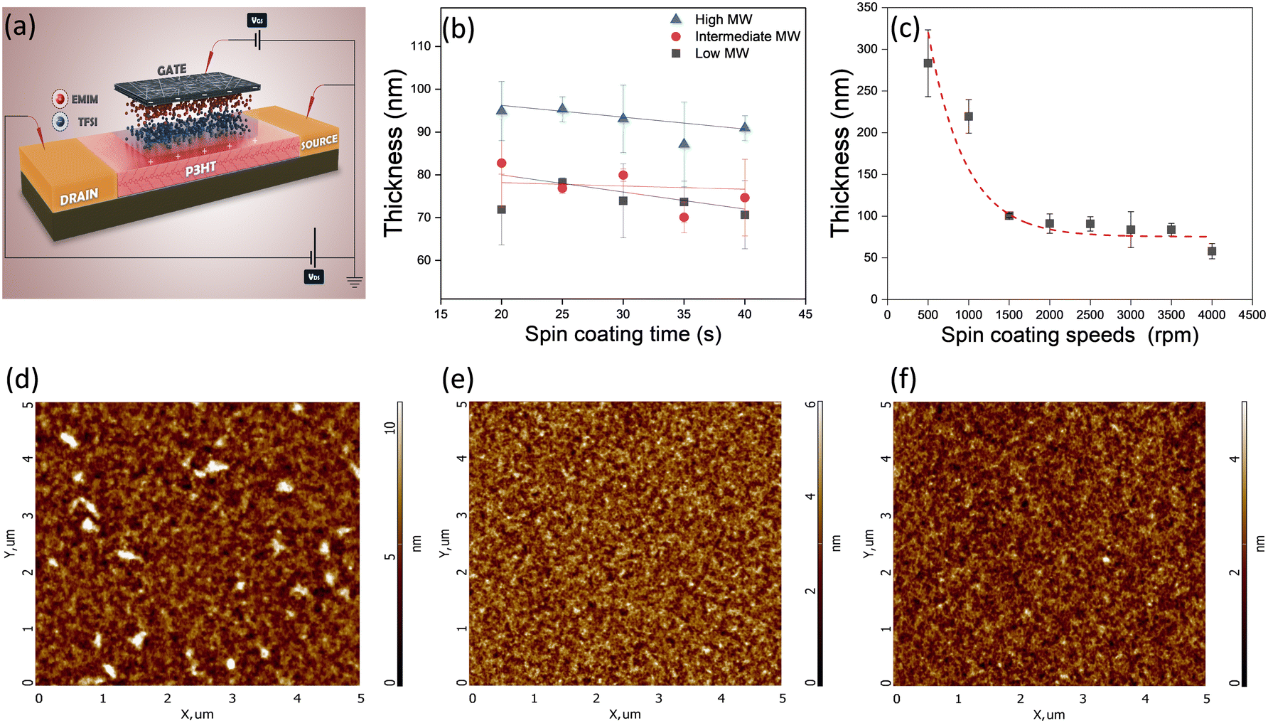 | ||
| Fig. 1 a) P3HT-based IGT device structure. Thickness of P3HT films deposited with: b) different MWs at five spin coating times (20, 25, 30, 35, and 40 s, at 1000 rpm), c) different spin coating speeds (lines are fittings) at 30 s and with MW 50–70 kDa. AFM images of P3HT films, spin coated during 30 s on SiO2/Si, at 1000 rpm, d) low MW e) intermediate MW f) high MW. Image size is 5 μm × 5 μm. | ||
Results and discussion
To study the effect of MW and thickness of P3HT thin films on the response time and synaptic behavior of IGTs, we spin coated P3HT films on SiO2/Si using different P3HT MWs (namely low (24 kDa), intermediate (42 kDa), and high (92 kDa)), different spin coating times from 20 to 40 s and different rotation speeds (500 rpm, 1000 rpm, 2000 rpm, 4000 rpm). We observe a difference in thickness among various MWs P3HT films and spin coating times (Fig. 1b).Increasing the spin-coating speed, we observe a decrease of the P3HT film thickness (Fig. 1c). AFM images of P3HT films (Fig. 1d–f) reveal that the root mean square (rms) roughness of the surface decreases with an increase in the molecular weight (MW) of P3HT, i.e. 2.2 ± 0.6 nm for low MW, 0.8 ± 0.1 nm for intermediate MW, and 0.60 ± 0.03 nm for high MW P3HT, for a spin-coating time of 30 s at 1000 rpm. In other words, the increase in the P3HT molecular weight is associated with an increase in the smoothness of the film surface, most likely due to an increase in the short-range order within the molecular weight.35–38
A. Effect of different P3HT MWs on response time and synaptic behavior of P3HT IGTs
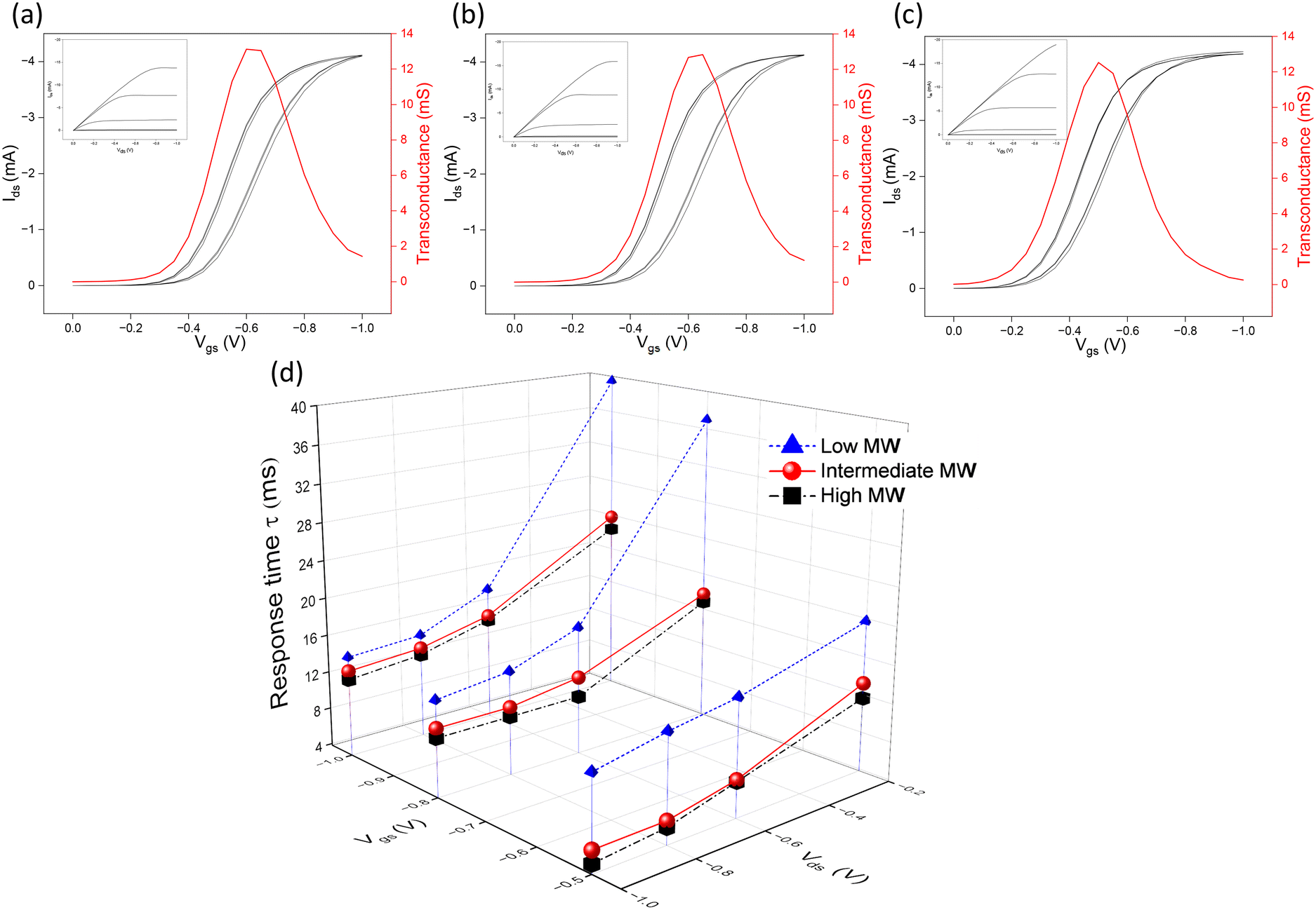 | ||
| Fig. 2 Transfer characteristics (black line) in the linear regime (Vds = −0.2 V, (3 cycles)) at Vgs scan rate 50 m V s−1 (inset: output characteristic with Vgs = 0, −0.2, −0.4, −0.6, −0.8, −1 V at Vds 50 m V s−1 scan rate) and transconductance curve (red line) for [EMIM][TFSI]-gated transistors based on a) high MW b) intermediate MW c) low MW P3HT deposited at 1000 rpm during 30 s. d) Transient response of an [EMIM] [TFSI]-gated P3HT transistor with high, intermediate, and low MW for Vgs = −1, −0.8, and −0.5 V at different Vds. The duration time of the Vgs bias is 200 ms. | ||
Devices fabricated using high MW P3HT exhibit a higher transconductance (gm = δIds/δVgs, a transistor parameter that describes how Ids responds to variations in Vgs (ref. 18 and 47)) than for low MW counterparts, attributable to higher ionic permeability.37,48,49 The increased transconductance implies that even a slight change in Vgs can result in a substantial variation in Ids, rendering high-MW P3HT IGTs more sensitive to changes in Vgs compared to lower MWs counterparts.
The response time increases with decreasing MW of P3HT, for Vgs = −0.5, −0.8, and −1 V (Fig. 2d). For instance, for pre-synaptic spikes with 200 ms pulse width, Vgs = −1 V and Vds = −0.2, τ increases from 22.3 to 39.5 ms, i.e. by 77%, with decreasing MW. The increase of MW brings about an increase in the entanglement of the P3HT chains, paralleled by an increase in the short-range ordered portion of the films.37,38,48 This is expected to promote ion permeability, i.e., facilitate P3HT doping/de-doping.
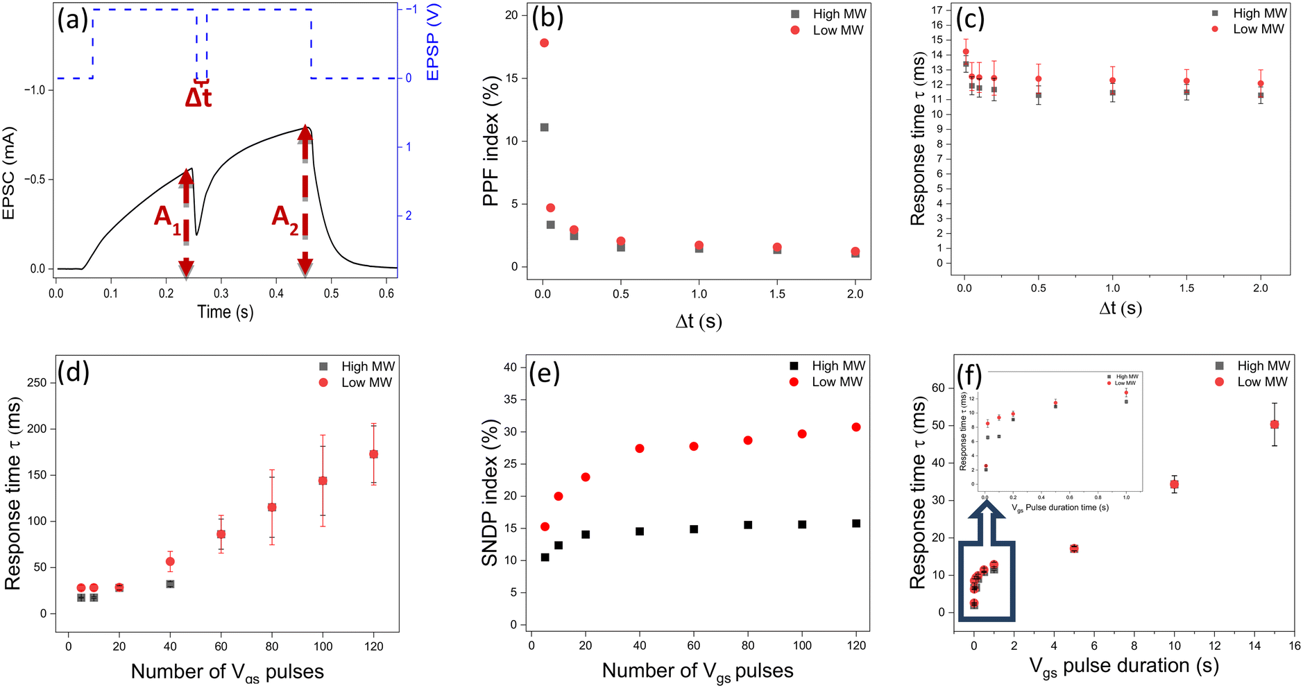 | ||
| Fig. 3 Synaptic behavior of artificial synapses based on P3HT IGTs for different P3HT MWs. a) Ids triggered by a pair of successive presynaptic Vgs (−1 V) pulses with a pulse interval Δt. A1 and A2 are the amplitudes of Ids. b) PPF index as a function of pulse interval of two consecutive Vgs pulses, Δt = 10 ms to 2 s. c) Response time of second Ids pulses after applying two consecutive Vgs pulses versus time interval of pulses, Δt. d) Response time of P3HT IGT versus different numbers of Vgs square step train pulses, from 5 to 120 pulses. Vgs = −1 V and Vds = −0.6 V. e) SNDP index as a function of the. number of Vgs pulses. f) Response time of IGT versus Vgs pulse duration for low and high MW P3HT. | ||
Increasing the degree of order (i.e. increasing the roughness) in the semiconducting channel by decreasing the P3HT MW brings about limited ion permeability over an extended lapse of time. A higher quantity of ions contributes to an elevated PPF index (Fig. 3b). The summation effect causes an increase in the IGT response time (Fig. 3c).
With the increase of n, there is an increase in ion redistribution time, paralleled by an increase of τ. We observed a significant impact of P3HT MW on the IGT response time when a low number of pulses was applied. However, as the number of pulses increased, τ of different P3HT MWs became nearly identical (Fig. 3d).
B. Impact of film thickness (as controlled by spin coating conditions) on response time and synaptic behavior in P3HT IGTs
IGT transfer (Vgs scan rate 100, 50 and 25 m V s−1, and Vds = −0.2 V) and output characteristics (Vds scan rate 100, 50 and 25 m V s−1, and Vgs = 0 to −1 V) show that Ids decreases with the increase of the spin coating speed (thinner P3HT film) (Fig. 4a–d, S2a-l† and 1c). The higher permeability of thinner P3HT channels due to the lower degree of order brings about higher transconductance, i.e. an enhanced IGT sensitivity to changes in Vgs.34,40,48,49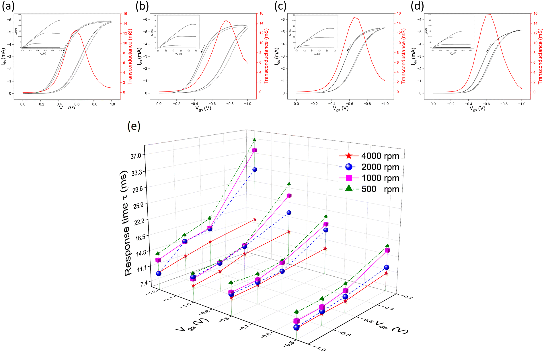 | ||
| Fig. 4 Transfer characteristics in the linear regime (Vds = −0.2 V (3 cycles)) at Vgs 50 m V s−1 scan rate (inset: output characteristic with Vgs = 0, −0.2, −0.4, −0.6, −0.8, −1 V and Vds 50 m V s−1 scan rate) and transconductance curve for [EMIM][TFSI]-gated P3HT transistors prepared with spin coating rate: a) 500 rpm b) 1000 rpm c) 2000 rpm d) 4000 rpm, on 30 seconds with intermediate MW. e) Transient response of [EMIM][TFSI]-gated P3HT transistors with intermediate MW with Vgs = −1.2, −1, −0.8, and −0.5 V, at different Vds. The duration of the Vgs bias is 200 ms. | ||
We investigated the response time of P3HT IGTs by employing a square Vgs pulse with a width of 200 ms and varied amplitudes of −0.5, −0.8, −1, and −1.2 V. The measurements were performed at different Vds of −0.2, −0.6, −8, and −1 V (Fig. 4e). Additionally, we examined the impact of different channel thicknesses (as determined by the spin coating rates used for P3HT films' deposition) on τ. The increase of τ with the increase of Vgs and the decrease of τ with the increase of Vds are clear for all spin coating speeds. Further, τ increases with the decrease of the spin coating speed from 4000 to 500 rpm (Fig. 4e). The increased order of P3HT obtained by decreasing spin coating speed decreases the permeability of ions into the channel and increases the ion redistribution time or IGT response time. We can also explain the observed result through the Bernards' model.27
Fig. 5a shows increasing film thickness can enhance the pair pulse facilitation. Slow ion diffusion in a thick channel affects pair pulse facilitation, possibly leading to longer facilitation times (Fig. 5b). With thick films, the channel can store more charge upon the first pulse, leading to more pronounced facilitation during the second pulse.
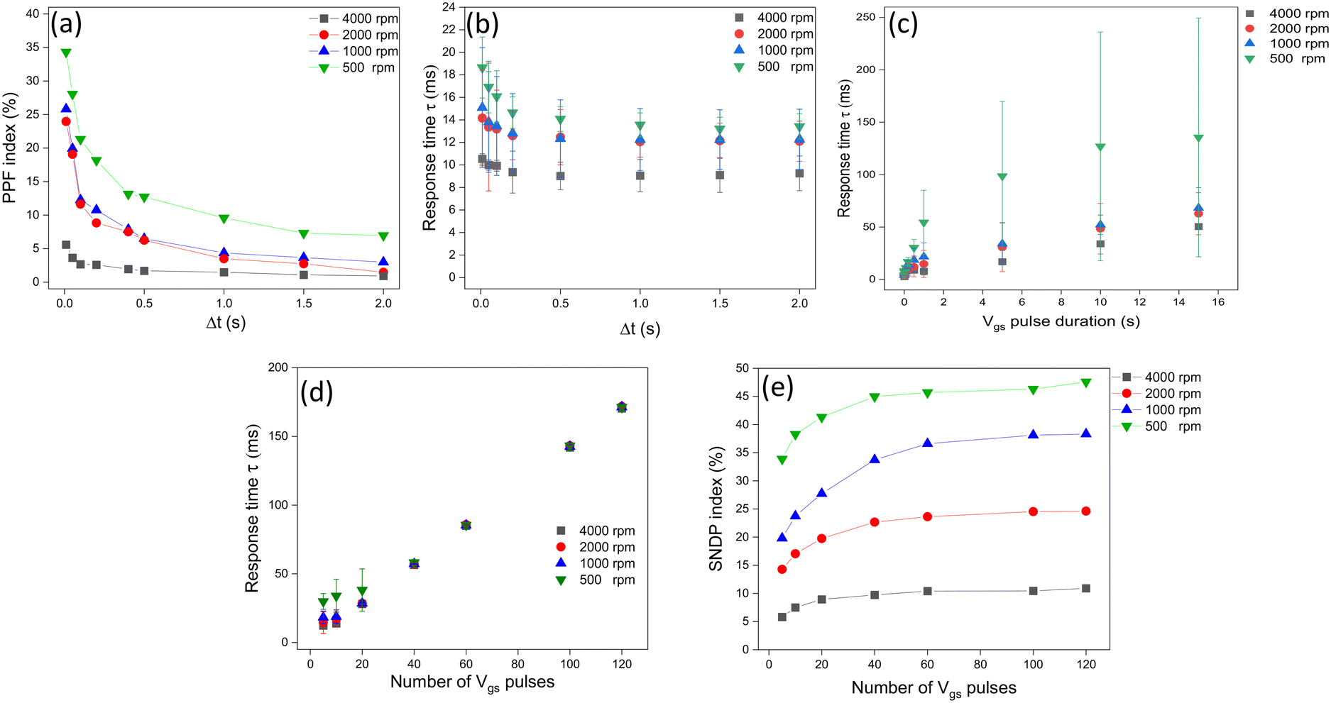 | ||
| Fig. 5 Synaptic behavior of artificial synapses based on P3HT IGTs for films spin coated at different speeds (in turn associated with thicknesses, Fig. 1c). a) PPF index as a function of pulse interval of two consecutive Vgs pulses (Δt from 10 ms to 2 s). b) Response time of second Ids pulses after applying two consecutive Vgs pulses versus time interval of pulses (Δt). c) Response time of IGTs versus Vgs pulse duration. d) Response time of P3HT IGTs versus different numbers of Vgs square step train pulses, from 5 to 120 pulses. Vgs = −1 V and Vds = −0.6 V. e) SNDP index ((An − A1)/A1 × 100%), with n = the number of Vgs pulses, as a function of the number of Vgs pulses. | ||
Fig. 5c and d show that the increase of the Vgs pulse duration time and number of pulses can have the same effect on the synaptic behavior of P3HT IGTs with different channel thicknesses (obtained by controlling the spin coating conditions as detailed in Fig. 1c). By increasing the number of pulses and Vgs pulse duration, we can increase τ, which can be interpreted as the redistribution time of the ions, upon Vgs removal. Increasing the thickness (going from a spin coating speed of 4000 rpm to 500 rpm, Fig. 1c) results in an increase in τ for all Vgs pulse duration times and pulse numbers (Fig. 5c and d).
Further, we can observe a stronger transition from STP to LTP, in a thicker P3HT film. We observed that SNDP1−120 (where SNDP1−n = (An − A1)/A1 × 100%) is 48% for thick channel films (500 rpm) and 11% for thin films (4000 rpm). These values quantitatively describe the evolution of the SNDP index with the thickness of the P3HT films (Fig. 5e and 1e).
Experimental
A. Microfabrication
Photolithography for electrode patterning was performed on 200 ± 10 nm-thick SiO2 on 525 ± 25 μm-thick doped silicon wafer purchased from WaferPro, San Jose, California. Au/Ti electrodes (40 nm/5 nm) had a width (W) of 4 mm and an interelectrode distance (L) of 10 μm. The patterned substrates were cleaned with a sequential ultrasonic bath in isopropanol alcohol (IPA) for 10 min, acetone for 10 min and IPA for 10 min, prior to the deposition of the P3HT thin films.B. P3HT films deposition
P3HT solutions consisting of 10 mg regioregular P3HT (RIEKE Metals) with different molecular weights, low (24 kDa), intermediate (42 kDa), and high (92 kDa), in 1 ml chlorobenzene were stirred overnight in an N2 glove box (O2 < 5 ppm, H2O < 5 ppm). P3HT films were deposited by 30 seconds spin coating at 1000 rpm on the SiO2/Si substrates. In order to control the thickness of the films, P3HT with MW 50–70 kDa were spin coated for 30 seconds at various rotation speeds: 500, 1000, 2000, and 4000 rpm. All devices were thermally treated on a hotplate at 100 °C for 2 h in the N2 glovebox. The ionic liquid used as the gating medium, [EMIM][TFSI], purchased from IoLiTec (>99%), was purified under vacuum (ca. 10−5 Torr) for 24 h at 60 °C before use. [EMIM][TFSI] was dropped onto the Durapore® membrane (4 mm × 9 mm-sized, 125 μm-thick). The membrane was positioned in correspondence with the transistor channel. Large surface area carbon paper (Spectracarb 2050, 170 μm-thick), coated with an ink comprising activated carbon (PICACTIF SUPERCAP BP10, Pica, 28 mg ml−1) and polyvinylidene fluoride (PVDF, KYNAR HSV900, 1.4 mg ml−1) binder in N-methyl pyrrolidone (NMP, Fluka) was utilized as the gate electrode (6 mm × 3 mm-sized).C. Characterization of the channel material
The thickness of P3HT thin films were measured by Dektak 150 profilometer. To obtain the thin film height, the probe physically moved along the surface during the measurement. The topography of the samples was probed by atomic force microscopy (AFM), in ambient conditions, with an NT-MDT NTEGRA II microscope. The images were acquired in semi-contact (tapping) mode with an NSG10 cantilever (a length of 95 um, a width of 30 um, resonant frequency of 240 kHz and force constant of 11.8 N m−1).D. Electrical characterization of the devices
Transistor characterization was conducted using a semiconductor parameter analyzer, Agilent B1500A, and a house-made micromanipulated electrical probe station inside the N2 glove box.Conclusions
In conclusion, we conducted a comprehensive study of the properties and performance of synaptic P3HT ion-gated transistors (IGTs). We examined the effect of P3HT molecular weight (MW) on morphology, transistor device characteristics, response time, and synaptic behavior of IGTs fabricated with low (24 kDa), intermediate (42 kDa), and high (92 kDa) MW. Low MW P3HT films, exhibiting a higher degree of order, expected to be associated to lower ion permeability with respect to intermediate and high MW P3HT films, bringing about corresponding devices with lower transconductance. Further, low MW P3HT IGTs exhibit longer response times upon application of Vgs pulses concerning counterparts making use of intermediate and high MW.We emulated several essential synaptic functions, including PPF and SNDP, and realized a transition from STP to LTP by tuning Vgs pulses' parameters, such as amplitude, duration, and pulses' number, in low, intermediate, and high MW P3HT-IGTs. In all cases, devices with low MW P3HT have more effective STP-to-LTP transition than medium and high MW counterparts.
The study of the dependence of response time and synaptic behavior on film thickness in P3HT-based IGTs revealed that films deposited with lower spin coating speeds (thicker films, more ordered films) feature lower transconductance. Our study demonstrates a significant increase in the response time of IGTs with an increasing thickness of the P3HT film. Moreover, increasing film thickness brings about an improvement in synaptic behavior, encompassing PPF and SNDP. The transition from STP to LTP is achieved by controlling the thickness of the films. Thicker P3HT films bring about higher levels of LTP.
In perspective, we plan to explore the development of organic synaptic phototransistors exposed to light pulses, to finely tune and modulate synaptic behaviors.
Author contributions
R. K. A. and C. S. designed the experiments. R. K. A. and Z. G. performed the transistor and time-resolved characterizations. R. K. A and A. C. performed AFM experiments. R. K. A., Z. G. and C. S. drafted the manuscript. All authors commented on the manuscript.Conflicts of interest
There are no conflicts to declare.Acknowledgements
C. S. acknowledges NSERC (Discovery Grant) for financial support.References
- C. D. Schuman, S. R. Kulkarni, M. Parsa, J. P. Mitchell, P. Date and B. Kay, Opportunities for neuromorphic computing algorithms and applications, Nat. Comput. Sci., 2022, 2(1), 10–19 CrossRef PubMed.
- K. Sun, J. Chen and X. Yan, The Future of Memristors: Materials Engineering and Neural Networks, Adv. Funct. Mater., 2021, 31(8), 2006773 CrossRef CAS.
- Y. Zhang, P. Qu, Y. Ji, W. Zhang, G. Gao, G. Wang, S. Song, G. Li, W. Chen, W. Zheng, F. Chen, J. Pei, R. Zhao, M. Zhao and L. Shi, A system hierarchy for brain-inspired computing, Nature, 2020, 586(7829), 378–384 CrossRef CAS PubMed.
- X. Zou, S. Xu, X. Chen, L. Yan and Y. Han, Breaking the von Neumann bottleneck: architecture-level processing-in-memory technology, Sci. China Inf. Sci., 2021, 64(6), 160404 CrossRef.
- Y. Yang, P. Gao, S. Gaba, T. Chang, X. Pan and W. Lu, Observation of conducting filament growth in nanoscale resistive memories, Nat. Commun., 2012, 3(1), 732 CrossRef PubMed.
- Y. Yang, X. Zhang, L. Qin, Q. Zeng, X. Qiu and R. Huang, Probing nanoscale oxygen ion motion in memristive systems, Nat. Commun., 2017, 8(1), 15173 CrossRef PubMed.
- A. Wedig, M. Luebben, D.-Y. Cho, M. Moors, K. Skaja, V. Rana, T. Hasegawa, K. K. Adepalli, B. Yildiz and R. Waser, Nanoscale cation motion in TaO x, HfO x and TiO x memristive systems, Nat. Nanotechnol., 2016, 11(1), 67–74 CrossRef CAS PubMed.
- P. Sheridan, F. Cai, C. Du, W. Ma, Z. Zhang and W. D. Lu, Sparse coding with memristor networks, Nat. Nanotechnol., 2017, 12, 784–789 CrossRef CAS PubMed.
- P. Yao, H. Wu, B. Gao, S. B. Eryilmaz, X. Huang, W. Zhang, Q. Zhang, N. Deng, L. Shi and H.-S. P. Wong, Face classification using electronic synapses, Nat. Commun., 2017, 8(1), 15199 CrossRef CAS PubMed.
- C. Li, M. Hu, Y. Li, H. Jiang, N. Ge, E. Montgomery, J. Zhang, W. Song, N. Dávila and C. E. Graves, Analogue signal and image processing with large memristor crossbars, Nat. Electron., 2018, 1(1), 52–59 CrossRef.
- S. Kim, C. Du, P. Sheridan, W. Ma, S. Choi and W. D. Lu, Experimental demonstration of a second-order memristor and its ability to biorealistically implement synaptic plasticity, Nano Lett., 2015, 15(3), 2203–2211 CrossRef CAS PubMed.
- P. Monalisha, A. P. Kumar, X. R. Wang and S. Piramanayagam, Emulation of Synaptic Plasticity on a Cobalt-Based Synaptic Transistor for Neuromorphic Computing, ACS Appl. Mater. Interfaces, 2022, 14(9), 11864–11872 CrossRef CAS PubMed.
- S. Yamamoto, A. G. Polyravas, S. Han and G. G. Malliaras, Correlation between Transient Response and Neuromorphic Behavior in Organic Electrochemical Transistors, Adv. Electron. Mater., 2022, 8(4), 2101186 CrossRef CAS.
- J. Y. Gerasimov, R. Gabrielsson, R. Forchheimer, E. Stavrinidou, D. T. Simon, M. Berggren and S. Fabiano, An Evolvable Organic Electrochemical Transistor for Neuromorphic Applications, Adv. Sci., 2019, 6(7), 1801339 CrossRef PubMed.
- J. Y. Gerasimov, D. Zhao, A. Sultana, T. Abrahamsson, S. Han, D. Bliman, D. Tu, D. T. Simon, R. Olsson, X. Crispin, M. Berggren and S. Fabiano, A Biomimetic Evolvable Organic Electrochemical Transistor, Adv. Electron. Mater., 2021, 7(11), 2001126 CrossRef CAS.
- Y.-T. Yang, H.-C. Tien, C.-C. Chueh and W.-Y. Lee, Polymer synaptic transistors from memory to neuromorphic computing, Mater. Chem. Phys., 2022, 287, 126263 CrossRef CAS.
- Z. Wang, L. Wang, Y. Wu, L. Bian, M. Nagai, R. Jv, L. Xie, H. Ling, Q. Li, H. Bian, M. Yi, N. Shi, X. Liu and W. Huang, Signal Filtering Enabled by Spike Voltage-Dependent Plasticity in Metalloporphyrin-Based Memristors, Adv. Mater., 2021, 33(43), 2104370 CrossRef CAS PubMed.
- J. Rivnay, S. Inal, A. Salleo, R. M. Owens, M. Berggren and G. G. Malliaras, Organic electrochemical transistors, Nat. Rev. Mater., 2018, 3(2), 1–14 Search PubMed.
- P. Hapiot and C. Lagrost, Electrochemical reactivity in room-temperature ionic liquids, Chem. Rev., 2008, 108(7), 2238–2264 CrossRef CAS PubMed.
- A. Laiho, L. Herlogsson, R. Forchheimer, X. Crispin and M. Berggren, Controlling the dimensionality of charge transport in organic thin-film transistors, Proc. Natl. Acad. Sci. U. S. A., 2011, 108(37), 15069–15073 CrossRef CAS PubMed.
- M. Zakrewsky, K. S. Lovejoy, T. L. Kern, T. E. Miller, V. Le, A. Nagy, A. M. Goumas, R. S. Iyer, R. E. Del Sesto and A. T. Koppisch, Ionic liquids as a class of materials for transdermal delivery and pathogen neutralization, Proc. Natl. Acad. Sci. U. S. A., 2014, 111(37), 13313–13318 CrossRef CAS PubMed.
- G.-T. Go, Y. Lee, D.-G. Seo, M. Pei, W. Lee, H. Yang and T.-W. Lee, Achieving microstructure-controlled synaptic plasticity and long-term retention in ion-gel-gated organic synaptic transistors, Adv. Intell. Syst., 2020, 2(11), 2000012 CrossRef.
- S. Wang, X. Chen, C. Zhao, Y. Kong, B. Lin, Y. Wu, Z. Bi, Z. Xuan, T. Li and Y. Li, An organic electrochemical transistor for multi-modal sensing, memory and processing, Nat. Electron., 2023, 6(4), 281–291 CrossRef CAS.
- R. Karimi Azari, T. Lan and C. Santato, On the factors affecting the response time of synaptic ion-gated transistors, J. Mater. Chem. C, 2023, 11(24), 8293–8299 RSC.
- R. S. Zucker and W. G. Regehr, Short-term synaptic plasticity, Annu. Rev. Physiol., 2002, 64(1), 355–405 CrossRef CAS.
- D. E. Clapham, Calcium signaling, Cell, 2007, 131(6), 1047–1058 CrossRef CAS PubMed.
- D. A. Bernards and G. G. Malliaras, Steady-State and Transient Behavior of Organic Electrochemical Transistors, Adv. Funct. Mater., 2007, 17(17), 3538–3544 CrossRef CAS.
- N. M. B. Neto, M. D. Silva, P. T. Araujo and R. N. Sampaio, Photoinduced Self-Assembled Nanostructures and Permanent Polaron Formation in Regioregular Poly (3-hexylthiophene), Adv. Mater., 2018, 30(16), 1705052 CrossRef PubMed.
- Z. Chiguvare and J. Parisi, Current conduction in poly (3-Hexylthiophene) and in poly (3-hexylthiophene) doped [6, 6]-phenyl C61-butyric acid methylester composite thin film devices, Z. Naturforsch., A: Phys. Sci., 2012, 67(10–11), 589–600 CrossRef CAS.
- A. Nawaz, A. Kumar and I. A. Hümmelgen, Ultra-high mobility in defect-free poly (3-hexylthiophene-2, 5-diyl) field-effect transistors through supra-molecular alignment, Org. Electron., 2017, 51, 94–102 CrossRef CAS.
- A. Salleo, Charge transport in polymeric transistors, Mater. Today, 2007, 10(3), 38–45 CrossRef CAS.
- L. Hrostea, M. Girtan, R. Mallet and L. Leontie, in Optical and morphological properties of P3HT and P3HT: PCBM thin films used in photovoltaic applications, IOP Conference Series: Materials Science and Engineering, IOP Publishing, 2018, p. 012015 Search PubMed.
- N. E. Persson, P.-H. Chu, M. McBride, M. Grover and E. Reichmanis, Nucleation, growth, and alignment of poly (3-hexylthiophene) nanofibers for high-performance OFETs, Acc. Chem. Res., 2017, 50(4), 932–942 CrossRef CAS PubMed.
- R. J. Kline, M. D. McGehee, E. N. Kadnikova, J. Liu and J. M. J. Fréchet, Controlling the Field-Effect Mobility of Regioregular Polythiophene by Changing the Molecular Weight, Adv. Mater., 2003, 15(18), 1519–1522 CrossRef CAS.
- C. Goh, R. J. Kline, M. D. McGehee, E. N. Kadnikova and J. M. Fréchet, Molecular-weight-dependent mobilities in regioregular poly (3-hexyl-thiophene) diodes, Appl. Phys. Lett., 2005, 86(12), 122110 CrossRef.
- O. G. Reid, J. A. N. Malik, G. Latini, S. Dayal, N. Kopidakis, C. Silva, N. Stingelin and G. Rumbles, The influence of solid-state microstructure on the origin and yield of long-lived photogenerated charge in neat semiconducting polymers, J. Polym. Sci., Part B: Polym. Phys., 2012, 50(1), 27–37 CrossRef CAS.
- A. G. Dixon, R. Visvanathan, N. A. Clark, N. Stingelin, N. Kopidakis and S. E. Shaheen, Molecular weight dependence of carrier mobility and recombination rate in neat P3HT films, J. Polym. Sci., Part B: Polym. Phys., 2018, 56(1), 31–35 CrossRef CAS.
- R. Noriega, J. Rivnay, K. Vandewal, F. P. Koch, N. Stingelin, P. Smith, M. F. Toney and A. Salleo, A general relationship between disorder, aggregation and charge transport in conjugated polymers, Nat. Mater., 2013, 12(11), 1038–1044 CrossRef CAS PubMed.
- H. Yang, T. Joo Shin, Z. Bao and C. Y. Ryu, Structural transitions of nanocrystalline domains in regioregular poly (3-hexyl thiophene) thin films, J. Polym. Sci., Part B: Polym. Phys., 2007, 45(11), 1303–1312 CrossRef CAS.
- L. H. Jimison, S. Himmelberger, D. T. Duong, J. Rivnay, M. F. Toney and A. Salleo, Vertical confinement and interface effects on the microstructure and charge transport of P3HT thin films, J. Polym. Sci., Part B: Polym. Phys., 2013, 51(7), 611–620 CrossRef CAS.
- S. Joshi, S. Grigorian and U. Pietsch, X-ray structural and crystallinity studies of low and high molecular weight poly (3-hexylthiophene), Phys. Status Solidi A, 2008, 205(3), 488–496 CrossRef CAS.
- W. Porzio, G. Scavia, L. Barba, G. Arrighetti and S. Milita, Depth-resolved molecular structure and orientation of polymer thin films by synchrotron X-ray diffraction, Eur. Polym. J., 2011, 47(3), 273–283 CrossRef CAS.
- S. Joshi, S. Grigorian, U. Pietsch, P. Pingel, A. Zen, D. Neher and U. Scherf, Thickness dependence of the crystalline structure and hole mobility in thin films of low molecular weight poly (3-hexylthiophene), Macromolecules, 2008, 41(18), 6800–6808 CrossRef CAS.
- J. H. Cho, J. Lee, Y. He, B. S. Kim, T. P. Lodge and C. D. Frisbie, High-Capacitance Ion Gel Gate Dielectrics with Faster Polarization Response Times for Organic Thin Film Transistors, Adv. Mater., 2008, 20(4), 686–690 CrossRef CAS.
- G. D. Spyropoulos, J. N. Gelinas and D. Khodagholy, Internal ion-gated organic electrochemical transistor: A building block for integrated bioelectronics, Sci. Adv., 2019, 5(2), eaau7378 CrossRef CAS PubMed.
- D. Rawlings, E. M. Thomas, R. A. Segalman and M. L. Chabinyc, Controlling the Doping Mechanism in Poly(3-hexylthiophene) Thin-Film Transistors with Polymeric Ionic Liquid Dielectrics, Chem. Mater., 2019, 31(21), 8820–8829 CrossRef CAS.
- J. Rivnay, P. Leleux, M. Ferro, M. Sessolo, A. Williamson, D. A. Koutsouras, D. Khodagholy, M. Ramuz, X. Strakosas, R. M. Owens, C. Benar, J.-M. Badier, C. Bernard and G. G. Malliaras, High-performance transistors for bioelectronics through tuning of channel thickness, Sci. Adv., 2015, 1(4), e1400251 CrossRef PubMed.
- A. M. Ballantyne, L. Chen, J. Dane, T. Hammant, F. M. Braun, M. Heeney, W. Duffy, I. McCulloch, D. D. C. Bradley and J. Nelson, The Effect of Poly(3-hexylthiophene) Molecular Weight on Charge Transport and the Performance of Polymer:Fullerene Solar Cells, Adv. Funct. Mater., 2008, 18(16), 2373–2380 CrossRef CAS.
- T. Lan, Z. Gao, M. S. Barbosa and C. Santato, Flexible ion-gated transistors making use of poly-3-hexylthiophene (P3HT): effect of the molecular weight on the effectiveness of gating and device performance, J. Electron. Mater., 2020, 49, 5302–5307 CrossRef CAS.
Footnote |
| † Electronic supplementary information (ESI) available. See DOI: https://doi.org/10.1039/d4lf00003j |
| This journal is © The Royal Society of Chemistry 2024 |