
 Open Access Article
 This Open Access Article is licensed under a
 Creative Commons Attribution 3.0 Unported Licence
Microfluidic-organic thin film transistor coupled platform for simple solution exposure†
Nicholas T.
Boileau
a,
Benjamin
King
a,
Sparsh
Kapar
a,
Ali Najafi
Sohi
b,
Joseph G.
Manion
a,
Michel
Godin
 bc and
Benoît H.
Lessard
*ad
bc and
Benoît H.
Lessard
*ad
aDepartment of Chemical and Biological Engineering, University of Ottawa, 161 Louis Pasteur Pvt, Ottawa, ON, Canada. E-mail: benoit.lessard@uottawa.ca
bDepartment of Physics, University of Ottawa, 150 Louis Pasteur Pvt, Ottawa, ON, Canada
cOttawa-Carleton Institute for Biomedical Engineering, University of Ottawa, 161 Louis Pasteur Pvt, Ottawa, ON, Canada
dSchool of Electrical Engineering and Computer Science, University of Ottawa, 800 King Edward Ave., Ottawa, ON, Canada
First published on 28th March 2024
Abstract
Efforts to combine organic thin film transistors (OTFTs) within microfluidic networks to create sensitive, versatile, and low-cost sensors for rapid chemical analysis have been limited by the need for complex equipment and by the sensitivity of OTFTs to common processing techniques used in traditional microfluidic fabrication. We designed and validated a robust, easy to use, and simple to manufacture prototype microfluidic–OTFT pressure coupled system. Our design enables multiple OTFT architectures to be combined with microfluidic analyte delivery, eliminates common processing steps that can alter OTFT performance, and only requires easily-accessible equipment. As a proof of concept, we demonstrate the exposure of aluminium chloride phthalocyanine (AlClPc) based OTFTs to different solutions of sodium fluoride (NaF). This work could accelerate the design of more versatile, rapid, and reliable OTFT based liquid chemical sensors.
Introduction
Fast, sensitive, and selective sensor devices that replace or augment laboratory testing show great promise for improving manufacturing,1 environmental monitoring,2 and personalized medicine3 by enabling real-time data capture. Often, electrochemical or colorimetric devices have been used in these applications, including in devices such as hazardous gas sensors, sweat monitors, heavy metal sensors, and in situ small molecule sensors.4–9 While effective, these devices may sometimes lack sensitivity and specificity, and therefore recent interest has focused on using an organic thin film transistor (OTFT) as the sensing element. OTFT devices have shown great potential as inexpensive, versatile, and sensitive point-of-use chemical sensors.10–13 Various OTFT architectures have been used to successfully construct biosensors for common analytes such as glucose,14 DNA,15 assorted proteins,16–21 and many others.22 The use of organic semiconductors can also introduce unique interactions and sensing mechanisms to analytes such as the specific film restructuring of phthalocyanines with exposure to cannabinoids.23–27 To date, the majority of reported OTFT sensors rely on manual deposition of analyte solutions, typically using micropipettes.28,29 Though manual droplet dispensing can be convenient for single devices, it is not a scalable process for high-throughput testing, prevents continuous analysis, and has been shown to introduce significant run-to-run variation, limiting reproducibility.30 Successful scale-up of drop-casting type protocols requires expensive precision instruments capable of in situ deposition and testing to ensure that droplets are placed consistently and tested within narrow time constraints to prevent droplet evaporation or sample degradation.Microfluidic platforms eliminate several issues inherent to droplet-based operation of OTFT sensors31 and offer a variety of advantages over traditional methods, including multiplexing, low sample volume consumption, and high throughput.32 Microfluidics have also been successfully combined with a variety of devices including nanopore based sensors,33 pressure sensors,34 optical sensors,35 and electrochemical sensors.36 Methods to fabricate such sensor-microfluidic devices include using soft lithography, lamination techniques, and even 3D printing.37 Typically for more traditional sensor and biosensor devices these methods are effective and low-cost but unfortunately the are detrimental to the integration of OTFTs due to the incompatible manufacturing steps. Specifically, rinsing of substrates with organic solvents, oxygen plasma treatment, and the use of adhesive compounds to bond microfluidic components to substrates are major roadblocks for integration with OTFTs.38 They may also require equipment or facilities that researchers interested in OTFTs and material characterization may not have access to, such as mask aligners and photolithography equipment. Consequently, few OTFTs have been integrated with microfluidics to date.39–44 Of these limited examples, the majority consist of electrolyte gated systems or systems with extended gate electrodes where the delicate organic semiconductor is not exposed to the microfluidic system/fabrication. The couple examples that expose the organic semiconductor to the microfluidic system employ expensive/complex lithography processes or use the deposition of a fluorochemical coating to create water guides, but lacks self containment. In this work we develop a simple, robust, and reliable method that uses a compressive clamping force to integrate microfluidics and OTFTs without the need for using adhesive, aligner equipment, or plasma surface treatment. This simplified assembly enables the use of sensitive semiconductors which would be destroyed with typical microfluidic device fabrication procedures.
To demonstrate the capabilities of this microfluidic–OTFT system we designed a simple fluoride salt sensor. Fluoride is often injected into drinking water to help prevent dental cavities but at high levels it can lead to poor health outcomes including gastroenteritis, neurological damage, cancer, infertility, and other diseases.45–48 According to the World Health Organization, acceptable fluoride levels fall below 1.5 ppm,49 however these levels are often surpassed due to groundwater pollution from improper industrial waste disposal and sewage.50–52 Industrial processes such as aluminium smelting and phosphate fertilizer manufacturing can have fluoride effluent concentrations up to 410 ppm.53 Furthermore, the majority of current fluoride sensors rely on fluorescent probes that require expensive analytical equipment.54–57 There has been some interest in using OTFT devices for fluoride detection. T. Minami et al. developed an extended gate OTFT system and saw positive threshold voltage shifts with increasing fluoride ion concentration at the gate electrode.58 JHL Ngai et al. developed an electrolyte gate OFET (EGOFET) using indigo polymer semiconductors to detect halide ions and saw decreasing current with increasing halide concentration as it was injected into the water based dielectric.59 Our proof-of-concept system was sensitive to fluoride using chloro aluminum phthalocyanine (AlClPc)-based OTFT sensors fed by microfluidic channels where the analyte directly interacted at the analyte–semiconductor interface rather than in the dielectric or at the electrodes which facilitates fluid interactions with the OTFTS.
Results and discussion
Design of easy-to-use and reproducible OTFT microfluidic platform
Existing OTFT sensors where analyte solutions are manually dispensed onto the sensor require restrictive designs for organic semiconductors and/or device architectures which can limit performance. If the semiconductor layer acts as the sensing element, it must be designed to preserve sensing capability while enabling orthogonal solvent processing to limit delamination or damage to the semiconductor film when exposed to analyte solutions. Similarly, device architectures that shield sensitive components such as electrodes and interlayers may be required to ensure adequate sensor performance. Microfluidic delivery of analytes may reduce exposure time of sensitive components, keep analytes restricted to the sensing element, and improve experimental flexibility, but requires compatibility with traditional methods that are destructive to many OTFTs. These typical methods include surface activation, chemical gluing, and adhesive based techniques, all of which significantly alter the organic semiconductor layer.60 Incompatibilities can also lead to poor adhesion of the microfluidic delivery system resulting in leakage that adversely impacts sensor reliability and lifetime. There have been efforts to address these concerns, but the proposed process requires heavily customized and complex photolithography and relies on water-soluble pattern transfer layers.61 To overcome these challenges, our system uses a pressure-based coupling strategy comprised of a four-part sandwich structure that secures an OTFT sensor between a guiding back and front plates and a microfluidic block. The pressure assembly can be quickly and easily set up, allows for integration of different substrates and OTFT architectures with microfluidic arrays, and circumvents surface treatments or chemical bonding of the microfluidic channels to the OTFT substrate (Fig. 1). This flexibility only requires the user to design OTFTs within the constraints set by the mounting components, which can themselves be adjusted and fabricated with standard drafting software and access to 3D printing or a machine shop.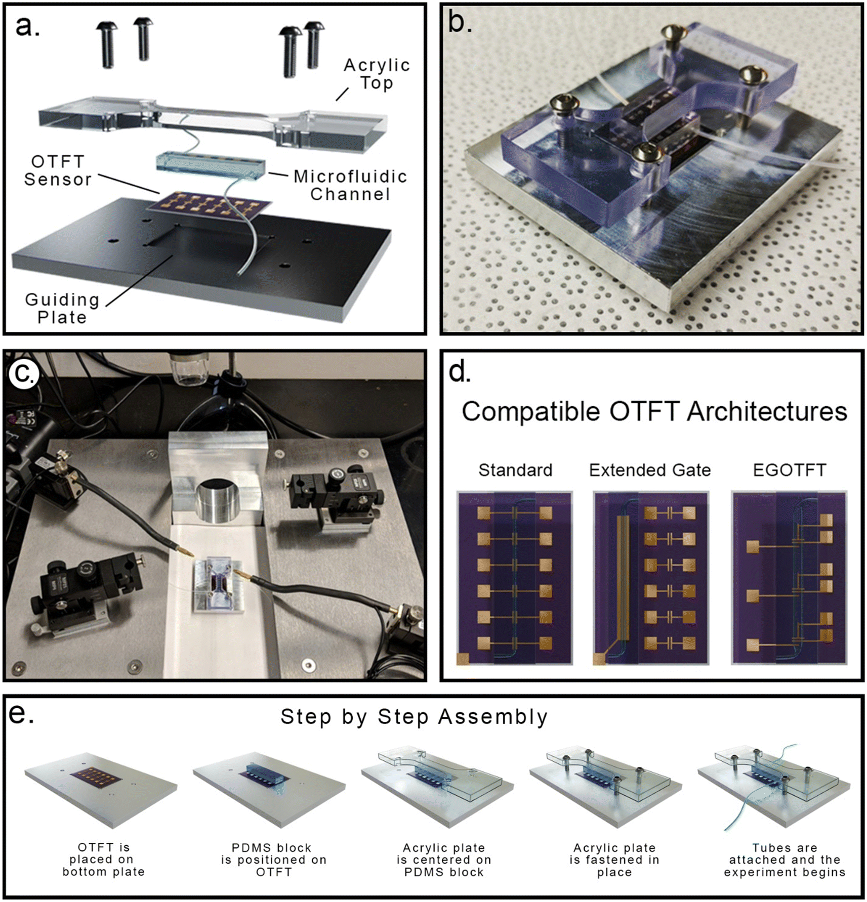 | ||
| Fig. 1 Microfluidic OTFT pressure coupling system. (a) Schematic overview of the system components, (b) the assembled system with an OTFT, (c) assembled setup ready for testing. d. Examples of compatible OTFT architectures (e) step by step assembly of the experimental setup. | ||
Expanding platform capabilities using electronically controlled fluid dispensation
Our initial prototype system used direct injection of analyte solutions into the microfluidic channel with a simple disposable syringe. This allowed the solution to be mixed and characterized prior to injection into the channel, where it then fills the channel, and remains at rest until the OTFT measurement is complete. While straightforward this approach only enabled introduction of one fluid, for a single point in time measurement. For improved robustness and method customizability, an electronically controlled pressure-based system was explored for introducing analytes, mixing solutions, and adjusting flow parameter controls. In this work a modified version of the system reported by Godin and coworkers was used.62 Additional details can be found in the Experimental section. This enables a user to control flow rate and analyte injection over time, wash or rinse devices, and introduce new analytes during analysis. Precise control of sample flow is a key factor in optimizing response time, sensitivity, selectivity and sample volume minimization of the microfluidic systems.63Proof of concept: chloroaluminum phthalocyanine (AlClPc) OTFTs with exposure to NaF containing aqueous solutions
To evaluate the viability of our pressure-coupled system, we fabricated AlClPc (Fig. 2A) OTFT combined with microfluidic, followed by the exposure of aqueous solutions containing sodium fluoride (NaF) in the range of 0 ppm to 100 ppm NaF. AlClPc devices were fabricated in a bottom gate bottom contact configuration (Fig. 2B) as detailed in the methods section. OTFTs were characterized with water flowing through the microfluidics system, in air at 20 °C. After integration with the microfluidics system, the OTFTs were characterized either dry (in air, 20 °C), or with the flow of distilled water through the channel at 20 °C. Representative transfer curves for each liquid analyte condition are shown in Fig. 2C. Each condition was tested with an individual chip comprising 6 devices. OTFTs initially characterized before integration achieved an average mobility of 6.6 ± 0.1 × 10⁻² cm2 V−1 s−1 (number of devices = 6). After assembly into the microfluidic system, a decrease of 3.5 ± 0.1 × 10⁻² cm2 V−1 s−1 in mobility was observed, followed by a further decrease of 2.4 ± 0.2 × 10⁻² cm2 V−1 s−1 after the introduction of distilled water through the channel. IOn/Off remained within the same order of magnitude across treatments, and there was a small positive ΔVT shift (+2.08 V). These results highlight that our simple microfluidic setup has a small and predictable impact on bottom gate bottom contact OTFTs with an AlClPc organic semiconductor. Following baseline tests, each of the aqueous solutions of NaF at various concentrations were introduced across an individual OTFT chip/microfluidic assembly with 6 transistors per substrate, identical to the “standard” architecture in Fig. 1d. Significant positive shifts in VT were observed with increasing concentrations of NaF within the tested range (Fig. 2D) suggesting that the OTFT could detect changes in concentration of analytes in this microfluidic delivery system.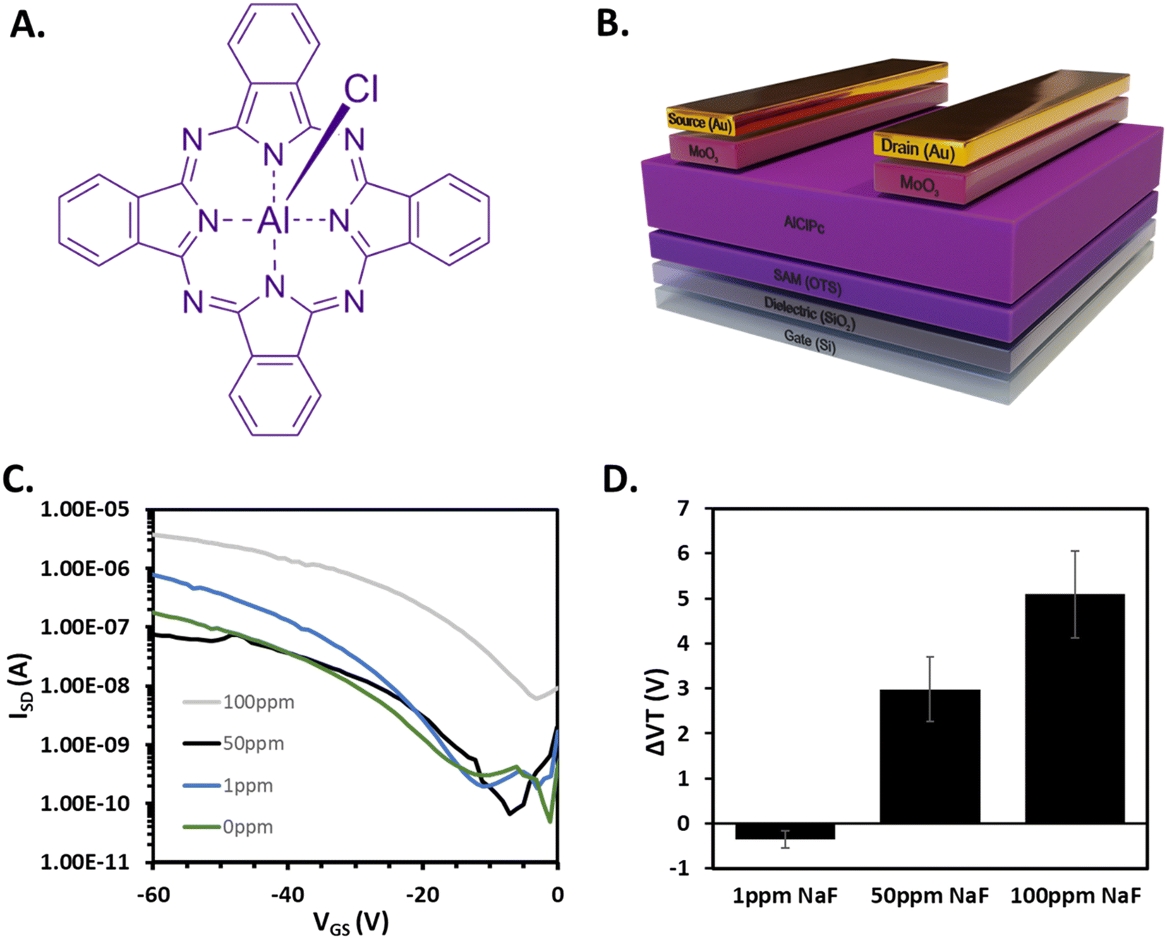 | ||
| Fig. 2 Device characteristics and sensor performance. (A) Chemical structure of AlClPc. (B) AlClPc BGTC device structure. (C) AlClPc OTFT transfer curves after assembly into PDMS system and after introduction of water based NaF samples at 0, 1, 50, or 100 ppm. (D) Threshold voltage change with NaF introduction to AlClPc OTFTs. | ||
Grazing-incidence wide-angle X-ray diffraction (GIWAXS) and powder X-ray diffraction (PXRD) were utilized to measure the crystalline domains of both baseline AlClPc films and films exposed to an aqueous solution of 100 ppm NaF (Fig. S1 and S2†). 2D GIWAXS scattering patterns demonstrate no significant changes in the intensity or position of scattering peaks, which suggests that no changes in molecular packing or orientation occurred in the crystalline portions of the film as a result of exposure to 100 ppm NaF. Similarly, no changes in peak position were observed by PXRD and there was no evolution of new peaks, suggesting exposure to NaF did not induce structural changes in the film. These results contrast previous studies which observed significant changes in optical properties and crystal structure64 upon conversion of AlClPc to AlFPc resulting from exposure to fluoride salts.65 Consequently we hypothesize that the positive shift in VT occurs due to a doping effect where the p-type AlClPc and charged ions interact inducing greater hole transport through the material, thus requiring a more positive VGS to turn on the devices. If so, this would be beneficial for designing reusable fluoride sensors that do not undergo irreversible structure changes upon analyte exposure. We intend to pursue this mechanism in future studies that explore a broader scope of analytes and phthalocyanine based sensors.
Conclusions
An easy-to-fabricate microfluidic integrated OTFT system was designed and built. This system provides a simple route towards exposing OTFTs to different fluids without damaging the semiconductor by eliminating the problematic and damaging bonding steps typically required in microfluidic fabrication. This system is robust and can be used with multiple device architectures with minimal alteration required. Sample introduction was highlighted through a controlled solution flow with uniform pressure by computerized electronic valves. Proof of concept AlClPc BGBC OTFT devices were exposed to aqueous solutions containing different concentrations of NaF. This work opens the door to broader incorporation of microfluidics with OTFTs enabling researchers to capitalize on the potential of OTFTs as point-of-use chemical and biological sensing devices.Experimental
Materials
Aluminum chloride phthalocyanine (AlClPc, 98%, C1167) and n-octyltrichlorosilane (OTS, 98%, O0168) were obtained from TCI Chemicals. AlClPc was purified once by train sublimation before use. Toluene (244511) and SYLGARD™ 184 (761036) were purchased from Sigma-Aldrich. Sodium fluoride (99%, AnalaR) was purchased from EM Science (B10246-34). MoO3 and Au were purchased from Angstrom Engineering. All chemicals were used as received unless otherwise specified.Preparation of devices
Bottom-gate top-contact (BGTC) OTFTs were fabricated by physical vapour deposition of semiconducting films of AlClPc on OTS-treated Si/SiO2 substrates, followed by deposition of MoO3 and Au electrodes. Substrates were first sonicated sequentially in both acetone and methanol for 5 min, followed by drying with a nitrogen stream. Substrates were then treated with oxygen plasma for 10 minutes, and then rinsed with deionized water and isopropanol, before a 1 hour surface treatment in 1% v/v OTS in toluene at 70 °C forming a self-assembled monolayer to create a more hydrophobic surface, promoting consistent surface morphology and device performance for the AlClPc deposition. The silicon substrates were preheated to 140 °C under high vacuum and 50 nm of AlClPc was deposited (0.3 Å s−1). The substrates were cooled to room temperature, after which 2 nm of MoO3 (0.3 Å s−1) was deposited prior to deposition of 50 nm Au (1 Å s−1) electrodes through a shadow mask. All materials were deposited using physical vapor deposition in an Angstrom EvoVac thermal evaporator. The OTFTs contain an array of 6 × 1 channels, with the channel widths and lengths of 1000 μm and 30 μm, respectively.PDMS encapsulant layer
To form the PDMS master mold 50 μm photoresist layer was deposited onto a 4-inch silicon wafer. Approximately 4 mL of SU8-2050 was deposited and spin-coated at 3300 rpm for 30 seconds. The substrate was then pre-baked at 65 °C for 2 minutes, followed by a 95 °C soft bake for 6.5 minutes. Using the negative photomask, the wafer was then exposed for 10.8 seconds at 230 mJ cm−2. Following the photolithography step, the substrate was baked again, starting with a 65 °C pre-bake for 1 minute, followed by a 95 °C soft bake for 6 minutes. The master mold fabrication was then completed by developing for 5.5 minutes, followed by silane treatment. To form the PDMS blocks, 25 g of Dow SYLGARD™ 184 Silicone Elastomer Clear was mixed in a 10![[thin space (1/6-em)]](https://www.rsc.org/images/entities/char_2009.gif) :1 ratio (w/w) of polymer to thermal curing agent and poured onto the master mold (final thickness of 5 mm). The deposited silicone elastomer was degassed in a vacuum desiccator for 1 hour, followed by a 48-hour thermal cure treatment at 25 °C. After curing, the PDMS was peeled off and cut down to small 8 × 2 mm pieces, with a single straight microfluidic channel (length = 7.5 mm, width = 500 μm, height = 50 μm) running at the middle. A 0.5 mm biopsy punch was used to punch inlet and outlet holes into the microfluidic channel for interfacing with tubing (Fig. 1A). The cured PDMS was then fastened onto the BGTC AlClPc OTFTs.
:1 ratio (w/w) of polymer to thermal curing agent and poured onto the master mold (final thickness of 5 mm). The deposited silicone elastomer was degassed in a vacuum desiccator for 1 hour, followed by a 48-hour thermal cure treatment at 25 °C. After curing, the PDMS was peeled off and cut down to small 8 × 2 mm pieces, with a single straight microfluidic channel (length = 7.5 mm, width = 500 μm, height = 50 μm) running at the middle. A 0.5 mm biopsy punch was used to punch inlet and outlet holes into the microfluidic channel for interfacing with tubing (Fig. 1A). The cured PDMS was then fastened onto the BGTC AlClPc OTFTs.
Microfluidic experiments
Similar to the previous reported system by Godin and coworkers,62 a 40 mL glass vials were pressurized by electronic valves (SMC ITV1011-31N2N4) controlled by a custom-made LabVIEW code and a DAQ card. The sample was driven by the pressure difference through the tubing (PEEK IDEX 1/32′′ × 0.007′′) into the microfluidic system. Compressed air was delivered to the electronic valves via flexible tubing. NaF Solutions were made by weighing out the NaF powder, and then mixing with water purified by reverse osmosis. Solutions were left to sit overnight to ensure complete dissolution.Film characterization
PXRD
PXRD measurements on 50 nm AlClPc films deposited on OTS-functionalized Si/SiO2 substrates (no electrodes) were performed using a Rigaku Ultima IV powder diffractometer with an X-ray source of Cu Kα (λ = 1.5418 Å) at a scan range of 5° < 2θ < 20° and a scan rate of 0.5° min−1.GIWAXS
Grazing-incidence wide-angle X-ray scattering (GIWAXS) experiments were performed at the Canadian Light Source (CLS) using the Brockhouse (BXDS) beamline. A photon energy of 15.1 keV was selected using a Si(111) monochromator. The angle of incidence was set to a value of α = 0.3°. Final images were obtained by taking the average of 6 images at an exposure time of 5 seconds each. Samples were evaporated concurrently on to identical substrates used for OTFTs. The sample detector distance was set to 419 mm from the sample centre. The GIWAXS data were calibrated against a silver behenate standard and analyzed using the GIXSGUI software package.66OTFT testing & electrical characterization
OTFT devices were characterized on an in house made testing station in air using a Keithley 2614B. Contact with the source-drain electrodes was made with beryllium copper probe tips. Performance parameters were determined using a previously described method.67Conflicts of interest
There are no conflicts of interests to declare.Acknowledgements
The authors are grateful for financial support from the NSERC DG (to B. H. L. and M. G.) and RTI to B. H. L. and CGS-D to N. T. B. and B. K.References
- T. Kalsoom, N. Ramzan, S. Ahmed and M. Ur-Rehman, Advances in Sensor Technologies in the Era of Smart Factory and Industry 4.0, Sensors, 2020, 20(23), 6783, DOI:10.3390/S20236783.
- C. Dincer, R. Bruch, E. Costa-Rama, M. T. Fernández-Abedul, A. Merkoçi, A. Manz, G. A. Urban and F. Güder, Disposable Sensors in Diagnostics, Food, and Environmental Monitoring, Adv. Mater., 2019, 31(30), 1806739, DOI:10.1002/ADMA.201806739.
- M. U. Ahmed, I. Saaem, P. C. Wu and A. S. Brown, Personalized Diagnostics and Biosensors: A Review of the Biology and Technology Needed for Personalized Medicine, Crit. Rev. Biotechnol., 2014, 34(2), 180–196, DOI:10.3109/07388551.2013.778228.
- A. Piriya V. S., P. Joseph, K. Daniel S. C. G., S. Lakshmanan, T. Kinoshita and S. Muthusamy, Colorimetric Sensors for Rapid Detection of Various Analytes, Mater. Sci. Eng., C, 2017, 78, 1231–1245, DOI:10.1016/j.msec.2017.05.018.
- S. Patel, R. Jamunkar, D. Sinha, Monisha, T. K. Patle, T. Kant, K. Dewangan and K. Shrivas, Recent Development in Nanomaterials Fabricated Paper-Based Colorimetric and Fluorescent Sensors: A Review, Trends Environ. Anal. Chem., 2021, 31, e00136, DOI:10.1016/j.teac.2021.e00136.
- F. Gao, C. Liu, L. Zhang, T. Liu, Z. Wang, Z. Song, H. Cai, Z. Fang, J. Chen, J. Wang, M. Han, J. Wang, K. Lin, R. Wang, M. Li, Q. Mei, X. Ma, S. Liang, G. Gou and N. Xue, Wearable and Flexible Electrochemical Sensors for Sweat Analysis: A Review, Microsyst. Nanoeng., 2023, 9(1), 1, DOI:10.1038/s41378-022-00443-6.
- S. Li, Y. Song, L. Xu, J. Wang, Z. Yang, Y. Zhao, F. Chen, B. Liu, L. Liu, D. Chen and X. Jiao, Functional Electrospun Nanofibrous Hybrid Materials for Colorimetric Sensors: A Review, ACS Omega, 2024, 9(5), 5157–5174, DOI:10.1021/acsomega.3c08318.
- T. Lin, Y. Xu, A. Zhao, W. He and F. Xiao, Flexible Electrochemical Sensors Integrated with Nanomaterials for in Situ Determination of Small Molecules in Biological Samples: A Review, Anal. Chim. Acta, 2022, 1207, 339461, DOI:10.1016/j.aca.2022.339461.
- S. H. Cho, J. M. Suh, T. H. Eom, T. Kim and H. W. Jang, Colorimetric Sensors for Toxic and Hazardous Gas Detection: A Review, Electron. Mater. Lett., 2021, 17(1), 1–17, DOI:10.1007/s13391-020-00254-9.
- P. Lin and F. Yan, Organic Thin-Film Transistors for Chemical and Biological Sensing, Adv. Mater., 2012, 24(1), 34–51, DOI:10.1002/adma.201103334.
- A. Lv, Y. Pan, L. Chi, A. Lv, Y. Pan and L. Chi, Gas Sensors Based on Polymer Field-Effect Transistors, Sensors, 2017, 17(12), 213, DOI:10.3390/s17010213.
- C. Zhang, P. Chen and W. Hu, Organic Field-Effect Transistor-Based Gas Sensors, Chem. Soc. Rev., 2015, 44(8), 2087–2107, 10.1039/C4CS00326H.
- S. G. Sandeep Surya, K. N. Salama, C. Soc Rev, D. Kurouski, A. Dazzi, R. Zenobi, A. Centrone, S. Yuvaraja, A. Nawaz, Q. Liu, D. Dubal, G. de Sandeep Surya and P. Sonar, Organic Field-Effect Transistor-Based Flexible Sensors, Chem. Soc. Rev., 2020, 49(11), 3423–3460, 10.1039/C9CS00811J.
- J. Liu, M. Agarwal and K. Varahramyan, Glucose Sensor Based on Organic Thin Film Transistor Using Glucose Oxidase and Conducting Polymer, Sens. Actuators, B, 2008, 135(1), 195–199, DOI:10.1016/J.SNB.2008.08.009.
- N. T. Boileau, O. A. Melville, B. Mirka, R. Cranston and B. H. Lessard, P and N Type Copper Phthalocyanines as Effective Semiconductors in Organic Thin-Film Transistor Based DNA Biosensors at Elevated Temperatures, RSC Adv., 2019, 9(4), 2133–2142, 10.1039/C8RA08829B.
- J. Song, J. Dailey, H. Li, H.-J. Jang, P. Zhang, J. Tza-Huei Wang, A. D. Everett, H. E. Katz, J. Song, J. Dailey, H. Li, H. Jang, P. Zhang, J. T.-H. Wang, A. D. Everett and H. E. Katz, Extended Solution Gate OFET-Based Biosensor for Label-Free Glial Fibrillary Acidic Protein Detection with Polyethylene Glycol-Containing Bioreceptor Layer, Adv. Funct. Mater., 2017, 27(20), 1606506, DOI:10.1002/ADFM.201606506.
- X. Ji, P. Zhou, L. Zhong, A. Xu, A. C. O. Tsang, P. K. L. Chan, P. Zhou, L. Zhong, A. Xu, H. A. Kong Xu, H. A. Kong C. O. Tsang, H. X. Kong Ji and P. K. L. Chan, Smart Surgical Catheter for C-Reactive Protein Sensing Based on an Imperceptible Organic Transistor, Adv. Sci., 2018, 5(6), 1701053, DOI:10.1002/ADVS.201701053.
- T. Ukuru Minamiki, Y. Asaki, S. Tokito, T. Uyoshi Minami, T. Minamiki, Y. Sasaki, D. Minami and D. Okito, Label-Free Direct Electrical Detection of a Histidine-Rich Protein with Sub-Femtomolar Sensitivity Using an Organic Field-Effect Transistor, ChemistryOpen, 2017, 6(4), 472–475, DOI:10.1002/OPEN.201700070.
- T. Minamiki, T. Minami, P. Koutnik, P. Anzenbacher and S. Tokito, Antibody- and Label-Free Phosphoprotein Sensor Device Based on an Organic Transistor, Anal. Chem., 2016, 88(2), 1092–1095, DOI:10.1021/ACS.ANALCHEM.5B04618/SUPPL_FILE/AC5B04618_SI_001.PDF.
- H. Li, W. Shi, J. Song, H. J. Jang, J. Dailey, J. Yu and H. E. Katz, Chemical and Biomolecule Sensing with Organic Field-Effect Transistors, Chem. Rev., 2018, 119(1), 3–35, DOI:10.1021/ACS.CHEMREV.8B00016.
- T. Minamiki, T. Minami, R. Kurita, O. Niwa, S. I. Wakida, K. Fukuda, D. Kumaki and S. Tokito, Accurate and Reproducible Detection of Proteins in Water Using an Extended-Gate Type Organic Transistor Biosensor, Appl. Phys. Lett., 2014, 104(24), 243703, DOI:10.1063/1.4883739.
- S. G. Surya, H. N. Raval, R. Ahmad, P. Sonar, K. N. Salama and V. R. Rao, Organic Field Effect Transistors (OFETs) in Environmental Sensing and Health Monitoring: A Review, TrAC, Trends Anal. Chem., 2019, 111, 27–36, DOI:10.1016/J.TRAC.2018.11.027.
- Z. J. Comeau, N. A. Rice, C. S. Harris, A. J. Shuhendler and B. H. Lessard, Organic Thin-Film Transistors as Cannabinoid Sensors: Effect of Analytes on Phthalocyanine Film Crystallization, Adv. Funct. Mater., 2022, 32(7), 2107138 CrossRef CAS.
- H. R. Lamontagne, R. R. Cranston, Z. J. Comeau, C. S. Harris, A. J. Shuhendler and B. H. Lessard, Axial Phenoxylation of Aluminum Phthalocyanines for Improved Cannabinoid Sensitivity in OTFT Sensors, Adv. Sci., 2024 DOI:10.1002/advs.202305515 , ASAP.
- Z. J. Comeau, R. R. Cranston, H. R. Lamontagne, C. S. Harris, A. J. Shuhendler and B. H. Lessard, Surface Engineering of Zinc Phthalocyanine Organic Thin-Film Transistors Results in Part-per-Billion Sensitivity towards Cannabinoid Vapor, Commun. Chem., 2022, 5(1), 178 CrossRef CAS PubMed.
- H. R. Lamontagne, Z. J. Comeau, R. R. Cranston, N. T. Boileau, C. S. Harris, A. J. Shuhendler and B. H. Lessard, Chloro Aluminum Phthalocyanine-Based Organic Thin-Film Transistors as Cannabinoid Sensors: Engineering the Thin Film Response, Sens. Diagn., 2022, 1, 1165–1175, 10.1039/D2SD00071G.
- Z. J. Comeau, N. Boileau, T. Lee, O. A. Melville, N. Rice, Y. Troung, C. S. Harris, B. H. Lessard and A. J. Shuhendler, On-The-Spot Detection and Speciation of Cannabinoids Using Organic Thin Film Transistors, ACS Sens., 2019, 4(10), 2706–2715 CrossRef CAS PubMed.
- P. Stoliar, E. Bystrenova, S. D. Quiroga, P. Annibale, M. Facchini, M. Spijkman, S. Setayesh, D. de Leeuw and F. Biscarini, DNA Adsorption Measured with Ultra-Thin Film Organic Field Effect Transistors, Biosens. Bioelectron., 2009, 24(9), 2935–2938, DOI:10.1016/J.BIOS.2009.02.003.
- T. Minami, T. Sato, T. Minamiki, K. Fukuda, D. Kumaki and S. Tokito, A Novel OFET-Based Biosensor for the Selective and Sensitive Detection of Lactate Levels, Biosens. Bioelectron., 2015, 74, 45–48, DOI:10.1016/J.BIOS.2015.06.002.
- A. Kaliyaraj Selva Kumar, Y. Zhang, D. Li and R. G. Compton, A Mini-Review: How Reliable Is the Drop Casting Technique?, Electrochem. Commun., 2020, 121, 106867, DOI:10.1016/J.ELECOM.2020.106867.
- G. Luka, A. Ahmadi, H. Najjaran, E. Alocilja, M. Derosa, K. Wolthers, A. Malki, H. Aziz, A. Althani and M. Hoorfar, Microfluidics Integrated Biosensors: A Leading Technology towards Lab-on-a-Chip and Sensing Applications, Sensors, 2015, 15(12), 30011, DOI:10.3390/S151229783.
- G. Luka, A. Ahmadi, H. Najjaran, E. Alocilja, M. Derosa, K. Wolthers, A. Malki, H. Aziz, A. Althani and M. Hoorfar, Microfluidics Integrated Biosensors: A Leading Technology towards Lab-on-a-Chip and Sensing Applications, Sensors, 2015, 15(12), 30011–30031, DOI:10.3390/S151229783.
- R. Tahvildari, E. Beamish, K. Briggs, S. Chagnon-Lessard, A. N. Sohi, S. Han, B. Watts, V. Tabard-Cossa and M. Godin, Manipulating Electrical and Fluidic Access in Integrated Nanopore-Microfluidic Arrays Using Microvalves, Small, 2017, 13(10), 1602601, DOI:10.1002/SMLL.201602601.
- Y. Gao, H. Ota, E. W. Schaler, K. Chen, A. Zhao, W. Gao, H. M. Fahad, Y. Leng, A. Zheng, F. Xiong, C. Zhang, L. C. Tai, P. Zhao, R. S. Fearing and A. Javey, Wearable Microfluidic Diaphragm Pressure Sensor for Health and Tactile Touch Monitoring, Adv. Mater., 2017, 29(39), 1701985, DOI:10.1002/ADMA.201701985.
- B. Kuswandi, Nuriman, J. Huskens and W. Verboom, Optical Sensing Systems for Microfluidic Devices: A Review, Anal. Chim. Acta, 2007, 601(2), 141–155, DOI:10.1016/J.ACA.2007.08.046.
- L. Li, L. Pan, Z. Ma, K. Yan, W. Cheng, Y. Shi and G. Yu, All Inkjet-Printed Amperometric Multiplexed Biosensors Based on Nanostructured Conductive Hydrogel Electrodes, Nano Lett., 2018, 18(6), 3322–3327, DOI:10.1021/ACS.NANOLETT.8B00003/SUPPL_FILE/NL8B00003_SI_001.PDF.
- S. M. Scott and Z. Ali, Fabrication Methods for Microfluidic Devices: An Overview, Micromachines, 2021, 12(3) DOI:10.3390/MI12030319.
- N. Convery and N. Gadegaard, 30 Years of Microfluidics, Micro Nano Eng., 2019, 2, 76–91, DOI:10.1016/J.MNE.2019.01.003.
- T. Someya, A. Dodabalapur, A. Gelperin, H. E. Katz and Z. Bao, Integration and Response of Organic Electronics with Aqueous Microfluidics, Langmuir, 2002, 18(13), 5299–5302, DOI:10.1021/LA020026Z.
- P. Didier, N. Lobato-Dauzier, N. Clément, A. J. Genot, Y. Sasaki, É. Leclerc, T. Minamiki, Y. Sakai, T. Fujii and T. Minami, Microfluidic System with Extended-Gate-Type Organic Transistor for Real-Time Glucose Monitoring, ChemElectroChem, 2020, 7(6), 1332–1336, DOI:10.1002/CELC.201902013.
- M. E. Roberts, S. C. B. Mannsfeld, N. Queraltó, C. Reese, J. Locklin, W. Knoll and Z. Bao, Water-Stable Organic Transistors and Their Application in Chemical and Biological Sensors, Proc. Natl. Acad. Sci. U. S. A., 2008, 105(34), 12134–12139, DOI:10.1073/pnas.0802105105.
- S. Ricci, S. Casalini, V. Parkula, M. Selvaraj, G. D. Saygin, P. Greco, F. Biscarini and M. Mas-Torrent, Label-Free Immunodetection of α-Synuclein by Using a Microfluidics Coplanar Electrolyte-Gated Organic Field-Effect Transistor, Biosens. Bioelectron., 2020, 167, 112433, DOI:10.1016/J.BIOS.2020.112433.
- Q. Zhang, L. Jagannathan and V. Subramanian, Label-Free Low-Cost Disposable DNA Hybridization Detection Systems Using Organic TFTs, Biosens. Bioelectron., 2010, 25(5), 972–977, DOI:10.1016/J.BIOS.2009.09.008.
- K. Asano, P. Didier, K. Ohshiro, N. Lobato-Dauzier, A. J. Genot, T. Minamiki, T. Fujii and T. Minami, Real-Time Detection of Glyphosate by a Water-Gated Organic Field-Effect Transistor with a Microfluidic Chamber, Langmuir, 2021, 37(24), 7305–7311, DOI:10.1021/ACS.LANGMUIR.1C00511/SUPPL_FILE/LA1C00511_SI_001.PDF.
- M. Mahramanlioglu, I. Kizilcikli and I. O. Bicer, Adsorption of Fluoride from Aqueous Solution by Acid Treated Spent Bleaching Earth, J. Fluorine Chem., 2002, 115(1), 41–47, DOI:10.1016/S0022-1139(02)00003-9.
- P. T. C. Harrison, Fluoride in Water: A UK Perspective, J. Fluorine Chem., 2005, 126(11–12), 1448–1456, DOI:10.1016/J.JFLUCHEM.2005.09.009.
- B. L. Sahu, G. R. Banjare, S. Ramteke, K. S. Patel and L. Matini, Fluoride Contamination of Groundwater and Toxicities in Dongargaon Block, Chhattisgarh, Exposure Health, 2017, 9(2), 143–156, DOI:10.1007/S12403-016-0229-3/TABLES/5.
- K. K. Yadav, S. Kumar, Q. B. Pham, N. Gupta, S. Rezania, H. Kamyab, S. Yadav, J. Vymazal, V. Kumar, D. Q. Tri, A. Talaiekhozani, S. Prasad, L. M. Reece, N. Singh, P. K. Maurya and J. Cho, Fluoride Contamination, Health Problems and Remediation Methods in Asian Groundwater: A Comprehensive Review, Ecotoxicol. Environ. Saf., 2019, 182, 109362, DOI:10.1016/J.ECOENV.2019.06.045.
- Working Group on Chemical Substances for the Updating of WHO Guidelines for Drinking-Water Quality. Rolling Revision of WHO Guidelines for Drinking-Water Quality, Geneva, 1994.
- A. F. Al Yaqout, Assessment and Analysis of Industrial Liquid Waste and Sludge Disposal at Unlined Landfill Sites in Arid Climate, Waste Manage., 2003, 23(9), 817–824, DOI:10.1016/S0956-053X(03)00036-9.
- O. Oren, Y. Yechieli, J. K. Böhlke and A. Dody, Contamination of Groundwater under Cultivated Fields in an Arid Environment, Central Arava Valley, Israel, J. Hydrol., 2004, 290(3–4), 312–328, DOI:10.1016/J.JHYDROL.2003.12.016.
- A. Kass, I. Gavrieli, Y. Yechieli, A. Vengosh and A. Starinsky, The Impact of Freshwater and Wastewater Irrigation on the Chemistry of Shallow Groundwater: A Case Study from the Israeli Coastal Aquifer, J. Hydrol., 2005, 300(1–4), 314–331, DOI:10.1016/J.JHYDROL.2004.06.013.
- D. Remington, Fluoride In Ambient Air, Vegetation, and Wildlife Near an Aluminum Smelter in Kitimat, BC. 1977-1986, Smithers, 1987 Search PubMed.
- M. Melaimi and F. P. Gabbaï, A Heteronuclear Bidentate Lewis Acid as a Phosphorescent Fluoride Sensor, J. Am. Chem. Soc., 2005, 127(27), 9680–9681, DOI:10.1021/JA053058S/SUPPL_FILE/JA053058SSI20050607_122925.PDF.
- A. S. F. Farinha, M. R. C. Fernandes and A. C. Tomé, Chromogenic Anion Molecular Probes Based on β,β′-Disubstituted Calix[4]Pyrroles, Sens. Actuators, B, 2014, 200, 332–338, DOI:10.1016/J.SNB.2014.04.044.
- M. Boiocchi, L. Del Boca, D. E. Gómez, L. Fabbrizzi, M. Licchelli and E. Monzani, Nature of Urea-Fluoride Interaction: Incipient and Definitive Proton Transfer, J. Am. Chem. Soc., 2004, 126(50), 16507–16514, DOI:10.1021/JA045936C/SUPPL_FILE/JA045936CSI20040707_042528.CIF.
- T. Das, M. Mohar and A. Bag, Simple and Cost-Efficient Chlorination of Electron Deficient Aromatics to Provide Templates for Organogelation and Fluoride Sensing, Colloid Interface Sci. Commun., 2021, 45, 100534, DOI:10.1016/J.COLCOM.2021.100534.
- T. Minami, T. Minamiki and S. Tokito, An Anion Sensor Based on an Organic Field Effect Transistor, Chem. Commun., 2015, 51(46), 9491–9494, 10.1039/C5CC02643A.
- J. H. L. Ngai, G. Y. Chang, X. Gao, X. Zhou, A. D. Hendsbee and Y. Li, Design and Synthesis of Stable Indigo Polymer Semiconductors for Organic Field-Effect Transistors with High Fluoride Sensitivity and Selectivity, RSC Adv., 2019, 9(45), 26230–26237, 10.1039/C9RA04302K.
- A. Borók, K. Laboda and A. Bonyár, PDMS Bonding Technologies for Microfluidic Applications: A Review, Biosensors, 2021, 11(8), 292, DOI:10.3390/BIOS11080292.
- Q. Zhang, L. Jagannathan and V. Subramanian, Label-Free Low-Cost Disposable DNA Hybridization Detection Systems Using Organic TFTs, Biosens. Bioelectron., 2010, 25(5), 972–977, DOI:10.1016/j.bios.2009.09.008.
- A. N. Sohi, E. Beamish, V. Tabard-Cossa and M. Godin, DNA Capture by Nanopore Sensors under Flow, Anal. Chem., 2020, 92(12), 8108–8116, DOI:10.1021/ACS.ANALCHEM.9B05778/SUPPL_FILE/AC9B05778_SI_001.PDF.
- S. Sathish and A. Q. Shen, Toward the Development of Rapid, Specific, and Sensitive Microfluidic Sensors: A Comprehensive Device Blueprint, JACS Au, 2021, 1(11), 1815–1833, DOI:10.1021/JACSAU.1C00318/ASSET/IMAGES/LARGE/AU1C00318_0004.JPEG.
- B. H. Lessard, A. L. A. Mohammad, T. M. Grant, R. White, Z.-H. Lu, T. P. Bender, M. AL-Amar, T. M. Grant, R. White, Z.-H. Lu, T. P. Bender, A. L. A. Mohammad, T. M. Grant, R. White, Z.-H. Lu and T. P. Bender, From Chloro to Fluoro, Expanding the Role of Aluminum Phthalocyanine in Organic Photovoltaic Devices, J. Mater. Chem., 2015, 3(9), 5047–5053, 10.1039/C4TA06759B.
- B. H. Lessard, M. Al-Amar, T. M. Grant, R. White, Z. H. Lu and T. P. Bender, From Chloro to Fluoro, Expanding the Role of Aluminum Phthalocyanine in Organic Photovoltaic Devices, J. Mater. Chem. A, 2015, 3(9), 5047–5053, 10.1039/C4TA06759B.
- Z. Jiang, GIXSGUI: A MATLAB Toolbox for Grazing-Incidence X-Ray Scattering Data Visualization and Reduction, and Indexing of Buried Three-Dimensional Periodic Nanostructured Films, J. Appl. Crystallogr., 2015, 48, 917–926, DOI:10.1107/S1600576715004434.
- N. T. Boileau, R. Cranston, B. Mirka, O. A. Melville and B. H. Lessard, Metal Phthalocyanine Organic Thin-Film Transistors: Changes in Electrical Performance and Stability in Response to Temperature and Environment, RSC Adv., 2019, 9(37), 21478–21485, 10.1039/C9RA03648B.
Footnote |
| † Electronic supplementary information (ESI) available. See DOI: https://doi.org/10.1039/d3lf00269a |
| This journal is © The Royal Society of Chemistry 2024 |