
 Open Access Article
 This Open Access Article is licensed under a Creative Commons Attribution-Non Commercial 3.0 Unported Licence
Functionality integration in stereolithography 3D printed microfluidics using a “print-pause-print” strategy†
Matthieu
Sagot
 ab,
Timothée
Derkenne
c,
Perrine
Giunchi
de,
Yohan
Davit
d,
Jean-Philippe
Nougayrède
e,
Corentin
Tregouet
c,
Vincent
Raimbault
a,
Laurent
Malaquin
a and
Bastien
Venzac
*a
ab,
Timothée
Derkenne
c,
Perrine
Giunchi
de,
Yohan
Davit
d,
Jean-Philippe
Nougayrède
e,
Corentin
Tregouet
c,
Vincent
Raimbault
a,
Laurent
Malaquin
a and
Bastien
Venzac
*a
aLAAS-CNRS, CNRS, 7 Avenue du Colonel Roche, 31400 Toulouse, France. E-mail: bastien.venzac@laas.fr
bSmartcatch, 1 Place Pierre Potier, 31100, Toulouse, France
cMIE, CBI, ESPCI Paris, Université PSL, CNRS, 10 Rue Vauquelin, 75005 Paris, France
dInstitut de Mécanique des Fluides de Toulouse (IMFT, UMR 5502), Université de Toulouse, CNRS, INPT, UPS, 2 Allée du Professeur Camille Soula, 31400 Toulouse, France
eInstitut de Recherche en Santé Digestive (IRSD, U1220), Université de Toulouse, INRAE, ENVT, UPS, 105 Avenue de Casselardit, 31300 Toulouse, France
First published on 27th June 2024
Abstract
Stereolithography 3D printing, although an increasingly used fabrication method for microfluidic chips, has the main disadvantage of producing monolithic chips in a single material. We propose to incorporate during printing various objects using a “print-pause-print” strategy. Here, we demonstrate that this novel approach can be used to incorporate glass slides, hydrosoluble films, paper pads, steel balls, elastic or nanoporous membranes and silicon-based microdevices, in order to add microfluidic functionalities as diverse as valves, fluidic diodes, shallow chambers, imaging windows for bacteria tracking, storage of reagents, blue energy harvesting or filters for cell capture and culture.
Introduction
3D printing, and specifically stereolithography (SLA), is gaining momentum as a microfabrication technique for microfluidic chips. SLA is a vat-based photopolymerisation technique, in which layers of photosensitive resin are cured sequentially under the illumination of UV light. Most commercial printers possess horizontal resolution around 30 to 50 μm, this resolution going down to a few micrometres for prototypes and high-resolution commercial printers.1,2 Adopting SLA for microfluidic chip fabrication has been motivated by several advantages. First, 3D microfluidic channels with complex shapes and architectures could now be built in a single step, compared to the regular 2.5D fabrication methods (soft lithography mouldings, layer-by-layer taping, silicon etching).3 Moreover, prototyping time is also strongly reduced, down to a few hours from the chip design to the end product. For large printer, the footprint is exceeding 200 cm2, thus allowing the fabrication of large chips or the batch manufacturing of numerous chips at once. Finally, several reports of SLA-based chips for analytical measurements or cell culture have been published, proving that such fabrication methods are viable for conventional lab-on-chip applications.4,5As a counterpart of these rapid prototyping capabilities, SLA-based chips are mainly monolithic, made with a single resin, which limits their functionalities. For comparison, PDMS-based chips have been “upgraded” following the incorporation of a diversity of elements, such as thin PDMS membranes for valves,6 PDMS composite,7 thermoplastic porous membranes for Transwell-like cell culture,8 glass coverslips for high-resolution imaging, optical fibres,9 electrodes,10,11 LED and electronics.12 For now, only few examples in the literature have reported the integration of multiple materials within or surrounding a 3D-printed chip. To do so, most reported strategies were based on multi-material printing. Continuous exchange of resins in the photopolymerisation vat was implemented in research prototypes.13–17 With commercial printers, multi-material printing requires to stop the printing process at the layer of interest, change the resin tank or replace the resin and finally resume the printing, a strategy called “print-pause-print” (PPP). It allowed, for example, the fabrication of elastic or porous membranes within 3D printed chips by switching from the main resin to resins containing either porogens or monomers providing an elastic behaviour.18,19 However, object based on materials that are not photosensitive could not be incorporated using multi-material printing. In another approach, Lace et al. coupled 3D printed chips with fused silica windows, UV LED and photodiode post-printing using double-sided tape and screws for phosphate detection in turbidity measurement.20 Interestingly, another protocol also called “print-pause-print” (PPP) was proposed for other types of 3D printing technologies, such as fused deposition modelling (FDM) or ink-jet printing.21 In either techniques, a melted filament (FDM) or liquid droplet (ink-jet) are deposited on a horizontal platform and immediately solidifies either by cooling down (FDM) or by a short UV curing (ink-jet). Here, the printing process is stopped, the object to incorporate placed on top of the printed part, and the printing resumed, entrapping the object (membranes,22,23 needle and magnetic stir bar,24 conductivity sensor,25 fibres and glass slides…23) inside the microfluidic network. However, FDM is far from SLA in terms of resolution and surface roughness, and ink-jet printing is more expensive and less available in academic laboratories.26 Adapting PPP to SLA is not straightforward, due to the two main differences with FDM and ink-jet: the platform is inverted in most commercial SLA printer, upside down, and the object to integrate are immersed in liquid photosensitive polymers during printing and solvents during development. The possibilities opened by the adaptation of this protocol to SLA and microfluidics has not been highlighted yet, except in a recent report by Ng et al. where an electrospun fibrous scaffold protected with two PDMS pieces was integrated during the printing of a microfluidic chip for the 3D culture of hepatic cells.27
We herein report the opportunities opened by PPP processes through the integration of objects within SLA-based microfluidic chips. Addition of new functionalities in SLA-based microfluidics with a “print-pause-print” strategy follows the following steps:
1. Design a microfluidic chip with a slot for the object in the design (only needed for object thicker than the printing-layer thickness).
2. Print the first part of the chip (Fig. 1a).
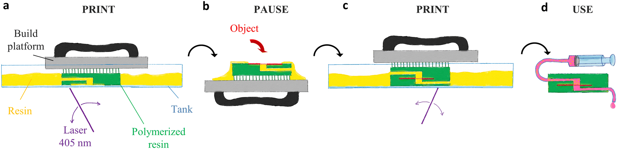 | ||
| Fig. 1 Concept illustration of the print-pause-print strategy. a) Printing of a first part (pre-pause part). b) Pausing, removal of the building platform, removal of resin excess and positioning of the object to integrate. c) Resuming of the print (post-pause part). d) Cleaning and developing of the detached chip. | ||
3. Pause the print after the slot is printed.
4. Remove the platform from the printer and remove the excess of resin on top of the pre-pause part.
5. Place the object in the slot – or for thin object, on top of the pre-pause part (Fig. 1b).
6. Put the platform back on the printer. A remaining thin film of resin helps the adhesion of the object below the print by capillarity.
7. Resume the print (Fig. 1c).
8. Repeat the steps 3–7 for integrating several objects.
9. At the end of the print, detach the chip from the platform, remove the support pillars, clean and develop the chip and channels with solvents.
10. UV post-curing and use of the chip (Fig. 1d).
In particular, we incorporated planar and non-planar objects made of a variety of materials, including semipermeable polymeric porous membranes, elastic membranes, glass coverslips, microfabricated silicon filters, paper pads, sacrificial films, steel balls and silicone O-rings. We demonstrated improved functionalities from basic flow control (Quake's valve and fluidic check valve), optical windows for high-resolution imaging (fluorescent imaging of bacteria), fabrication of shallow channels, integration of dried solutions, and inflow capture and culture of mammalian cells. Far from demonstrating all the possibilities offered by PPP, this report presents a new toolbox for upgrading SLA-based chips built from commercial printers.
Material and methods
Printing
Designs were drawn on Fusion 360 (Autodesk) and converted into .stl files, available as ESI.† Cross section of the chips are also available in Fig. S1 and S2.† These files were then sliced using proprietary softwares Nauta and Fictor (DWS Systems) or Pre-form (Formlabs) and printed with a 700 μm base and 2.3 mm high, 700 μm wide support pillars using a DWS 029J+ printer (DWS Systems) with a transparent and biocompatible resin (DS3000, DWS Systems). The integration of a semipermeable membrane was carried out on a Form 3B+ printer (Formlabs) with a Clear (v4.0) resin (Formlabs). Printing parameters are listed in the Table S1.† Completed prints were detached from the platform, support pillars were cut, and the print was developed using isopropanol or acetone (CMC materials), while the channels were additionally flushed with syringes and ultrasound cleaning (5 min, 37 kHz, 150 W, Elmasonic S 100H, FisherBrand) (Fig. 1d). Printed chips were then post-cured during 15 min at 405 nm, 5.5 mW cm−2 (FormCure, Formlabs). For mammalian cell culture chips, a post-bake step was performed during 2 h at 120 °C in an oven. For the integration of coverslips after the printing of channels, an extra-illumination without resin in the tank was required (see Fig. S3†).Coverslip preparation
Glass coverslips (thickness 140 ± 20 μm, diameter 10 or 18 mm, Immuno-Cell) were silanized to increase resin-glass adhesion. Coverslips were cleaned with acetone and isopropanol and plasma treated during 5 min (air plasma, 50 W, 0.5 mbar, Pico, Diener Electronic). They were then immersed in a solution of ethanol (Micropur), 0.01% v/v of glacial acetic acid (Sigma-Aldrich) and 2% of (3-aminopropyl)trimethoxysilane (MAPTMS, Sigma-Aldrich) during 1 h. They were finally cleaned with ethanol, dried with nitrogen and stored before use.X-ray tomography
X-ray tomography was performed on an EasyTom XL 150 (RX Solutions) containing a 1920 × 1536 pixels flat panel sensor and a sealed source (Micro 150, RX Solutions). Chips were scanned in rotation (1440 projections, angle steps of 0.25°). The source currents and a tube voltages used are listed in Table S2.† Acquisition was performed at 10 frames per second and averaging 5 images per projection. Cross-section images with pixel size between 4.0 μm and 11.9 μm were obtained after treatment with the XAct software, including, brightness/contrast modifications and noise filtering (RX Solutions). On the cross-section figures, all the chips are presented with the first printed layer facing upward and the last layer downward.Xurography of water-soluble films
Water-soluble films (20 μm thick, vinyl acetate, Au fil d'Emma) were cut using a cutting plotter (FC8600-60, Graphtec) and the following parameters: blade CB09U (900 μm in diameter), blade thickness 150 μm, force 22 A.U., speed 10 cm s−1.Scanning electron microscopy
Electronic microscopy was performed with a S-3700 microscope (Hitachi) for the sacrificial channel micrographs (voltage 1 kV, current 33 μA), 30 measurements were carried on each sample and repeated over 3 samples. Silicon filters were characterised using an i600 microscope (HELIOS NanoLab, FEG Schottky, current 43 pA, voltage 30 kV).PDMS membrane preparation
The PDMS membranes for the valves were framed by a specialized double-sided tape (5302A-50, Misumi) composed of a PET film, a silicone adhesive, an acrylic adhesive and their liners. The tape was first cut by xurography (same parameters as for the water soluble films) in 6 mm circles with an 1.5 mm empty square in the middle. Sylgard 184 PDMS was spin-coated (2000 rpm, 60 s, resulting thickness 23 μm) on the backside of a polystyrene Petri-dish and cured during 3 h at 60 °C. A first tape was bonded to the PDMS membrane (silicone adhesive side). The PDMS membrane was cut around the tape, removed from the Petri surface, and a second tape was bonded to the other side of the PDMS membrane. Before integration, the last liners on the acrylic adhesive sides were removed.Pressure and valve tests
Pressure resistance tests for the integration of coverslips were carried out by applying pressure through a silicone tubing (3 mm OD, 1 mm ID) containing DI water and connected to the central channel of the chips using a pressure regulator connected to the building pressurised air (10 bars maximum). The outlet of the central channel was connected to a closed tubing. Pressure was manually increased until a leakage appeared or the tubing detached from the connectors (around 4 bars).Valve pressure tests were carried using a MFCS-EZ pressure controller (Fluigent SA) connected to a pressurised nitrogen source (1200 mbars). Pressure was applied on a DI water reservoir linked to the microfluidic chips using silicone tubing (3 mm OD, 1 mm ID). Flow rate was measured using a L+ Flow Unit (Fluigent SA) flowmeter at the outlet of the chips. For the valve test, constant pressure was applied on the flow channel (75 mbars), while the air pressure within the control channel was switched between 0 and 200 mbars every 20 seconds while monitoring the induced flow rate in the flow channel (3 cycles per chips). For the check valve, a ramp of pressure difference (pressure at the open direction inlet minus the difference at the close direction inlet) from 100 mbars to −300 mbars, then from −300 mbars to 100 mbars was applied three times to three different chips using two pressure sources while monitoring the flow rate in the open direction.
Bacteria culture and imaging
Bacteria used for imaging were the wild-type clinical Escherichia coli strain SP15 transformed with the plasmid pFPV25.1, containing a carbenicillin resistance cassette and the GFP (green fluorescent protein) gene controlled by a constitutive promoter.28 Bacteria were grown overnight at 37 °C in LB broth (Lennox, Invitrogen) with the carbenicillin antibiotic (50 μg mL−1) at 200 rpm agitation. The culture was then diluted 1/10 in LB carbenicillin (50 μg mL−1) and incubated at 37 °C with 180 rpm agitation to reach the exponential phase (optical density at 600 nm, 0.5). The chip was then inoculated and closed for imaging.Live imaging was achieved with an inverted microscope Ti2 Eclipse (Nikon), a camera (Pco.edge 4.2 bi) and a light source (Sola, Lumencor). Bacteria were imaged using differential interference contrast (DIC) and GFP fluorescence with a specific filter (GFP-3035D, Nikon) and a 40× objective (MRD00405, Nikon). For the tracking of E. coli, bacteria were imaged for 4 hours every 10 minutes at 37 °C at different positions in the chip.
Images were processed and analysed using Fiji and Ilastik for segmentation and bacteria counting.
Integration and test of nanoporous membranes
Two types of nanoporous membranes were tested: commercial cation-selective membranes of Nafion 115 (dry thickness 100 μm, provided by Ion Power), and non-selective PET (poly(ethylene terephthalate) membranes (Good Fellow film ref. ES301130), track-etched by swift heavy ion irradiation (Kr 7 Mev/nucleon) at GANIL (Grand Accélérateur National d'Ions Lourds, Caen).29 The PET membrane had pore density of 108 pores per cm2, pore diameter of 190 nm, and thickness of 13 μm. Membranes were clamped between 3D-printed supports using screws or included using the PPP protocol. In both cases (clamped, or PPP) these membrane supports were then assembled with two other 3D-printed pieces which contain the electrodes and the liquid inlets and outlets. The two same auxiliary pieces and electrodes were used for all the experiments reported here. For PET membranes, the printing-layer thickness was 25 μm and the membrane slot was 1-layer thick, while for Nafion membranes, the printing-layer thickness was 50 μm and the membrane slot was 2-layer thick. Membrane supports and the two other pieces of the electro-chemical cell were printed using a Formlab Form 3B+ printer, with a “Clear v4” resin. Printed elements were rinsed 1 h in isopropanol, and then soaked in KCl solutions overnight (at the same concentration as the experiments). Open circuit voltage and electrical resistance of the membranes were measured by placing the membrane between two potassium chloride (KCl) electrolytes of respective concentration c1 and c2, with silver chloride (AgCl) electrodes as working and counter electrodes. The surface of the membrane in contact with the electrolytes was 5 mm2. For Nafion membrane, concentration used were c1 = 1.3 × 10⁻² mol L−1 and c2 = 1.3 mol L−1. For PET membranes, c1 = c2 = 1.35 × 10⁻¹ mol L−1 or 1.35 × 10⁻² mol L−1.Silicon-based filters: design and fabrication
The cleanroom fabricated silicon filters presented in Fig. 8a and b exhibited a circular filtering membrane of 1 mm diameter and 1.4 μm thickness with 2130 pores of 10 μm diameter each. The membrane was surrounded by 200 μm wide non-filtering fluidic slits. The membrane was composed of a SiO2/Si3N4 bilayer (800 nm and 400 nm respectively). Electrodes of 150 nm (50 nm Cr/100 nm Au) were indexing 6 pores of the filtering membrane for electrical sensing and analysis of captured elements and were insulated with a 1 μm layer of Si3N4. Finally, the squared shape silicon supporting structure of 1 cm sides and 250 μm thickness conferred rigidity to the device and allowed handling while protecting the thin filtering membrane.The microfabrication process included five lithography steps. Chemical vapour deposition (CVD) and physical vapour deposition (PVD) techniques were used to deposit respectively ceramic and metal layers on the wafer, which were then patterned through plasma reactive ion etching (RIE). The first mask level (L1) corresponded to the electrolytic growth of the electrical contact pads on the front face of the devices. The microelectrodes, connection tracks and electrical contact pads were defined on the same second level (L2). The insulation of the connection tracks and contact pads was defined on the third level (L3). A fourth level (L4) corresponded to the opening of the pores of the filtering membrane and the lateral fluidic slits. Finally, a fifth and last level (L5) formed the supporting structure through the backside plasma etching of the silicon substrate. Detailed fabrication protocol is present on (ESI† document 1).
Cell culture and capture
Cells used for the capture experiments were obtained from the culture and amplification of prostatic cancer cell line (PC3) with a genetic modification for the expression of a cytoplasmic green fluorescent protein (GFP) and the resistance to the geneticin antibiotic (G418) as to keep a selection pressure during cell culture. Culture media consisted in RPMI 1640 (Gibco) with 10% of fetal bovine serum and 1% penicillin (Gibco) and G418 (Gibco). Cells were passed once 70–80% confluence was reached in T25 culture flasks within 5 mL of culture media. Before experiments, cells were transferred in 5 mL of PBS at a concentration of 1000 cells per mL.Live video of the cell capture was obtained with an inverted Olympus microscope (IX73), a camera (Hamamatsu Orca Flash 4) and an epifluorescent light source (Lumencor Sola 6) covering the needed excitation for GFP fluorophores. Cell solution was pushed with a CETONI Base 120 syringe pump within 1.6 mm tubing (Fluigent SA).
During the pre-processing step, 10 mL of ethanol was flushed through the tubing and the 3D printed chip to obtain a good wettability and avoid bubble formation, followed by a cleaning with 20 mL of PBS, and finally 4 h incubation with 1 mg mL−1 of fibronectin. Cell sample was then pushed at 1 mL min−1. At the end of the capture, cell media was pushed in the chip, which was then placed in an incubator (37 °C, 5% CO2) for three days. Bright field images of cultured cells were obtained with an inverted microscope (AE31, Motic).
Results and discussions
Alignment during PPP
Before integrating objects, we checked on our DWS 29J+ printer that the repositioning of the platform after removing it from the printer did not lead to significant misalignment of post-pause layers compared to the pre-pause part. For that, an alignment structure was printed, with an inner cross in the pre-pause part, and an outer cross in the post-pause part (Fig. 2a and b). The angle α and shifts in the plane between the inner and outer crosses, or respectively the pre-pause and post-pause layers, were measured for 3 runs, 4 samples per run (angle in red, positions in yellow and blue in Fig. 2b). A control structure was built on the same run, with no pause between the inner and outer cross, to test the precision of the measurement (Fig. 2b, right). No significant misalignment was visible between the test structure with PPP and the control structure (mean x-shift −12.9 ± 24.8 μm vs. 6.6 ± 16.1 μm; y-shift 20.6 ± 32.4 μm vs. 3.5 ± 26.2 μm; α angle −0.1 ± 0.3° vs. 0.0 ± 0.4°), with a maximum shift of 90.4 μm. With no significant misalignment, we first tested the integration of a simple planar object: a glass coverslip. | ||
| Fig. 2 Precision of the realignment during the PPP process. a) Picture of an alignment structure. b) Schematic of the measurement with an exaggerated misalignment (left) and a control structure (right): α angle between the inner and outer cross; position of the centre of mass of the inner cross (yellow) and outer cross (blue). c) Angle and shift between the inner and outer crosses, measured with 12 samples per conditions, 4 samples per print. Error bars represent ± one standard deviation. | ||
Imaging windows and shallow chambers
Several features of the SLA drastically limit the optical imaging inside 3D-printed chips, including the auto-fluorescence of most transparent resins, their inhomogeneity and the roughness of the surfaces. Although the outer surfaces of the chip could be treated to make them smoother,30 high-resolution imaging inside 3D-printed chips has still not been reported, to the best of our knowledge. Herein, we integrated circular coverslips with thicknesses of 140 μm to create imaging windows. Methacrylated coverslips were integrated in a 150 μm-thick slot before the printing of 1 mm-high, 2 mm-wide channels separated by walls of 1 mm, 500 μm or 200 μm width (see tomography image in Fig. 3a). Pressure tests were performed for each wall thicknesses on 3 samples to characterise the maximum pressure withstood in the central channel before leakage. The chips with 1 mm-wide walls leaked at 2, 3.6 and 2.5 bars. The chips with 500 μm-wide walls withstood up to 4 bars. One chip with 200 μm-wide walls broke at 3.2 bars, the other ones held up to 4 bars. With the lowest failure pressure at 2 bars, such integration has been proven as being robust and compatible with typical pressure range used in microfluidic applications. Such high resistance was due to the surface treatment of the coverslips, adding methacrylate moieties that covalently bonded with the resin under UV illumination. | ||
| Fig. 3 Imaging windows and shallow chambers. a) Tomographic cross section of the integration of a coverslip before printing the channels. b) Cross section of the integration of a coverslip after printing the channels, with a zoom-in in insert. c) Cross section of the double coverslip chip, with a thin channel between the two coverslips. In insert, vertical grey values profile (averaged over 1700 μm). d) DIC and GFP imaging of SP15 pFVP25.1 E. coli. bacteria inside the glass–resin chip (illustrated in b) and the glass–glass chip (illustrated in c). e) Histogram of the fluorescent background noise for the glass–resin chip (grey) and the glass–glass chip (black). Higher grey values correspond to higher light intensities. f) Growth curves of bacteria imaged on the coverslip surface in the glass–glass chip, for 5 different locations in the imaging windows. Error bars are standard deviations. | ||
Integration of a coverslip was also possible after the printing of the channels. In this case, an extra step is required to bond the coverslip to the pre-pause layers (Fig. S3†). By closing a pre-existing channel, shallower channels were created compared to monolithic channels, limited to 150 μm in height with our printer due to over-penetration of the light inside the channel (Fig. S4†). Here, we created 100 μm-thick channels, over a large area of 9 mm × 6 mm supported by two 4 mm-long, 500 μm-wide pillars (see tomography image on Fig. 3b). As a proof of concept, we tested imaging of an Escherichia coli expressing green fluorescent protein (GFP) through this coverslip (Fig. 3d). DIC and fluorescence images were obtained, but a large background noise due to the resin thickness impeded the tracking and efficient counting of bacteria.
In order to improve imaging capabilities, we created a double imaging window by sandwiching a thin channel between two coverslips (10 and 18 mm in diameter) as seen on Fig. 3c. The final channel height has been measured to approximately 28 μm, without any leakage even at the high pressure applied with a syringe during the resin flushing. With this design, we imaged E. coli using DIC and fluorescence modes (Fig. 3d), showcasing to the best of our knowledge the first tracking of 1 μm wide micro-organisms in a 3D printed chip (Movies S1 and S2†). Moreover, this chip enabled to image bacteria at several locations in real time for 4 hours with a lower background noise as regard to the chip with the resin above the chamber (Fig. 3e). Segmentation, which is often critical and requires high image resolution, was carried out on 5 locations along the 4-hour imaging. Bacterial counting of E. coli in the focal plane indicated bacterial division until 80 minutes of on-chip culture followed by a stationary phase until the end of the experiment, which is in line with E. coli different phases of growth (Fig. 3f).
Shallow channels with sacrificial films
As shown above, creating shallow (e.g. <2 layers height ≈100 μm) channels is a challenge with SLA printers, especially commercial ones. Several groups proposed hardware modifications to create shallow channels. For example Xu et al. designed a secondary build platform covered with PDMS (reaching channel height down to 10 μm).31 Boaks et al. developed a custom resin, absorbers and filters for UV light (minimum channel height 20 μm).32 Parameters have been finely tuned (exposure and slicing) to limit the UV over-exposure.1 Herein, we propose the integration of sacrificial films which are not soluble in contact with both the SLA resin and isopropanol for the creation of monolithic shallow channels with commercial printers. 20 μm-thick water-soluble films were cut by xurography into 5 mm-wide squares, either plain (Fig. 4a left), or containing 800 μm wide holes (Fig. 4a centre) or 2 mm-long and 1 mm, 500 μm, 300 μm or 200 μm-wide structures (Fig. 4a right). These films were incorporated in between two open reservoirs. After development and post-curing, the chips were immersed in 40 °C water during 2 h with ultrasound and 72 h at RT water. The solubilised film was replaced by red dye (E110 food dye, Les Artistes). As seen in Fig. 4b, the films have been fully solubilised, creating channels with width down to 200 μm. The shallow channel was imaged by SEM after breaking in half three plain chips and measured along the channel in 30 positions as 22.7 ± 0.7 μm (mean + standard deviation), 24.0 ± 1.4 μm and 20.3 ± 1.3 μm, showing a constant thickness over 5 mm and smooth surfaces.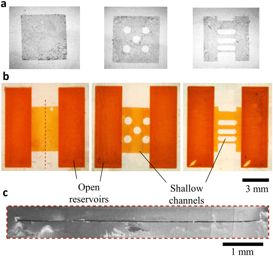 | ||
| Fig. 4 Shallow channels with sacrificial films. a) Pictures of the xurographed soluble films before integration. b) Pictures of red dye in the chips after film integration and solubilisation. c) SEM image of the chip in b-left, cut in half following the red line on b. | ||
Reagent storage
For analytical applications, it is often required to trap and store dry reagents inside a closed chip.33 Here, we are presenting two different strategies, using colour dyes as samples for two proofs of concept.In a first example, reagents were loaded in linter cotton paper pads after their incorporation and printing, dried then re-suspended. The 2 mm-wide, 700 μm thick pads were cut using a biopsy puncher from a sheet of blotting paper (330 g cm−2, BF3 grade, Sartorius Stedim Biotech). Three paper pads were integrated inside a large chamber (see Fig. 5a). After development and cleaning, 5 μl of food dyes (orange: E110; green: E102, E124 and E131; purple: E124 and E151, Les Artistes) was deposited on top of the paper pads by a small access port on top of each pad. The dyes were then absorbed by the pads and let to dry, proving that the paper porosity was still present after its immersion in the resin and development. After the addition of DI water in the channel, the dyes slowly diffused out of the pads, as seen on the Fig. 5b and Movie S3,† showing the successful release of reagents.
 | ||
| Fig. 5 Reagent storage. a) Tomographic cross section of the chip with paper pads after ink loading. b) Time-lapse of the ink diffusion after water addition in the channel. c) Time lapse of the film solubilisation and ink diffusion after water addition in the channel. | ||
In a second example, 8 μl of blue dye (E131) was pipetted on top of well-cleaned pre-pause layers during the pause and let drying. On top of the dried dye spot, a 25 μm-thick water-soluble film (Avalon Film, Madeira) was added in order to protect it during the subsequent printing steps. The dye spot was therefore not in contact with the resin and the isopropanol used during the development. After the addition of DI water in the channel, the film slowly solubilised and the dye spot diffused inside the water (Fig. 5c and Movie S4†), demonstrating a second method for reagent storage and resuspension inside 3D printed chips. Here, diffusion was slower compared to the first example, due to the solubilisation time of the film.
Valves and fluid control
Flow control is primordial in microfluidic systems, and active/passive components to stop, divert or regulate flows are building blocks for advanced microfluidic networks. The best-known examples are “Quake” valves, where a pressurised actuation channel pushes an elastic PDMS membrane inside a fluidic channel in order to reduce its section or to completely obstruct it.6 Such valves have then been adapted to create reconfigurable microfluidic networks,34–36 peristaltic pumps,37 pressure regulators…38 Here, we propose to integrate inside a 3D-printed chip an elastic membrane to create such a valve. Due to their oxygen permeability, silicone and PDMS membrane inhibited the curing of resin at its vicinity and impeded the bonding of the membrane to the pre and post-pause layers. We therefore chose to mask the PDMS membrane on both side with double-sided tape frames (see Fig. 6a). The tape is composed of a silicone adhesive and an acrylic adhesive. For this integration, the pre-pause layers were cleaned using isopropanol to insure a direct bonding of the acrylic adhesive on these layers. For three different chips, actuation pressure was switched from 0 to 200 mbar for 20 seconds, and the flow monitored in the fluidic channel (see Fig. 6b). For all the chips, the flow immediately stopped when the pressure was applied in the actuation channel. When the pressure was released, the flow rate went back to the previous value, with a maximum difference of 75 μL min−1 (8%) between two valves (n = 3). Despite an imperfect bonding between the tape frames and the pre-pause layers, all the valves successfully blocked the flow, opening the routes to more complex fluidic operations in 3D printed chips. | ||
| Fig. 6 Valves and fluidic diodes. a) Tomographic cross section of the valve chip containing a PDMS elastic membrane masked with tape frames. b) Temporal variation of the flow rates for 3 different chips during actuation pressure pulses. c) Tomographic cross section of a check valve. d) Flow rate in the open direction depending on the pressure difference, for three pressure ramps in both directions, for 3 diode chips. | ||
Passive valves are also part of the classical fluidic toolbox, especially check valves (or diodes) that allow the flow only in an open direction, and block the flow from a close direction.39–41 Here, we propose to reproduce a design from Morgan et al. where a stainless steel ball can be pushed against a silicone O-ring to block the flow (close direction), or sent in a larger channel by a flow in the opposite, open direction (see Fig. 6c).42 During fabrication, a steel ball (1 mm diameter, 1598K16, Mc Master-Carr) was first inserted in the vertical channel during the pause, then a O-ring (fluoroelastomer, 1284N101, Mc Master-Carr) was placed in the dedicated slot, and the printing resumed. Although neither object is planar, integration succeeded for the three fabricated diodes. For the three diodes, on the open direction, the flow rate quickly increased with the pressure after an initial threshold (up to 50 mbars see Fig. 6d), for a flow rate around 800 μL min−1 at 100 mbar approximately. In the close direction, the flow rate started to increase, with a maximum at 68 μL min−1, until the flow pushed the ball against the O-ring, decreasing the flow rate as the pressure continued to rise. For both directions, hysteresis is present due to the different ball positions at the beginning of the pressure increase and decrease. Overall, all diodes presented a large difference of flow behaviour between the open and close direction.
Nanoporous membranes
Nanoporous membranes are regularly used inside microfluidic chips for applications like particle filtering, blue electricity generation and organ-on-chips. Here, we aimed to demonstrate that the integration of nanoporous membranes with the PPP process preserve the performance (resistance and selectivity) of such membranes, with an electrical characterisation usually performed for blue energy testing.43 Here, electrical resistance of non-selective PET membranes and semipermeable, cation selective Nafion membranes were studied in an electrochemical cell, for membrane clamped between two 3D-printed support and membranes included in these supports by PPP (Fig. 7a). Results are presented in Fig. 7b–d: the imposed electric current through the membrane (I) is plotted versus the resulting potential difference between the silver-chloride electrodes (U). The resistance of the cell (including the membrane) is the inverse of the slope. For non-selective PET membranes, the current (hence the total resistance of the cell) measured with PPP membranes was very close to the current measured for clamped membranes (Fig. 7b and c). The results are slightly more scattered when the membranes were integrated by PPP than when they were clamped, especially at low concentration. Overall, PPP integration of nanoporous PET membrane was successfully achieved. | ||
| Fig. 7 Nanoporous membranes. a): Configuration of the 3D printed electro-chemical cell for membrane characterisation. The mounted membrane (1) separates two electrolyte reservoirs of concentration c1 and c2. The electrical circuit is closed by silver-chloride electrodes (2) allowing a current I to flow and to measure the voltage across the cell. Electrical characterization of b and c) nanoporous PET (non-selective) at two different concentrations and d) Nafion membranes in a salt gradient (cation selective). n = 3 for clamped membranes and n = 4 for PPP membranes. | ||
Nafion membranes are selective and hence, they were tested in a gradient of concentration (ratio = c2/c1 = 100). The open-circuit voltage (OCV) was the same for clamped or for PPP-inserted membranes (Fig. 7d), meaning that the selectivity was not affected by the process (same OCV). However, the total resistance of the chip was slightly higher for PPP-inserted membranes, which we hypothesize by the clogging of some pores by the resin. The Nafion membrane therefore still presents the expected properties of ion-selective membranes: good selectivity and low resistance.
As a consequence, nanoporous membranes of Nafion and PET can be inserted in electro-chemical cells using the PPP protocol without clogging the membrane nanopores, hence preserving their functionality (resistance, and selectivity).
Microfabricated filters
Finally, in our last example, we integrated more complex objects inside microfluidic chips: silicon-based microfilters, fabricated in clean room using standard lithography and etching techniques. These porous membranes were initially developed for partial cell capture within complex fluids such as whole blood (Fig. 8a and b). Pores of 10 μm were obtained with high accuracy by lithography and etching, for cell trapping based on their size and deformability. Open fluidic slits allowed a partial filtration of the sample: the flow is distributed through both the surrounding slits and the microperforated membrane, releasing the pressure of the filtering membrane and therefore achieving larger flow rate for sample processing while reducing mechanical stress on captured elements. Sensing electrodes were integrated on the membrane for electrical analysis of the collected sample. Characterization of the electrodes is shown in ESI† document 2, proving that they were electrically accessible; however, significant optimization of the electrode is required for the electrical sensing of captured cells. This aspect is still under development and will not be addressed here.44 | ||
| Fig. 8 Microfabricated filters. a) Pictures of microfabricated filters exhibiting the porous circular membrane in the centre and 12 electrical contact pads. b) SEM micrograph of the porous circular membrane supporting sensing electrodes and surrounded by fluidic slits formed by the silicon supporting structure. c) Tomographic cross section showing the subsequent integration of a glass coverslip and a microfabricated filter within a 3D printed fluidic channel. d) Pictures of the 3D printed chip. e) Fluorescence microscopy during the capture of PC3 GFP cells in PBS. f) Bright field image of trapped cells on the membrane at day 0 and day 2, after media renewal. | ||
The microfabricated filter was integrated inside a 3D-printed microfluidic chip to create a crossflow capture arrangement, and to facilitate the imaging during the cell capture and culture, thanks to a co-integration with a coverslip (Fig. 8c, e and f). The chip dimensions matched the one of a small Petri dish, fitting in an inverted optical microscope with the fluidic connectors to a syringe pump placed on top of the chip. Capture of GFP-fluorescent PC3 cells (immortalised cell line from a bone metastasis of a prostate adenocarcinoma) was realised in a PBS solution at a flow rate of 1 mL min−1. Capture was rather homogeneous on the membrane, as seen on Fig. 8d. The real-time imaging along the experimental is available as a video in the ESI† (Movie S5). In the future, the correlation between the fluorescence signal and the electrical impedance sensing of cells in between the electrodes may provide in situ and synchronous detection of capture events.
Finally, we demonstrated the culture of trapped cells directly on the membrane, proving the cyto-compatibility of this integrated 3D-printed chip. After trapping, the cells were cultured with medium for three days, and imaged through the coverslip with bright field microscopy (Fig. 8f after trapping and after 3 days and a medium renewal). The PC3 cells displayed their characteristic fibroblast-like shape, which confirmed both their viability and adhesion to the substrate. Such proof-of-concept opens the doors for long-term culture of collected samples and in situ, electrical and optical biological analysis.
Limitations/discussions
This new concept of integration has been demonstrated through the incorporation of various objects and added functionalities. Its implementation did not require extensive optimisation and proved to be robust, with a high successful fabrication rate of chips. This strategy is also reliable from sample to sample, as seen with the triplicate experiments for the imaging windows valves, diodes, sacrificial films, semi-permeable membranes, as well as the reagent storage experiments (data not shown). It should be noted that our printer was located outside a clean room, without special care to avoid dusts or particles. However, we wish to draw the attention on some key points and limitations, for those who would like to contribute to this new toolbox:• Pausing and resuming prints are not available in all SLA printers, even if it is a feature more and more present on commercial printers. We tested such feature on the 029J+ (DWS Systems) and form 3 (Formlabs) printers, even if most of the work present here has been done with the first one.
• Realignment between the pre-pause and post-pause layers has been checked only with the 029J+ printer and depends on how the print platform is attached and secured. Results may differ with other printers. We did not test the alignment between the object to integrate and the pre-pause layers. However, for objects thicker than a print layer, the manual alignment was facilitated by a slot corresponding to the object shape (with 500 μm margins) in the pre-pause part.
• Only two transparent resins were presented here. Integration of coverslips, especially with large overhangs (as presented in Fig. 3a) could not be completed without breaking the coverslip while using a more viscous resin (DL260, DWS Systems). The integrated object experienced large forces when the print re-entered the resin vat and displaced the resin below it. A large suction force was also present when the printer's platform moved up after finishing a layer.
• In this study, the only object for which the adhesion to resin has to be improved were coverslips, using treatments with methacrylated silanes. PMDS could not be incorporated, even if silanized and vacuumed before integration: its high oxygen permeability and sorption inhibited the curing of resin at their vicinity.
• For opaque objects such as the microfabricated filter, bonding to the pre-pause layers were not perfect and limited delamination was visible (Fig. 6a and 8c) without an impact on the performance of the functionalities. Indeed, the printer laser did not reach the resin trapped between the pre-pause layers and the object, and part of it was removed during development. The remaining resin was nevertheless polymerised during the UV post-curing steps, reinforcing the object/pre-pause layers bonding.
• We sometimes observed higher deformation of the microfluidic chips, probably due to shrinkage, which are able to deform integrated coverslips (see Fig. 5a or 6a). While such shrinkage depends on the geometry of the design, we did not observe it reproducibly between batches and did not investigate it further.
Conclusions
In this study, we demonstrated the use of an integration method, called “print-pause-print”, for 3D-printed microfluidic chips. With this strategy, we showed that we can overcome one of the limitations of SLA-based microfluidics, purely monolithic chips, and fabricate hybrid devices containing several materials (resin, glass, silicon, paper, plastic…), thus opening the ways towards a toolbox of new functionalities in 3D-printed chips. Here, we showed several examples of such functionalities, including valves, high-resolution imaging, creation of shallow channels, reagent storage, incorporation of semipermeable membrane and microfabricated filters used for cell trapping and culture. To the best of our knowledge, this PPP strategy showed for the first time imaging and tracking of individual bacteria in 3D-printed chips. The integration of cleanroom fabricated devices further demonstrated the ability of SLA 3D printing to fill the current gap in cleanroom packaging of small devices for microfluidic applications. No leakage has been observed at working pressures for all the showed examples, proving the robustness of this integration method, especially with complex channel networks around the object to incorporate.As a perspective, we aim at expanding the fluid control toolbox with other membrane-based units (peristaltic pumping, pressure regulator, normally closed or open valves) as well as to reduce the size of these units.
Author contributions
M. S.: investigation, methodology, writing for the microfabricated filter section. T. D.: investigation, data curation for the nanoporous membrane section. P. G.: investigation, data curation, methodology and writing for the bacteria imaging section. Y. D.: supervision, funding acquisition, writing – review and editing for the bacteria imaging section. J.-P. N.: supervision, funding acquisition, writing – review and editing for the bacteria imaging section. C. T.: supervision, methodology, funding acquisition, writing for the nanoporous membrane section. V. R.: conceptualisation and methodology for the valve and sacrificial channel sections. L. M.: investigation (X-ray tomography), methodology, funding acquisition. B. V.: investigation, conceptualisation, funding acquisition, methodology, supervision and writing.Conflicts of interest
All authors declare that they have no conflicts of interest.Acknowledgements
The authors would like to acknowledge Marie-Charline Blatché (LAAS-CNRS, Toulouse, France) for her support in cell culture experiments, Julie Foncy (LAAS-CNRS, Toulouse, France) for her support in 3D printing, Paul Duru (IMFT, Toulouse, France) for the X-ray tomography, David Bourier and Aurélie Lecestre (LAAS-CNRS, Toulouse) for clean-room process development, Mathilde Lepoitevin (IMAP, Paris, France) for providing the PET nanoporous membranes, Christophe Vieu, Hervé Aubert (LAAS-CNRS, Toulouse, France) and Aline Cerf (Smartcatch, Toulouse, France) for their scientific advising. This work was supported by the French RENATECH network, the MultiFAB project funded by FEDER European Regional Funds and French Région Occitanie (16007407/MP0011594), by the HoliFAB project funded by the European Union's H2020 program (760927) and by Nanofutur project, funded by the ANR (21-ESRE-0012). P. G. was supported by a grant from the region Occitanie Midi Pyrénées and the University of Toulouse (ADI program), and by the grant EUR CARe (ANR-18-EURE-0003) in the framework of the Programme des Investissements d'Avenir. Y. D. was funded by the European Research Council (ERC) under the European Union's Horizon 2020 research and innovation programme (grant agreement no 803074).References
- J. L. Sanchez Noriega, N. A. Chartrand, J. C. Valdoz, C. G. Cribbs, D. A. Jacobs, D. Poulson, M. S. Viglione, A. T. Woolley, P. M. Van Ry, K. A. Christensen and G. P. Nordin, Nat. Commun., 2021, 12, 5509 CrossRef CAS PubMed.
- A. Accardo, R. Courson, R. Riesco, V. Raimbault and L. Malaquin, Addit. Manuf., 2018, 22, 440–446 CAS.
- L. A. Pradela Filho, T. R. L. C. Paixão, G. P. Nordin and A. T. Woolley, Anal. Bioanal. Chem., 2024, 416, 2031–2037 CrossRef CAS PubMed.
- L. A. Milton, M. S. Viglione, L. J. Ye Ong, G. P. Nordin and Y.-C. Toh, Lab Chip, 2023, 23, 3537–3560 RSC.
- A. Amini, R. M. Guijt, T. Themelis, J. De Vos and S. Eeltink, J. Chromatogr. A, 2023, 1692, 463842 CrossRef CAS PubMed.
- M. A. Unger, H. P. Chou, T. Thorsen, A. Scherer and S. R. Quake, Science, 2000, 288, 113–116 CrossRef CAS PubMed.
- M. P. Wolf, G. B. Salieb-Beugelaar and P. Hunziker, Prog. Polym. Sci., 2018, 83, 97–134 CrossRef CAS.
- R. F. Ismagilov, J. M. K. Ng, P. J. A. Kenis and G. M. Whitesides, Anal. Chem., 2001, 73, 5207–5213 CrossRef CAS PubMed.
- M. L. Chabinyc, D. T. Chiu, J. C. McDonald, A. D. Stroock, J. F. Christian, A. M. Karger and G. M. Whitesides, Anal. Chem., 2001, 73, 4491–4498 CrossRef CAS PubMed.
- K. J. Lee, K. A. Fosser and R. G. Nuzzo, Adv. Funct. Mater., 2005, 15, 557–566 CrossRef CAS.
- R. Fu, B. Xu and D. Li, Int. J. Therm. Sci., 2006, 45, 841–847 CrossRef.
- V. Saggiomo and A. H. Velders, Adv. Sci., 2015, 2, 1500125 CrossRef PubMed.
- D. Chen and X. Zheng, Sci. Rep., 2018, 8, 9139 CrossRef PubMed.
- V. Fournié, B. Venzac, E. Trevisiol, J. Foncy, J. Roul, S. Assie-Souleille, M. Escudero, P. Joseph, A. Reitz and L. Malaquin, Addit. Manuf., 2023, 72, 103629 Search PubMed.
- D. Han, C. Yang, N. X. Fang and H. Lee, Addit. Manuf., 2019, 27, 606–615 CAS.
- G. Lipkowitz, T. Samuelsen, K. Hsiao, B. Lee, M. T. Dulay, I. Coates, H. Lin, W. Pan, G. Toth, L. Tate, E. S. G. Shaqfeh and J. M. DeSimone, Sci. Adv., 2022, 8, eabq3917 CrossRef CAS PubMed.
- D. P. de Jesus and J. A. F. da Silva, Lab Chip, 2023, 23, 3694–3703 RSC.
- Y. T. Kim, A. Ahmadianyazdi and A. Folch, Nat. Protoc., 2023, 1–17 Search PubMed.
- Q. Song, A. Hamza, C. Li, A. S. Sedeky, Y. Chen, M. Zhu, A. Goralczyk, F. Mayoussi, P. Zhu, P. Hou, C. Piesold, D. Helmer, B. E. Rapp and F. Kotz-Helmer, Addit. Manuf., 2024, 81, 103991 CAS.
- A. Lace, A. Byrne, S. Bluett, L. Malaquin, V. Raimbault, R. Courson, Z. Hayat, B. Moore and E. Murray, J. Sep. Sci., 2022, 45, 1042–1050 CrossRef CAS PubMed.
- F. Li, N. P. Macdonald, R. M. Guijt and M. C. Breadmore, Lab Chip, 2019, 19, 35–49 RSC.
- C. W. Pinger, A. A. Heller and D. M. Spence, Anal. Chem., 2017, 89, 7302–7306 CrossRef CAS PubMed.
- P. K. Yuen, Biomicrofluidics, 2016, 10, 044104 CrossRef PubMed.
- G. Scotti, S. M. E. Nilsson, M. Haapala, P. Pöhö, G. B. af Gennäs, J. Yli-Kauhaluoma and T. Kotiaho, React. Chem. Eng., 2017, 2, 299–303 RSC.
- M. Banna, K. Bera, R. Sochol, L. Lin, H. Najjaran, R. Sadiq and M. Hoorfar, Sensors, 2017, 17, 1336 CrossRef PubMed.
- N. P. Macdonald, J. M. Cabot, P. Smejkal, R. M. Guijt, B. Paull and M. C. Breadmore, Anal. Chem., 2017, 89, 3858–3866 CrossRef CAS PubMed.
- F. L. Ng, Z. Cen, Y.-C. Toh and L. P. Tan, Int. J. Bioprint., 2023, 0, 0226 CrossRef.
- R. H. Valdivia and S. Falkow, Mol. Microbiol., 1996, 22, 367–378 CrossRef CAS PubMed.
- S. Charles-Achille, N. Meyer, I. Abrao-Nemeir, M. Lepoitevin, J. Torrent, J.-M. Janot and S. Balme, J. Electroanal. Chem., 2023, 939, 117447 CrossRef CAS.
- T. Ching, Y.-C. Toh and M. Hashimoto, Adv. Eng. Mater., 2019, 1901109 Search PubMed.
- Y. Xu, F. Qi, H. Mao, S. Li, Y. Zhu, J. Gong, L. Wang, N. Malmstadt and Y. Chen, Nat. Commun., 2022, 13, 918 CrossRef CAS PubMed.
- M. Boaks, C. Roper, M. Viglione, K. Hooper, A. T. Woolley, K. A. Christensen and G. P. Nordin, Micromachines, 2023, 14, 1589 CrossRef PubMed.
- M. L. Salva, M. Rocca, C. M. Niemeyer and E. Delamarche, Micro Nano Eng., 2021, 11, 100085 CrossRef CAS.
- T. Thorsen, S. J. Maerkl and S. R. Quake, Science, 2002, 298, 580–584 CrossRef CAS PubMed.
- Y. Gao, D. Majumdar, B. Jovanovic, C. Shaifer, P. C. Lin, A. Zijlstra, D. J. Webb and D. Li, Biomed. Microdevices, 2011, 13, 539–548 CrossRef CAS PubMed.
- R. J. Silva, S. Bhatia and D. Densmore, Lab Chip, 2016, 16, 2730–2741 RSC.
- C.-C. Lee, G. Sui, A. Elizarov, C. J. Shu, Y.-S. Shin, A. N. Dooley, J. Huang, A. Daridon, P. Wyatt, D. Stout, H. C. Kolb, O. N. Witte, N. Satyamurthy, J. R. Heath, M. E. Phelps, S. R. Quake and H.-R. Tseng, Science, 2005, 310, 1793–1796 CrossRef CAS PubMed.
- X. Zhang and Z. Zhang, Micromachines, 2019, 10, 653 CrossRef PubMed.
- Z. Hu, G. H. Kwon, C. B. Kim, D. P. Kim and S. H. Lee, BioChip J., 2010, 4, 117–122 CrossRef CAS.
- K. Ou, J. Jackson, H. Burt and M. Chiao, Lab Chip, 2012, 12, 4372 RSC.
- R. D. Sochol, A. Lu, J. Lei, K. Iwai, L. P. Lee and L. Lin, Lab Chip, 2014, 14, 1585 RSC.
- S. C. Morgan, A. D. Hendricks, M. L. Seto and V. J. Sieben, Sensors, 2019, 19, 4619 CrossRef CAS PubMed.
- T. Derkenne, A. Colin and C. Tregouet, Beyond power density, https://www.researchsquare.com, (accessed 30 January 2024) Search PubMed.
- M. Sagot, E. Bou, D. Bourrier, A. Cerf, H. Aubert and C. Vieu, Biosensors, 2023, 13, 996 CrossRef CAS PubMed.
Footnote |
| † Electronic supplementary information (ESI) available. See DOI: https://doi.org/10.1039/d4lc00147h |
| This journal is © The Royal Society of Chemistry 2024 |