
 Open Access Article
 This Open Access Article is licensed under a
 Creative Commons Attribution 3.0 Unported Licence
Interfacial engineering of a multijunctional In2O3/WO3@Ti4N3Tx S-scheme photocatalyst with enhanced photoelectrochemical properties†
Antony Okinyi
Onjwaya
a,
Majahekupheleni Livileyise
Malati
a,
Jane Catherine
Ngila
a and
Langelihle Nsikayezwe
Dlamini
 *ab
*ab
aUniversity of Johannesburg, Doornfontein Campus, Department of Chemical Science, P.O. Box 17011, Doornfontein Campus, 2028, Johannesburg, South Africa. E-mail: lndlamini@uj.ac.za
bCentre for Nanomaterials Science Research, University of Johannesburg, South Africa
First published on 28th March 2024
Abstract
Achieving high photoelectrochemical conversion efficiency requires the logical layout of a composite photocatalyst with optimal charge separation and transfer with ideal light harvesting capabilities to enhance the photocatalytic performance and the degradation rate towards organic pollutants. Herein, a novel In2O3/WO3@Ti4N3Tx S-scheme heterojunction was successfully synthesized and confirmed through valence band VB-XPS and Mott Schottky combined analysis. The formed MXene-doped In2O3/WO3@Ti4N3Tx S-scheme significantly enhances the charge flow and spatial separation with an improved oxidation and reduction ability. An in-built interfacial electric field at the WO3–In2O3 boundary enhanced the light-harvesting capacity, whereas Ti4N3Tx MXene offers a unique electron trapping effect which effectively lowers high charge carrier recombination rate-related photocatalytic deficit. It preserves the exceptional redox potency of the photocatalyst by providing a directed acceleration and effective separation of the photogenerated charges. A high carrier density (ND = 7.83 × 1021 cm−3) with a lower negative flat band (VFB = −0.064 V vs. Ag/AgCl) was obtained by Mott–Schottky analysis for 3 wt% In2O3/WO3@Ti4N3Tx, an indicator that a low overpotential is needed to activate photocatalytic reactions. This study, therefore, provides a novel thought for the design and fabrication of an S-scheme heterojunction for photocatalytic reactions for mineralization of organic pollutants in water and clean energy production.
Introduction
The Earth is rich in natural clean and sustainable solar energy. However, intrinsic intermittence and solar radiation unpredictability limit its in situ usage and storage. Its conversion into alternative forms provides a remarkable greener energy solution. Photocatalysis, therefore, provides a cutting-edge solution. It can transform solar energy into storable and transportable chemical fuels.1 Photocatalysis occurs in three steps: light absorption by a semiconductor, charge separation and transfer, and surface redox reactions which are dependent on the energy bandgap and redox potentials of a semiconductor.2If a strong surface redox reaction is targeted, a photocatalyst should possess a high conduction band (CB) and a deep valence band (VB) position. However, if maximum solar energy harvesting is desired, a photocatalyst should have a low CB along with a shallow VB. A photocatalyst must have a more negative reduction potential and a much higher positive oxidation potential value.
About 95% of solar radiation is constituted by visible light (400 to 700 nm) and infrared light (above 700 nm).3 Thus, a photocatalyst that can harness solar radiation within this spectral range is ideal. The minimum energy required to activate a photocatalyst is inversely proportional to the energy bandgap.4 As a result, a narrow bandgap is appropriate for harvesting maximum light. Single photocatalysts experience rapid electron–hole recombination. In conjunction with their large bandgap energies, they can only maximize a small fraction of the solar spectrum. Strong interparticle forces cause the commonly used commercial TiO2 (DP25) photocatalyst, in particular, to exhibit individual particle agglomeration on a tiny specific surface area.5 This, therefore, limits its efficiency in maximum light harvesting and possession of strong redox potentials.
Heterojunctions formed from stable composite materials can overcome the challenges faced by single photocatalysts.6 This facilitates maximum light harvesting, fast electron transfer and strong redox potentials. In particular, an S-scheme heterojunction exhibits interesting features as a preferred heterostructure.4,7 It is constructed from two n-type semiconductors, an oxidation photocatalyst (OP) with a higher work function and a lower Fermi energy level and a reduction photocatalyst (RP) having a small work function and a high Fermi energy level. At the interface, an electron (e−) from an RP flow to an OP resulting in an electron depletion layer and an electron accumulation layer at the junction between two interfaced semiconductors, respectively. Concomitantly, an in-built internal electric field (IEF) points from the RP to the OP facilitating electron–hole recombination in the CB of the OP and in the VB of the RP, while preserving higher oxidative h+ in the VB of the OP and more reductive e− in the CB of the RP. Similarly, a longer working life, higher transmission efficiency, and higher photocatalytic performance of internal carriers are obtained.
Visible-light photocatalytically active metal oxides like In2O3 nanoparticles have much low internal resistance and a large specific surface area with a higher reduction potential which make them ideal photocatalysts. But they suffer from limitations of single photocatalysts mentioned previously like fast recombination of separated charge carriers. Therefore, there is a need for coupling them with other photocatalysts which are ideal support carriers for loading other materials with high oxidation activity. In contrast, WO3 possesses high oxidation activity with a smaller bandgap suitable for loading onto other semiconductors to construct composite materials. Therefore, fabricating In2O3 nanoplates together with WO3 nanoparticles can yield a stable S-scheme heterojunction photocatalyst with suitable charge separation and strong redox potentials.5,8,9
Studies on the physical properties and photocatalytic activity have been reported for the synthesized pristine WO3, In2O3 and their binary nanocomposites. Chico-Vecino et al. in 2023 fabricated WO3/In2O3 nanocomposites using different concentrations of WO3 and found that the composites had higher photocatalytic activity in continuous conversion of CO2 in a flow reactor compared to pristine WO3 and In2O3.10
The enhanced photocatalytic properties of the WO3/In2O3 binary composite can be further achieved by introducing a special electron trapping agent. A co-catalyst provides a directional acceleration of the photogenerated electrons with the effective preservation of the excellent redox potency of the individual semiconductor.11 MXenes have good electron mobility, rich active sites, high porosity, multiple surface functionalities and high hydrophilicity. They provide excellent co-catalyst effects on heterojunctions.12 Due to their electrical conductivity, they induce a directional, ideal and internal electric field and collect electrons on the surface of a semiconductor, a determiner in fine-tuning the photoactivity of heterojunction materials.13
MXenes form a new class of 2D transition metal materials composed of a transition metal (M) layer stacked with layers of carbon or nitrogen and surface terminations Tx (–O, –OH, –F, and –Cl). They have a general formula of Mn+1XnTx where M denotes a transition element, X is either a carbide or nitride and Tx is the surface termination formed in the etching process. They are synthesized from their precursor MAX phases (Mn+1AXn) by selectively etching A, a group 13 or 14 element and n = 1, 2 or 3 is structurally dependent. Functional groups (–O, –OH, –F, –Cl) form on the surfaces of MXenes as a result of etching and exfoliation, facilitating bond formation with semiconductor surfaces. They form abundant active metal sites at MXene terminals for higher reactivity. MXenes’ porosity and super electrical conductivity make them electron sinkers, increasing their charge carrier densities.14
Nitride-based MXenes, however, show superior activity over their carbide counterparts. Their increased electron conductivity is due to the increased electron count in N atoms that supersedes the electron withdrawal effect by surface groups. This preserves the metallic character in functionalized nitride based-MXenes.15 Therefore, the interfacial addition of metallic Ti4N3Tx MXene on a photoactive WO3/In2O3 significantly improves electron–hole separation. No report shows the doping effect of nitride-based MXenes on the WO3/In2O3 intrinsic structure. Motivated by these findings, in this study, therefore, we focused on synthesizing the WO3/In2O3@Ti4N3Tx S-scheme heterojunction photocatalyst and evaluated its photocatalytic properties.
Experimental details
Materials
Analytical grade chemicals were utilized in this study. Additional purifications were therefore not undertaken. The following reagents were used: sodium tungstate dihydrate (Na2WO4·2H2O) powder (≥99.9%, Sigma-Aldrich), hydrochloric acid (HCl) puriss (≥36.5%, Sigma-Aldrich), lithium fluoride (LiF) powder (<100 μm, ≥99.98%, Sigma-Aldrich), urea (CH4N2O) pellets (≥99.5%, Ace), indium(III) acetate [In(CH3O2)3·4H2O] powder (anhydrous, 99.99%, Sigma-Aldrich), tetrabutylammonium hydroxide (C16H37NO) (TBAOH) aqueous solution (40%, Sisco chemicals), dimethyl sulfoxide (C2H6OS) anhydrous – DMSO (≥99.9%, Sigma-Aldrich), titanium (Ti) powder (325 mesh, Alfa Aesar), titanium nitride (TiN) powder (<3 μm, Sigma-Aldrich), aluminium nitride (AlN) powder (<10 μm, Sigma-Aldrich), isopropanol (C3H8O) 96% v/v (Sigma-Aldrich), methanol (CH3OH) 96% v/v (Sigma-Aldrich), ethanol (C2H6O) 96% v/v (Sigma-Aldrich), and deionized water (DI).Methodology
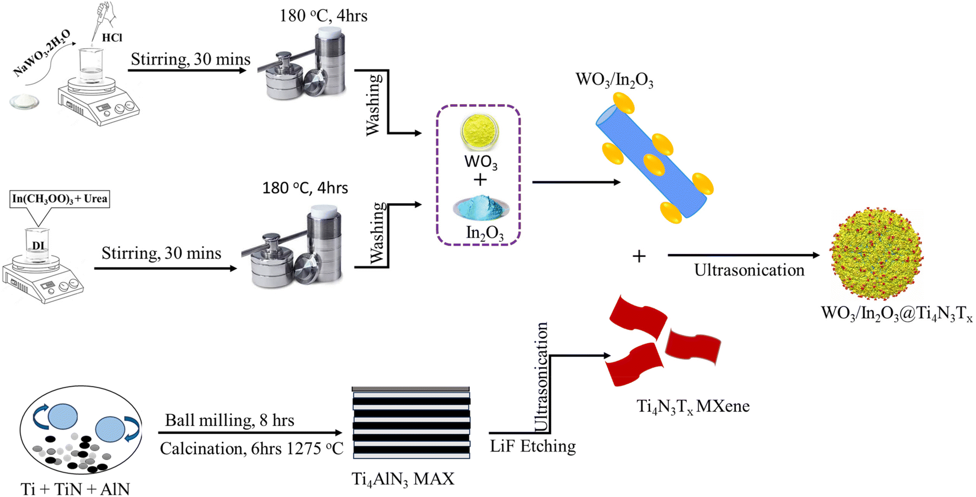 | ||
| Fig. 1 Schematic of the synthesis of the WO3/In2O3@ Ti4N3Tx composite. | ||
Precisely, 7.0 mmol Na2WO4·2H2O was dissolved in 20 mL of DI H2O. The pH of the solution was adjusted to 2 by a dropwise addition of 8 M HCl and continuously stirring for 30 min at room temperature (RT). The dispersed solution was hydrothermally heated at 180 °C in a stainless-steel, Teflon-lined 50 mL autoclave for 4 h and then left to cool to RT. The obtained suspension was then washed with DI H2O and ethanol several times and allowed to dry at RT.
![[thin space (1/6-em)]](https://www.rsc.org/images/entities/char_2009.gif) :2:1) were mixed via ball milling for 8 h, cold pressed into pellets and calcined at 1275 °C for 6 h under argon in a tube furnace and then crushed into fine powder. Precisely, 0.5 g of MAX was etched by soaking in a 10 mL mild etchant mixture of LiF and 9 M HCl for 12 h. The aluminium fluoride compound was removed by centrifugation at 350 rpm through washing with isopropanol until a pH of 6.5 and the resultant multilayered-Ti4N3Tx was obtained. This was followed by delamination in 10 mL TBAOH to obtain few-layered Ti4N3Tx. Excess TBAOH was removed via washing with isopropanol under centrifugation (Fig. 1).
:1 wt% ratio to form a homogeneous slurry that served as the working electrode. N-Methyl pyrrolidone (NMP) was used to dissolve this mixed slurry and form a sticky paste which was then coated onto a FTO glass surface and allowed to dry in air overnight.18 Visible light was flashed onto the working electrode during the study in a completely dark environment. The data collection was performed using the Gamry instrument (mode reference 1000E) operated at a frequency ranging from 10 kHz to 0.1 Hz with an AC and DC voltage of 10 mV rsm and 0.45 V vs. Eref, respectively. 0.8 V was applied at a step size of 2 mV to generate a Mott–Schottky plot at a frequency of 1000 Hz. Using the impedance potentiostat and frequency response analyzer (FRA) software, the charge carrier resistance was evaluated by electrochemical impedance spectroscopy (EIS). This was conducted using an applied voltage of 0.25 V and a current set between 100 mA and 100 nA. With the voltage set at 1.2 V, the photocurrent response was measured using chrono amperometry (Δt > 1 mV) to determine the lifespan of the photogenerated charge carriers.
:2:1) were mixed via ball milling for 8 h, cold pressed into pellets and calcined at 1275 °C for 6 h under argon in a tube furnace and then crushed into fine powder. Precisely, 0.5 g of MAX was etched by soaking in a 10 mL mild etchant mixture of LiF and 9 M HCl for 12 h. The aluminium fluoride compound was removed by centrifugation at 350 rpm through washing with isopropanol until a pH of 6.5 and the resultant multilayered-Ti4N3Tx was obtained. This was followed by delamination in 10 mL TBAOH to obtain few-layered Ti4N3Tx. Excess TBAOH was removed via washing with isopropanol under centrifugation (Fig. 1).
:1 wt% ratio to form a homogeneous slurry that served as the working electrode. N-Methyl pyrrolidone (NMP) was used to dissolve this mixed slurry and form a sticky paste which was then coated onto a FTO glass surface and allowed to dry in air overnight.18 Visible light was flashed onto the working electrode during the study in a completely dark environment. The data collection was performed using the Gamry instrument (mode reference 1000E) operated at a frequency ranging from 10 kHz to 0.1 Hz with an AC and DC voltage of 10 mV rsm and 0.45 V vs. Eref, respectively. 0.8 V was applied at a step size of 2 mV to generate a Mott–Schottky plot at a frequency of 1000 Hz. Using the impedance potentiostat and frequency response analyzer (FRA) software, the charge carrier resistance was evaluated by electrochemical impedance spectroscopy (EIS). This was conducted using an applied voltage of 0.25 V and a current set between 100 mA and 100 nA. With the voltage set at 1.2 V, the photocurrent response was measured using chrono amperometry (Δt > 1 mV) to determine the lifespan of the photogenerated charge carriers.
Results and discussion
Crystal structure
The obtained WO3 showed major diffraction peaks located at 23.1°, 23.5°, 23.6°, and 35.1°, which could be identified as the (002), (020), (202), and (222) planes, respectively, as shown in Fig. 2a. The crystalline structure of WO3 was assigned to the monoclinic form of crystalline WO3, in accordance with the ICDD card no: 04-002-3163, the space group P21/c. The primary growth direction of the WO3 crystal lattice was through the (202) facet, indicated by the intense diffraction peak at 2θ = 23.5°. Sharp and intense diffraction peaks showed an outstanding degree of crystallinity for the obtained WO3 nanoparticles, which agrees with literature reports.8 Powdered X-ray diffraction (PXRD) patterns of In2O3 showed major diffraction peaks at 21.5°, 30.6°, 33.1°, 35.4°, 37.7°, 41.8°, 45.6°, 50.9°, and 62.1° which could be identified as the (211), (222), (321), (400), (411), (332), (431), (440), and (631) diffraction planes, respectively (Fig. 2a). ICDD card no: 04-006-0857 ascribed the material to the cubic form of crystalline In2O3, with the space group Ia![[3 with combining macron]](https://www.rsc.org/images/entities/char_0033_0304.gif) (a, b, c = 10.1260 Å). The obtained polymorph of In2O3 with a body-centered-cube (bcc) structure has an optimum band-edge position, excellent conductivity and outstanding photoelectrochemical stability, making it suitable for photocatalytic applications (Fig. 2a).19
(a, b, c = 10.1260 Å). The obtained polymorph of In2O3 with a body-centered-cube (bcc) structure has an optimum band-edge position, excellent conductivity and outstanding photoelectrochemical stability, making it suitable for photocatalytic applications (Fig. 2a).19
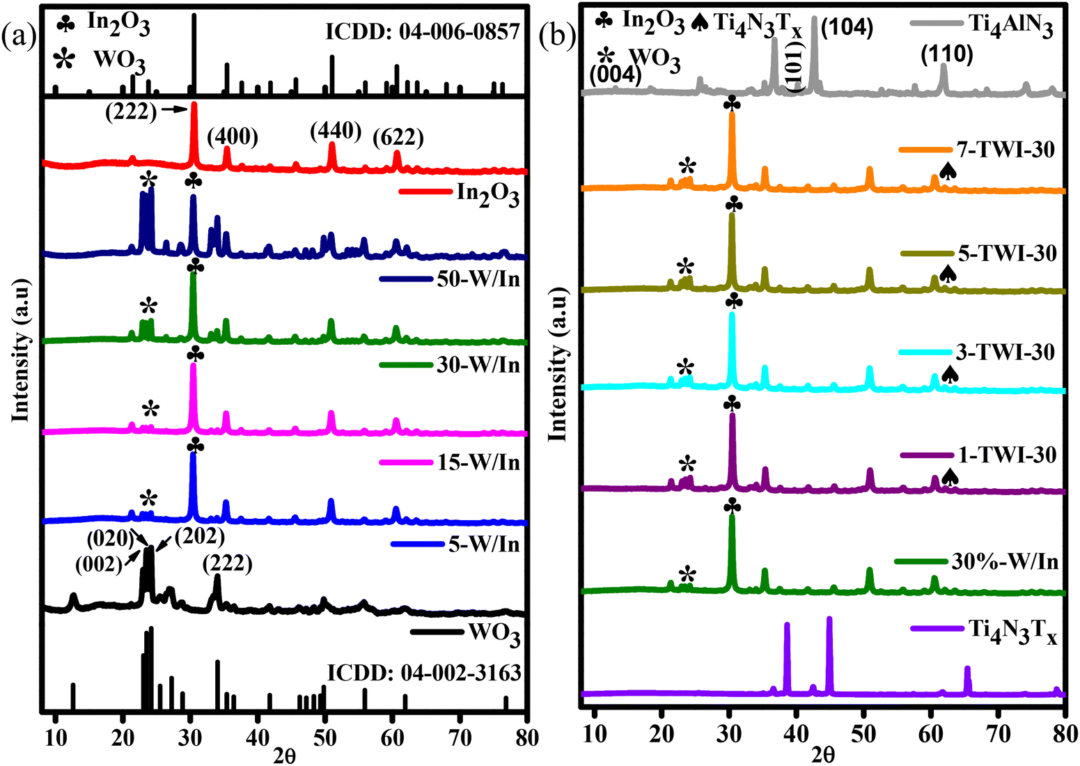 | ||
| Fig. 2 XRD patterns for (a) pristine WO3, In2O3, and binary nanocomposites; (b) Ti4AlN3 MAX, Ti4N3Tx MXene and ternary nanocomposites. | ||
In Fig. 2a, all major diffraction peaks belonging to pristine WO3 (★) and In2O3 (♣) were observed in binary composites. There was an increased diffraction peak intensity for binary composites compared to pristine materials. Adding WO3 into In2O3 promoted crystal growth, changing their initial obtained monoclinic and cubic phases into a general hexagonal phase structure.10,20 The improved crystalline phase regulation optimizes the bandgap and significantly impacts charge carrier recombination inhibition.21 However, further increase of WO3 content beyond 30% resulted in the loss of crystallinity. Transformation of the crystalline phase of the binary nanocomposite into the amorphous nature at 50% WO3 was indicated by the reduction in the sharpness of characteristic peaks (Fig. 2a). This was attributed to the masking effect induced by the phase structure of WO3 onto the In2O3 crystal structure.8 Hence, 30% WO3 (WI-30) content in the composite was therefore used for the fabrication of ternary composites due to its outstanding degree of crystallinity.
The XRD patterns of Ti4AlN3 MAX and Ti4N3Tx MXene are displayed in Fig. 2b and the extract of the patterns (5–20° (2θ)) is shown in the ESI (Fig. S1†). The synthesized Ti4AlN3 MAX phase showed peaks at approximately 5.8°, 13°, 18°, 36°, 44° and 62° which corresponded to the (002), (004), (103), (101), (104), and (110) hexagonal phases of Ti4AlN3, respectively (Fig. 2b and S1†). These peaks matched the reference Ti4AlN3 phases reported in the literature.22 The aluminium layer was etched out following an in situ prepared HF from LiF and HCl treatment. The (103) peak disintegrated into reflection peaks (◆) in Ti4N3Tx, as shown in Fig. S1.† Consequently, the (002) peak broadened and shifted from 5.8° to 5.4°, indicating the change in the lattice parameter (c-LP) of the cell. This is evident by the shift in d-spacings from 6.73 Å in Ti4AlN3 MAX to 7.47 Å. Similarly, lattice parameter changes in the unit cell of Ti4N3Tx were due to the introduction of functional groups (–O, –OH, –F) and Li+ intercalation between the interspaces. In ternary nanocomposites, PXRD patterns for 1, 3, 5, and 7 wt% showed a Ti4N3Tx (110) peak (/) along with other peaks belonging to WO3 (★) and In2O3 (♣),further confirming a successful fabrication of the TWI-30 ternary heterojunction (Fig. 2b). However, 3-TWI-30 showed the best crystallinity.
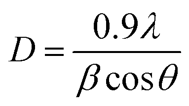
Herein, the PXRD results ascertained the successful synthesis of all nanomaterials. Using the Scherrer equation, grain sizes (WO3, In2O3, WI-30, and 3-TWI-30) in the nanostructure were calculated using their diffraction peak broadening in accordance with eqn (1):23
 | (1) |
Raman findings shown in Fig. S2a and b† ascertain vibrational modes in the as-synthesised material. The phonon bands of WO3 confirmed PXRD findings which showed sharp well-defined peaks at 806, 717, 326, 269 and 135 cm−1 corresponding to the monoclinic phase of WO3 (Fig. S2a†). The band peaks at 717 and 806 cm−1 were assigned to O–W–O stretching modes while 326, 269 and 135 cm−1 to O–W–O bending vibrations.24 The cubic In2O3 structure belongs to the space groups Ia3 and Th7. Two types of cations are present in the structure: 24 (point groups) In3+ with the point symmetry C2 and 8 (side groups) In3+ with the side symmetry S6.25 In a body-centered cell, the existing 48 oxygen atoms retain the C1 site symmetry and are arranged in general places (e). Such a structure is described by the following vibration modes as given in eqn (2):25
| 4Ag + 4Eg + 14Tg + 5Au + 5Eu + 16Tu | (2) |
While the Tu vibrations are both infrared active and Raman inactive, the Ag, Eg, and Tg symmetry vibrations are both Raman active and infrared inert. However, Au and Eu vibrations are both infrared and Raman inactive. Unambiguous Raman spectra signatures of the cubic In2O3 structure with phonon modes at 305, 363, and 495 cm−1 were also observed for our synthesized sample and indexed to E2g, Ag, and Eg with reference to a literature report (Fig. S2a†).26 The nanocomposite structures comprised of individual pristine WO3 (*) and In2O3 (♣) phonon modes (Fig. S2a†). The binary peaks slightly broadened, became less intense and slightly shifted to higher wavenumbers. These slight shifts were related to the increase in the length of the In–O bond induced by substitution of In3+ by W6+. Additionally, the observed small line width in each spectrum contributed to the nanocrystalline structure with good crystallinity as observed in the XRD patterns.
Raman spectra for MAX and MXene were labelled after Gaussian and Lorentzian function fitting (Fig. S2b†). The peaks were indexed as ω2 (134.6 cm−1) and ω9 (558.6 cm−1) which belong to E1g group vibrations. They contained in-plane modes of Ti and N atoms. Similarly, ω4 (212.5 cm−1), ω6 (251.2 cm−1), ω7 (378.1 cm−1), and ω8 (548.5 cm−1) modes corresponded to A1g symmetry out-of-plane vibrations of Ti and N atoms. These peaks were present in the Ti4AlN3 MAX phase while ω4, ω6, ω7, and ω8 (548.5 cm−1) modes were observed in the Ti4N3Tx spectrum. After etching Al, a reduction in peak intensity was observed. The peaks shifted to lower energy. The induced structural surface moieties during etching and delamination processes resulted in peak broadening with an increased interlayer d-spacing.27 Addition of Ti4N3Tx into the binary nanocomposite further resulted in increased peak intensities. The observed optical phonon modes of WO3, In2O3 and Ti4N3Tx in the nanocomposite suggested the effective development of 3-TWI-30 which indicated a clear fabrication of a ternary nanocomposite (Fig. S2a†).
Functional groups
Functional groups of the pristine and nanocomposites were further ascertained from the FTIR spectrum in Fig. S2c.† Stretching and bending modes which correspond to the W–O vibrations of the material were seen in the FTIR spectrum of pure WO3 as reported in the literature.28 The peak observed at 3429 cm−1 was due to the stretching vibration of the surface O–H group. The minor peak at 1624 cm−1 was the W–OH vibration and the strong peak at 766 cm−1 was ascribed to the W–O–W bridging mode.29 Similarly, peaks at 440 and 557 cm−1 were attributed to In–O stretching vibrations in cubic In2O3. The bands at 602 and 827 cm−1 were characteristic of In–O bending vibrations in In2O3.28 Broad characteristic peaks at 557 cm−1 and 827 cm−1 present in In2O3 corresponded to the β-In2O3 phase. Additionally observed peaks at 3424 and 1646 cm−1 belonged to the stretching and bending vibrations of O–H bands.30The Ti4AlN3 MAX phase exhibited a broad peak at ∼675 cm−1, which was ascribed to a Ti–Al–N vibration as per literature reports.31 After etching and delamination to Ti4N3Tx, disappearance of this broad spectral feature and formation of a new peak at 537 cm−1 were observed. This was attributed to the successful removal of the Al layer and formation of a new Ti–N vibration. Notably, in the exfoliated Ti4N3Tx spectrum, a much broader peak centered at ∼3424 cm−1 was observed to be a characteristic O–H/N–H stretch. Similarly, formation of a new peak at 537 cm−1 was observed which could be ascribed to the Ti–F stretching. This was related to the hydrophilic nature of Ti4N3Tx due to terminal functional groups (O–F, Ti–F, OH, and NH).
Furthermore, FTIR spectra for binary nanocomposites comprised of prominent peaks of WO3 and In2O3 (Fig. S2c†).9 The vibrational peak intensity of Ti4N3Tx belonging to Ti–N, Ti–F was observed in the case of the ternary nanocomposite. Concomitantly, a broad band and sharp intense peak at 3424 and 1637 cm−1 were assigned to the υ(O–H) stretching modes as a result of δ(H–O–H) bending vibration modes, respectively. This O–H stretching showed a much broader peak in the ternary nanocomposite due to the contribution of the O–H functional group from Ti4N3Tx. All surface functional groups belonging to Ti4N3Tx (O–F, Ti–F, OH, and NH) were observed in the ternary nanocomposite, indicating the successful addition of Ti4N3Tx to the binary nanocomposite.
Morphology
The shape and microstructure of the as-synthesized materials were investigated using SEM and TEM as shown in Fig. S3† and Fig. 3. In Fig. S3a,† 2D WO3 nanoparticles exhibit a rod-like morphology and their composition was confirmed by EDS to be W and O. The SEM image of pristine In2O3 nanoparticles in Fig. S3b† shows a cube-like morphology, which agglomerated to exhibit a flower-like comb.32 Their EDS spectrum confirmed the presence of In and O. In Fig. S3c,† the 2D WO3 nanoparticles were finely disseminated over In2O3 nanosheets resulting in the formation of the WO3/In2O3 binary nanocomposite. This was further confirmed by the EDS spectrum indicating the elemental composition to be W, In and O. Fig. S3d and e† show the SEM images of Ti4AlN3 and Ti4N3Tx MXene, respectively. The SEM images of Ti4AlN3 MAX (Fig. S3d†) and Ti4N3Tx in Fig. S3e† display a morphological change before and after etching.33 Their EDS analysis was consistent with previous literature reports, which showed the presence of Ti, N, Al and O in the MAX phase.34 The removal of Al in MXene was confirmed by the disappearance of the Al peak in the EDS spectrum (Fig. S3e†). In Fig. S3f,† there was an over-layer of the Ti4N3Tx structure on the binary nanocomposite as evidenced by the appearance of a disintegrated layer. The elemental composition was confirmed by EDS analysis to be In, W, N, F, and O. The elemental mapping for the 3-TWI-30 ternary composite is indicated in Fig. S4† to include Ti, W, In, N, O and F.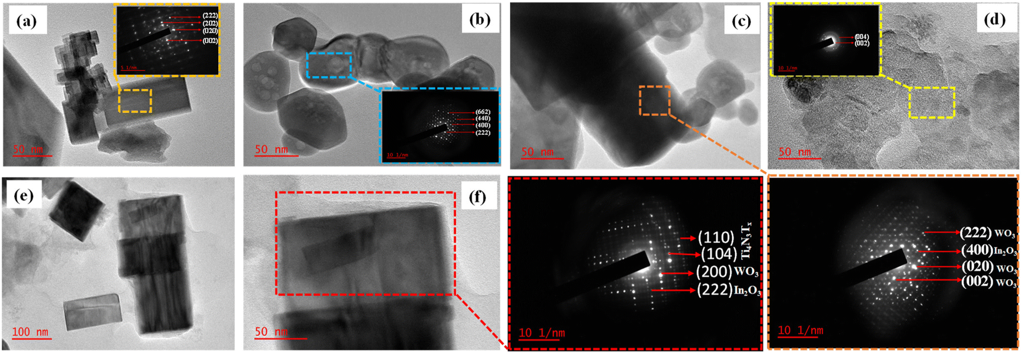 | ||
| Fig. 3 TEM images for (a) WO3, (b) In2O3, (c) WI-30, (d) Ti4N3Tx MXene, (e) 3-TWI-30 ternary and (f) HRTEM 3-TWI-30 ternary heterostructures. | ||
Fig. 3a shows TEM images of pristine WO3 with a 2D rectangular shape-like structure.35 In2O3, in Fig. 3b, shows a body-centered cubic morphology. Fig. 3c confirms the formation of a binary composite with In2O3 cubes decorated onto the rectangular-shaped structure of WO3. Ti4N3Tx MXene in Fig. 3d shows a nanosheet-like morphology.36 The formed ternary composite in Fig. 3e was confirmed by the layering of Ti4N3Tx MXene nanosheets onto the rectangular WO3. The cubic In2O3 is not clearly shown. This is due to the masking effect of WO3. The SAED patterns for all the materials were indexed by calculating the d-spacings for the individual material using the ImageJ software. The SAED patterns for WO3 observed were (222), (202), (020) and (002) (Fig. 3a inset). This is in agreement with the XRD pattern analysis.35 Similarly, the In2O3 cubic structure indicated the SAED sets of (622), (440), (400) and (222) as shown in Fig. 3c inset. These were further confirmed in the binary composite with those belonging to WO3 dominating as indicated in Fig. 3c. Ti4N3Tx exhibits two distinct crystal planes belonging to (002) and (004) (Fig. 3d inset).
Furthermore, the presence of Ti4N3Tx MXene nanosheets on WO3/In2O3 confirms the role of Ti4N3Tx MXene as the electron sinks = in separating electrons from the CB of WO3. The formation of the ternary nanocomposite was further confirmed by the SAED sets of (110), (104), (200), and (222) to be a combination of the three as shown in Fig. 3e and HRTEM in Fig. 3f.
Elemental composition and chemical states
The chemical composition, oxidation states and the electron migration route of the heterostructure were ascertained by analysing the change in binding energy using X-ray photoelectron spectroscopy (XPS) (Fig. S5† and Fig. 4). | ||
| Fig. 4 XPS spectra of the as-prepared materials (a) W 4f, (b) In 3d (c) O 1s; (d) Ti 2p and the intensity for (e) Al 2p and (f) N 1s. | ||
The survey spectra of the Ti4AlN3 MAX phase, Ti4N3Tx MXene, WO3, In2O3 nanoparticles, WI-30, and 3-TWI-30 heterostructures are displayed in Fig. S5† (and its extract) presenting Ti, N, W, O, In, and Al elements.
The F element observed on the Ti4N3Tx MXene results from etching with LiF salt and HCl. The W 4f spectrum shown in Fig. 4a has two evident peaks at 35.3 and 37.4 eV, ascribed to W 4f7/2 and W 4f5/2 of WO3, respectively. In the WI-30 and 3-TWI-30 heterostructures, these W 4f peaks slightly shifted toward lower binding energy in comparison to pristine WO3 nanoparticles implying electron depletion on WO3. The In 3d spectrum in Fig. 4b consists of a doublet at binding energies of 452.2 eV for In 3d3/2, and 444.6 eV for In 3d5/2 which shifted to higher binding energy in WI-30 due to electron accumulation.37Fig. 4c shows a high-resolution O 1s spectrum for pristine WO3, In2O3, and their composites, Ti4N3Tx MXene and Ti4AlN3 MAX with two peaks at 530.3 and 532.1 eV. The intense peak at 530.3 eV is attributed to the lattice oxygen in WO3 and In2O3 species characteristic of metal oxides, and the weak peak at 532.1 eV could be due to the adsorbed oxygen.38 The 530 eV peak is more intense and broader in indium oxide than in the WO3 photocatalyst indicating more oxygen vacancies in In2O3.10 O 1s for Ti4AlN3 MAX and Ti4N3Tx MXene was fitted, and three sub-peaks observed were related to Ti–O (528 eV), Ti–OH (532 eV) and adsorbed moisture (533 eV). Fig. 4d indicates the observed Ti 2p peaks for both Ti4AlN3 and Ti4N3Tx nanocomposites. A more informative understanding of the prevailing chemical state present in MAX and MXene can be obtained from the Ti 2p spectra. Two transition splits are produced by the Ti 2p spin–orbit splitting within the range of 453–460 eV forming Ti 2p3/2 and the peaks from 460 to 466 eV are due to the Ti 2p1/2. A similar peak of Ti2+ at 455.0 eV, and at 456.9 eV (Ti3+) and 458.6 eV (Ti4+) in TiN are also observed in the Ti4AlN3 MAX. After Al3+ exfoliation, there is a disappearance of the original Ti2+ feature in Ti4N3Tx MXene. The observed peaks at 457.0 and 458.5 eV are ascribed to Ti3+ and Ti4+. Additionally, the Ti3+ peak at 457.0 eV in the Ti4N3Tx MXene spectrum broadened compared to the MAX phase (Fig. 4d). The similarity in electronegativities exhibited by both Ti and Al (1.54 for Ti; cf. 1.61 for Al) indicates the likelihood of a shared Ti–Al bonding structure in the Ti4AlN3 MAX phase to include Ti2+, Ti3+, and Ti4+ as well as Al3+, as observed in its XPS spectrum.31 However, the two terminal Ti layers in the 7-atom layer Ti4N3Tx sheets exhibit a Ti4+ oxidation state in Fig. 4d. The Ti4+ peak is observed in the Ti 2p spectrum at 459 eV with a slightly lower energy Ti4+ peak in the Ti4N3Tx MXene due to the Ti4+ environment consisting of both Ti–O and Ti–N characters. Similar to the Raman and FTIR spectroscopic data, these XPS Ti 2p data also indicate the formation of surface oxide (Tx = O and/or OH). Two inner Ti layers in the 7-atom layer Ti4N3Tx sheet formally are in a Ti3+ oxidation state and are bound only via Ti–N interactions in both the Ti4AlN3 MAX and Ti4N3Tx MXene phases. The shift to a higher binding energy observed in Ti 2p in 3-TWI-30 is due to an increased electron density flowing from the CB of WO3 in WI-3O.37,39Fig. 4e and f illustrate the distinct variations in the spectrum areas for Al 2p and N 1s for the Ti4AlN3 MAX and Ti4N3Tx MXene phases, respectively. The Al peak position (about 75 eV) in Fig. 4e is in line with an Al3+ environment in the Ti4AlN3 MAX phase. This peak decreases in intensity and shifts to lower binding energy after etching. This is due to distortion of the Ti–Al–N bond and formation of new Ti–N weak van der Waal bonds in the Ti4N3Tx MXene. The N 1s spectrum for the Ti4AlN3 MAX phase in Fig. 4f exhibits an intense peak at 397.3 eV which is consistent with the peaks present from a metal nitride bond. After Al removal, an increase in peak intensity was observed with a subsequent shift to a lower binding energy in Ti4N3Tx MXene. However, after addition of the Ti4N3Tx MXene, the peaks shifted to higher binding energy. The N 1s in Ti4N3Tx MXene shifted to lower binding energy and broadened. This is relatable to the weakened bond due to the Al removal.37 However, in 3-TWI-30, the N 1s peak becomes more broader and uniformly distributed. This is due to the effect of accepted electrons from WI-30.40
Optical properties
UV-vis spectroscopy was used to examine optical band edge absorption, bandgap and emission band peaks of the synthesized materials. Pristine WO3 and In2O3 (Fig. 5a) displayed relatively lower absorption intensities in the visible light region with absorption edges at 520 and 420 nm, respectively. | ||
| Fig. 5 (a and b) UV-vis absorption spectra and (c and d) Tauc plots of the as-prepared materials. | ||
Introduction of WO3 nanoparticles into the In2O3 photocatalyst improved the photon absorption of the photocatalyst. A red shift was observed upon increasing the WO3 content in the binary composite from 5 to 30% with a maximum absorption at 470 nm (WI-30).
A further increase in WO3 content showed a blue shift in absorption.
This could be attributed to the masking effect of WO3 on In2O3. Ti4N3Tx showed no absorption edge across the 200–800 nm, which was related to its metallic structure (Fig. 5b). The observed absorption edge range for ternary nanocomposites was 480 nm to 430 nm with 3-TWI-30 absorbing within the visible range (463 nm) (Fig. 5c).
E g for the as-synthesized photocatalysts was examined using the Kubelka–Munk eqn (3):
| (αhv) = A(hv − Eg)1/n | (3) |
The introduction of WO3 nanoparticles onto the In2O3 photocatalyst narrowed the Eg of nanocomposites, hence promoting visible light absorption, a first requirement step in a photocatalytic reaction.42 Therefore, the constructed WI-30 binary heterojunction composite vastly improved the utilization of broad light absorption in comparison to pristine materials. Upon fabrication of the ternary nanocomposite, there was a visible change in Eg with 1, 3, 5 and 7 wt% (TWI-30) having an Eg of 2.36 eV, 2.33 eV, 2.56 eV and 2.55 eV, respectively (Fig. 5d). A ternary nanocomposite, made up of 3 wt% MXene, showed the lowest Eg of 2.33 eV, suggesting superior absorption capabilities to the other MXene loading wt%.
XPS valence band (VB) analysis further deduced the changes in the position of the energy band edges due to the bandgap position shift. The XPS VB spectrum for WO3 in Fig. 6a derives its VB potential (EVB, vs. vacuum) to be 2.98 eV (vs. vacuum), while that for In2O3 was 2.03 eV (vs. vacuum) (Fig. 6b).43 Based on their respective Eg values, the conduction band potentials ECB (vs. vacuum) were estimated to be 0.85 and 2.03 eV, respectively. The extrapolated XPS EVB average in WI-30 and 3-TWI-30 was 2.21 and 2.12 eV (vs. vacuum), respectively as shown in Fig. 6c and d. These confirm the successful effect of heterostructure formation on influencing band potentials and band edge deduction as summarized in Table 1 and Fig. 7, respectively.
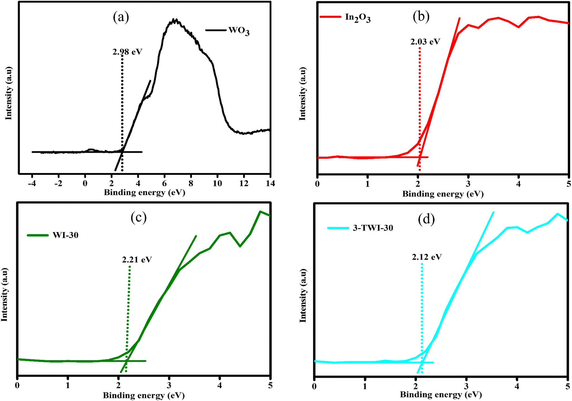 | ||
| Fig. 6 XPS VB spectra for (a) WO3, (b) In2O3, (c) WI-30 and (d) 3-TWI-30. | ||
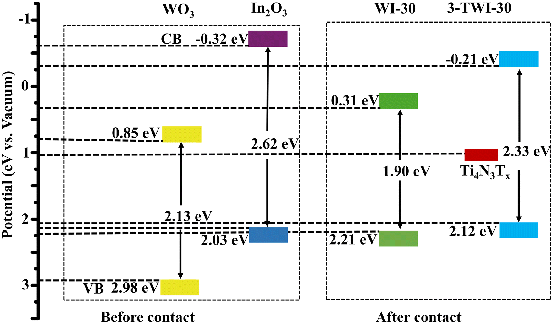 | ||
| Fig. 7 Band edge position diagrams of the synthesized semiconductors based on the XPS data. | ||
| Sample | Absorption edge (nm) | Bandgap (eV) | XPSVB (eV) | XPSCB (eV) |
|---|---|---|---|---|
| WO3 | 416 | 2.13 | 2.98 | 0.85 |
| In2O3 | 455 | 2.62 | 2.03 | −0.32 |
| WI-30 | 470 | 1.90 | 2.21 | 0.31 |
| 3-TWI-30 | 463 | 2.33 | 2.12 | −0.21 |
Photoelectrochemical studies
The photoluminescence intensities for pure WO3 and In2O3 photocatalysts exhibited the strongest PL peaks in the range of 340 nm–360 nm at an excitation wavelength of 350 nm, indicating the highest recombination rate of photoinduced carriers (Fig. 8a and b). | ||
| Fig. 8 (a and b) PL spectra, (c and d) EIS Nyquist plot of the as-prepared materials, inset: Randles–Ershler equivalent circuit. (Cdl = double layer capacitance, RCT = charge transfer resistance, and Rs = solution resistance) and (e and f) photocurrent response of the pristine and nanocomposites. | ||
After loading WO3 nanoparticles onto In2O3, a reduction in the PL intensities was observed for binary nanocomposites in comparison to pristine WO3 with WI-30 recording the least peak intensity.
A decrease in PL intensity signified that there was a reduction in photoinduced charge carrier recombination rate.44 The formation of the heterojunction contributed to the change in the charge carrier transfer route. Similarly, reduction in e−/h+ recombination could be as well attributed to improved crystallinity of composites. The smaller the crystal size, the shorter the diffusion pathways of charge carriers as well as improved spatial separation of e−/h+.45 Consequently, increased content of WO3 results in masking of In2O3 which caused an increase in the recombination rate of nanocomposites. A consequential reason for the observed increase in PL intensity is the increase in WO3 content to 50%.
MXenes are metallic compounds with high conductivity properties, therefore exhibiting efficient charge transfer mobility.46 Hence, upon fabrication with Ti4N3Tx, a much lower PL intensity was recorded, with 3-TWI-30 reporting the lowest PL intensity (Fig. 8b). The reduced PL intensity suggests the successful formation of a Schottky barrier between the WI-30 heterostructure and MXene.46 The Schottky barrier, therefore, acted as a shuttle for e− from WI-30 to Ti4N3Tx. In addition to the metallic nature of the MXene, a reduction in PL intensity might be related to the porous nature of Ti4N3Tx which acted as electron traps further separating and stabilizing photoseparated electrons from active holes. However, MXenes can behave as recombination centres at high Ti4N3Tx loading, evidenced by increased recombination rates as observed in 5-TWI-30 and 7-TWI-30 composites.
Considering the diameters of the semicircles, the Nyquist plots reveal the generated charge carrier resistance (Fig. 8c and d). The Nyquist plot has the imaginary impedance value (Z′′) and the real impendence value (Z′), which show the charge transfer resistance (RCT) fitted by the Randles–Ershler equivalent circuit (Fig. 8c and d: inset). A smaller arc radius shows an efficient charge transfer and a more effective separation of photoinduced charge carriers.47
As shown in Fig. 8c, pristine WO3 and In2O3 photocatalysts exhibited largest curves, an indication of a high charge transfer resistance, 41.2 and 42.3 Ω, respectively, attributed to the lower interfacial charge transfer and increased charge carrier recombination rate.
Upon binary fabrication, an increase in curves and later reduction with WI-30 reporting the smallest curve with a resistance of 33.0 Ω was observed. WI-5, WI-15, and WI-50 exhibited 38.5, 70.5 and 71.5 Ω, respectively. There was a significant reduction in charge-transfer resistance upon incorporating the appropriate amount of WO3 into the intrinsic structure of In2O3. The induced interfacial reaction mechanism within 30% WO3 and In2O3 contact leads to faster and more efficient charge separation and transfer.
Further addition of Ti4N3Tx to the WI-30 binary nanocomposite reduced the charge resistance, with 3-TWI-30 reporting the least 31.9 Ω resistance, while 1-TWI-30, 5-TWI-30 and 7-TWI-30 exhibited 41.9, 49.6 and 49.0 Ω resistance, respectively. This was related to the metallic nature and charge transfer capacity of MXenes which offer stable landing sites for photogenerated electrons. Similarly, in 2015, Yan et al. reported that oxygen vacancies of In2O3 in the ternary composite facilitate the formation of inter-bandgap states below the CB minimum responsible for the extra charge carriers facilitating an increased e− lifetime. They bind electrons to states of shallow defects.48 An extended lifetime would provide photogenerated holes in the VB a longer time to migrate toward the electrode/electrolyte contact and participate in the oxidation process.
Photocurrent response was recorded to explore interfacial electron–hole separation and transfer (Fig. 8e and f).49 Five cycles of on and off of visible light irradiation were performed to record the transient photocurrent responses of pure WO3, In2O3, and nanocomposites with WO3 exhibiting the lowest photocurrent response. Photocurrent intensities of WI-30 photocatalysts were most improved and gradually reduced upon increasing the WO3 content (Fig. 8e). Transient photocurrent of the WI composite catalyst was distinctly enhanced compared to that of pure WO3 or In2O3. Introduction of WO3 nanoparticles enhanced the separation efficiency of e−/h+ in WI up to a given limit, after which, it masked In2O3 resulting in the reduction of photocurrent response.
Similarly, in 2021, Banerjee et al. reported that 8.5 wt% of NiO could cover InTaO4 and offset its light absorption.50 In 2023, Chico-Vecino et al. also prepared the WO3/In2O3 composite and observed the same effect.10 Upon MXene introduction, an increase in photocurrent density was observed with 3-TWI-30 exhibiting the highest photocurrent density (Fig. 8f). This was due to the increased light absorption ability of the ternary nanocomposite and a tighter connection between WI-30 and Ti4N3Tx leading to more efficient separation and flow of e−/h+.51 High photocurrent response minimizes photocorrosion of e−/h+. In turn, their recombination rate is minimized.
A Mott–Schottky study was conducted to deduce band edge potentials and explore the charge transfer pathways in Fig. S6a.† The deduced flat band potential from the Mott–Schottky plot was employed in the determination of the band edge structure and pathways opted by e−/h+ in semiconductor materials. The X axis intersections in the Mott–Schottky plots yielded values of the flat-band potentials. Notably, a shift in the flat band potentials was observed in the composites with the WI-30 binary nanocomposite exhibiting higher values compared to pristine materials (Fig. S6c and d†). This indicated an excellent interfacial e− migration. The individual oxides demonstrated positive slopes on their Mott–Schottky curves suggesting n-type semiconductors (Fig. S6a and b†).
Accordingly, the Fermi level for n-type semiconductors is estimated to be 0.1 V to 0.3 below the CB.52 Based on this assumption, flat band potential (EFB) values were used in calculating the CB potential for each material. Using the Nernst equation, the obtained EFB values against the Ag/AgCl scale were changed to the NHE scale, as shown in eqn (4).
 | (4) |
| EVB = Eg + ECB | (5) |
Through the determined bandgap and VB position, the CB and energy levels of WO3 and In2O3 were deduced to be −0.246 and −1.204 V while their VBs were 1.884 and 1.416 V, respectively, as further indicated in Table S2.† Additionally, MS plots were utilized to evaluate the carrier concentration (ND, donor carriers for an n-type semiconductor) for the synthesized photocatalysts, according to eqn (6):
 | (6) |
The dielectric constants for WO3 and In2O3 were obtained from the literature as 5.03 and 8.9, respectively.53,54 The calculated ND from the individual MS slope in Table S2 provided in the ESI† was 11.05 × 10²¹, 6.25 × 10²¹, 2.70 × 10²¹ and 7.83 × 1021 cm−3 for WO3, In2O3, WI, and TWI, respectively. The lowest MS slope in WO3 results in the highest ND, while 3-TWI-30 showed a better ND. Moreover, the ND value increased as the Ti4N3Tx loading increased, an indication of increased induction in charge carrier mobility.
To identify the formed reactive species accountable for the breakdown of organic pollutants in wastewater, the CB and VB potentials for the synthesized materials were compared with O2/˙O2− and OH−/˙OH generation potentials. This was based on the energy band edge diagram deduced from Mott–Schottky analysis (Fig. S6†). The CB of In2O3 had a redox potential capable of producing superoxide radicals (ECB = −1.66 V; E(O2/˙O2−) = −0.33 V vs. NHE). Similarly, WO3 has a VB potential capable of producing hydroxyl radicals (EVB = 1.88 V; E(OH−/˙OH) = 0.96 V) as indicated in Fig. 9.
 | ||
| Fig. 9 Proposed band edge diagram. | ||
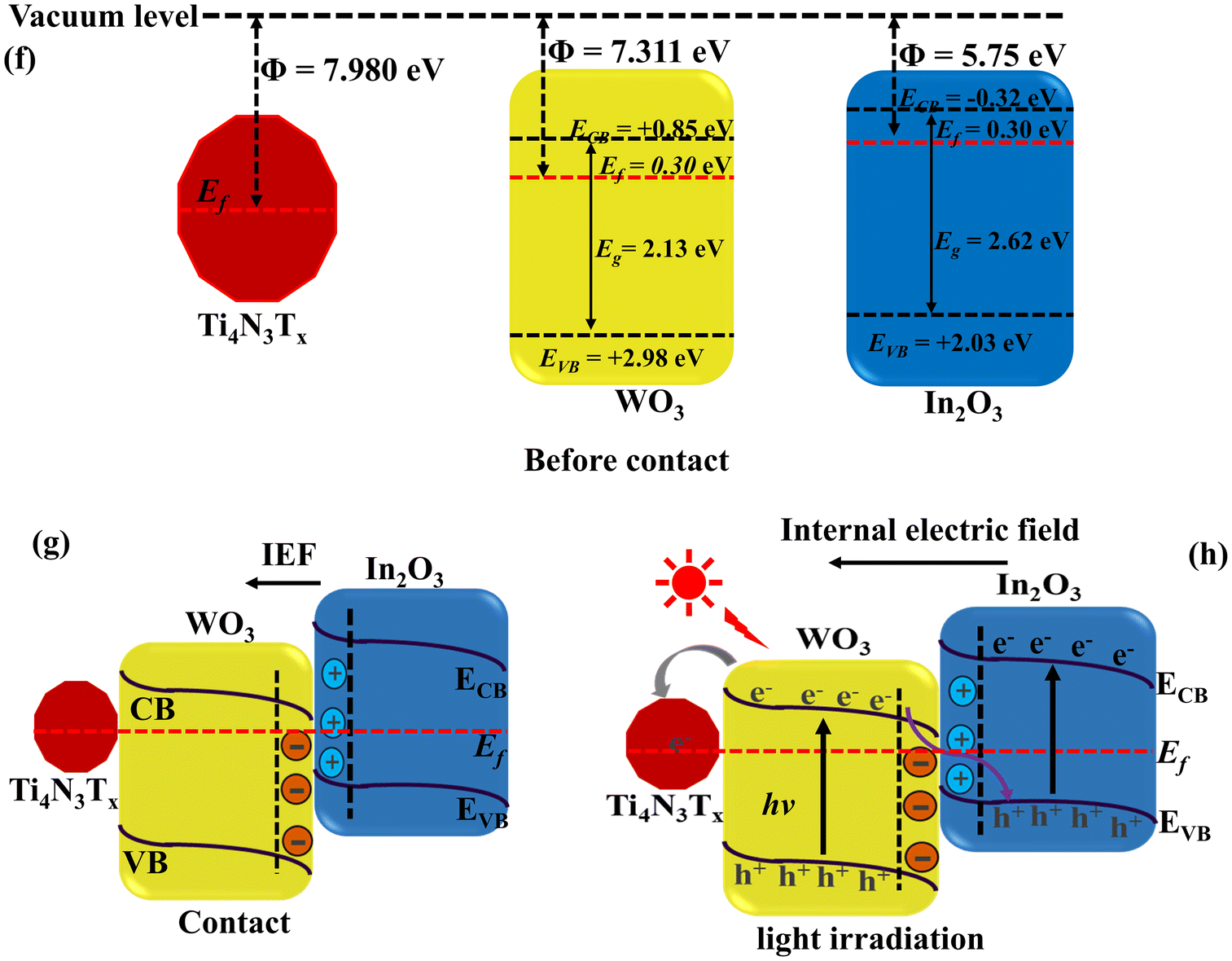
The work function plays a key role in determining the charge transfer mechanism at the interface of the 3-TWI-30 S-scheme structure.
Fig. 10 shows the obtained work function of WO3 (a), In2O3 (b), Ti4N3Tx (c), WI-30 (d) and 3-TWI-30 (e) obtained via XPS and the sketches of the internal electric field and charge transfer (Fig. 11f–h). In the XPS measurement, the energy transformation is given by a relationship of the solid sample: hν = Ek + Eb + Φ (hν is the incident photon energy, Ek is the photoelectron kinetic energy, Eb represents the electron binding energy, and Φ gives the sample's work function).55 The difference in the work function gives a different contact potential energy (ΔV) = Φ − φ (φ is the work function of the instrument and the value is 5.05 eV). These have a net effect on the kinetic energy of the free electrons with a concomitant change in the electron binding energy. XPS detects the changes in the binding energy while the distance between the inflection points (IP) allows for the determination of ΔV (Fig. 10(a–e)). Φ could then be calculated. The work functions of WO3, In2O3, Ti4N3Tx, WI-30 and 3-TWI-30 were determined to be 7.311, 5.75, 7.980, 6.13, and 5.919 eV, respectively.
 | ||
| Fig. 10 Work function of all as-synthesized materials measured by VB XPS and sketches of the internal electric field and charge transfer. | ||
 | ||
| Fig. 11 Internal electric field and charge transfer. | ||
An S-scheme structure was constructed based on the obtained band edges (VB, CB), work functions and Fermi levels. In2O3 forms a reduction photocatalyst (RP) with higher CB and VB positions relative to WO3 as an oxidation photocatalyst (OP). Upon closer contact, electrons in In2O3 diffuse to WO3 resulting in the creation of electron depletion and accumulation layers in In2O3 and WO3, respectively (Fig. 11f).
WO3 becomes positively charged while In2O3 becomes negatively charged.56 The flow of charge carriers, in consequence, induces an internal electric field (IEF) flowing from In2O3 to WO3 accelerating the photoinduced electron transfer from WO3 to In2O3. When WO3 and In2O3 comes into contact, an equilibration occurs as the Fermi levels align in the position of the least energy. This is achieved through an upward shift in the In2O3 Fermi level and a downward shift in the WO3 Fermi level.57 The band bending, IEF and coulombic attraction promote recombination between photogenerated electrons in the CB of WO3 with holes in the VB of In2O3. Consequently, the potent photogenerated electrons in the CB of In2O3 and the holes in the VB of WO3 are preserved for photocatalytic processes, while the ineffective electrons in the WO3 CB and the holes in the In2O3 VB are eliminated (Fig. 11g).58 The observed interfacial charge-transfer behaviour of the In2O3/WO3 heterojunction accords with the XPS data, in agreement with the S-scheme heterojunction mechanism.59 The positioning of Ti4N3Tx onto WO3 is based on its work function and its Fermi level, where the minimum energy is required for adjusting the Fermi level alignment during equilibration with that of the heterostructure (In2O3/WO3). Given the larger work function of WO3 and its lower Ef closer to that of Ti4N3Tx, the photoinduced electrons can easily flow from the WO3 heterojunction to Ti4N3Tx (Fig. 11h). The weak van der Waal forces facilitate the adsorption of Ti4N3Tx onto the photocatalyst surface, where it serves as an electron-trapping center.60
Conclusion
In conclusion, an S-scheme heterojunction photocatalyst was successfully fabricated based on the combination of an oxidative photocatalyst WO3 with In2O3 and Ti4N3Tx MXene as co-catalysts. The pristine materials were prepared via solvothermal synthesis, with the binary and ternary composites being prepared via an electrostatic assembly followed by calcination. The photoelectrochemical analysis of the as-synthesized materials showed that WO3 loaded onto In2O3 showed improved photoelectrochemical properties. There is a masking effect induced by WO3 at loadings above 30 wt%. Furthermore, the introduction of the MXene co-catalyst enhanced the properties of the ternary composite. In addition, the fabricated S-scheme multijunction photocatalyst (In2O3/WO3@Ti4N3Tx) has a sufficient light harvesting capability and retained reduction and oxidative potentials for generating photoinduced reactive radicals with potential in energy and environmental remediation. The synthesized photocatalyst is recommended for application in the degradation of emerging pollutants (ARVs) in water.Author contributions
Antony O. Onjwaya: acquisition of data, analysis and/or interpretation of data, and writing – original draft. Majahekupheleni L. Malati: analysis and/or interpretation of data and writing – review & editing. Jane C. Ngila: analysis and/or interpretation of data and writing – review & editing. Langelihle N. Dlamini: conception and design of the study, analysis and/or interpretation of data, and writing – review & editing.Conflicts of interest
There are no conflicts to declare.Acknowledgements
The authors appreciate the financial support from the University of Johannesburg (URC)/Faculty of Science (FRC), the DSI/Mintek Nanotechnology Innovation Centre (NIC) and the National Research Foundation—CSUR (SRUG210223587616).References
- L. Zhang, J. Zhang, H. Yu and J. Yu, Emerging S–scheme photocatalyst, Adv. Mater., 2022, 34(11), 2107668 CrossRef CAS PubMed.
- Y. Yin, W. Jing, H. Qiu, F. Wang, Y. Liu and L. Guo, Full-Spectrum Utilization of Solar Energy on Simultaneous CO2 Photoreduction and Seawater Desalination, EES Catal., 2023, 1, 755–764 RSC.
- J. Norgard and G. L. Best, The electromagnetic spectrum, in National Association of Broadcasters Engineering Handbook, 2017 Search PubMed.
- Y. Li, B. Zhang and X. Pang, et al., Improved Visible-Light Photocatalytic H2 Evolution of G-C3N4 Nanosheets by Constructing Heterojunctions with Nano-Sized Poly (3-Thiophenecarboxylic Acid) and Coordinating Fe(III), Nanomaterials, 2023, 13(8), 1338 CrossRef CAS PubMed.
- S. Escobedo and H. de Lasa, Photocatalysis for Air Treatment Processes: Current Technologies and Future Applications for the Removal of Organic Pollutants and Viruses, Catalysts, 2020, 10(9), 966 CrossRef CAS.
- A. Enesca and L. Andronic, Photocatalytic Activity of S-Scheme Heterostructure for Hydrogen Production and Organic Pollutant Removal: A Mini-Review, Nanomaterials, 2021, 11(4) DOI:10.3390/nano11040871.
- F. A. Qaraah, S. A. Mahyoub, Q. A. Drmosh, A. Qaraah and X. Feng, One-step fabrication of unique 3D/2D S, O-doped g-C3N4 S-scheme isotype heterojunction for boosting CO2 photoreduction, Mater. Today Sustainability, 2023, 100437 CrossRef.
- Y. He, Z. Yang and J. Yu, et al., Selective Conversion of CO2 to CH4 Enhanced by WO3/In2O3 S-scheme Heterojunction Photocatalyst with Efficient CO2 Activation, J. Mater. Chem. A, 2023, 11, 14860–14869 RSC.
- M. Chico-Vecino, J. Murillo-Sierra and D. Pino-Sandoval, et al., Preparation of WO3/In2O3 heterojunctions and their performance on the CO2 photocatalytic conversion in a continuous flow reactor, J. Environ. Chem. Eng., 2023, 11(5), 110372 CrossRef CAS.
- M. Chico-Vecino, J. C. Murillo-Sierra and D. A. Pino-Sandoval, et al., Preparation of WO3/In2O3 heterojunctions and their performance on the CO2 photocatalytic conversion in a continuous flow reactor, J. Environ. Chem. Eng., 2023, 11(5), 110372, DOI:10.1016/j.jece.2023.110372.
- X. Li, Y. Bai and X. Shi, et al., Applications of MXene (Ti3C2Tx) in photocatalysis: A review, Mater. Adv., 2021, 2(5), 1570–1594 RSC.
- H. M. El-Bery and H. N. Abdelhamid, Photocatalytic hydrogen generation via water splitting using ZIF-67 derived Co3O4@C/TiO2, J. Environ. Chem. Eng., 2021, 9(4), 105702, DOI:10.1016/j.jece.2021.105702.
- X. T. Xu, L. Pan, X. Zhang, L. Wang and J. J. Zou, Rational design and construction of cocatalysts for semiconductor–based photo–electrochemical oxygen evolution: a comprehensive review, Adv. Sci., 2019, 6(2), 1801505 CrossRef PubMed.
- N. Goel, A. Kushwaha and M. Kumar, Two-dimensional MXenes: recent emerging applications, RSC Adv., 2022, 12(39), 25172–25193, 10.1039/d2ra04354h.
- P. Urbankowski, B. Anasori and T. Makaryan, et al., Synthesis of two-dimensional titanium nitride Ti4N3 (MXene), Nanoscale, 2016, 8(22), 11385–11391 RSC.
- M. S. Amulya, H. Nagaswarupa, M. A. Kumar, C. Ravikumar, S. Prashantha and K. Kusuma, Sonochemical synthesis of NiFe2O4 nanoparticles: Characterization and their photocatalytic and electrochemical applications, Appl. Surf. Sci. Adv., 2020, 1, 100023 CrossRef.
- M. Zlamal, J. M. Macak, P. Schmuki and J. Krýsa, Electrochemically assisted photocatalysis on self-organized TiO2 nanotubes, Electrochem. Commun., 2007, 9(12), 2822–2826 CrossRef CAS.
- H. Riazi, S. K. Nemani, M. C. Grady, B. Anasori and M. Soroush, Ti3C2 MXene–polymer nanocomposites and their applications, J. Mater. Chem. A, 2021, 9(13), 8051–8098 RSC.
- Y. S. Haiduk, A. Khort, N. Lapchuk and A. Savitsky, Study of WO3–In2O3 nanocomposites for highly sensitive CO and NO2 gas sensors, J. Solid State Chem., 2019, 273, 25–31 CrossRef CAS.
- M. Epifani, P. Siciliano, A. Gurlo, N. Barsan and U. Weimar, Ambient pressure synthesis of corundum-type In2O3, J. Am. Chem. Soc., 2004, 126(13), 4078–4079 CrossRef CAS PubMed.
- L. Xu, M.-L. Yin and S. Liu, Agx@WO3 core-shell nanostructure for LSP enhanced chemical sensors, Sci. Rep., 2014, 4(1), 6745 CrossRef CAS PubMed.
- Q. Ye, P. Xiao and W. Liu, et al., Exploring the potential of exfoliated ternary ultrathin Ti4AlN3 nanosheets for fabricating hybrid patterned polymer brushes, RSC. Adv, 2015, 5, 70339–70344 RSC.
- H. Naseer, T. Iqbal, S. Afsheen and A. M. Ali, Novel green synthesis of magnesium–titanium–zinc trimetal oxide nanocomposites as heterogeneous photocatalysts for antibacterial activities and shelf life applications, Eur. Phys. J. Plus, 2023, 138(8), 1–15 CrossRef.
- L. Xu and M. Yin, Agx@WO3 core-shell nanostructure for LSP enhanced chemical sensors, Sci. Rep., 2014, 4, 6745, DOI:10.1038/srep06745.
- O. M. Berengue, A. D. Rodrigues, C. J. Dalmaschio, A. J. Lanfredi, E. R. Leite and A. J. Chiquito, Structural characterization of indium oxide nanostructures: a Raman analysis, J. Phys. D: Appl. Phys., 2010, 43(4), 045401 CrossRef.
- B. Satheesh, V. Kavitha and R. Krishnan, et al., Effect of silver incorporation on the structural and morphological characteristics of RF sputtered indium oxide films, IOP Conf. Ser.: Mater. Sci. Eng., 2019, 499, 012001, DOI:10.1088/1757-899X/499/1/012001.
- N. J. Lane, M. Naguib, V. Presser, G. Hug, L. Hultman and M. W. Barsoum, First–order Raman scattering of the MAX phases Ta4AlC3, Nb4AlC3, Ti4AlN3, and Ta2AlC, J. Raman Spectrosc., 2012, 43(7), 954–958 CrossRef CAS.
- A. Aldrees, H. Khan, A. Alzahrani and S. Dan'azumi, Synthesis and characterization of tungsten trioxide (WO3) as photocatalyst against wastewater pollutants, Appl. Water Sci., 2023, 13(7), 156 CrossRef CAS.
- K. Jothivenkatachalam, S. Prabhu, A. Nithya and K. Jeganathan, Facile synthesis of WO3 with reduced particle size on zeolite and enhanced photocatalytic activity, RSC Adv., 2014, 4(41), 21221–21229 RSC.
- Y. S. Haiduk, A. A. Khort, N. M. Lapchuk and A. A. Savitsky, Study of WO3–In2O3 nanocomposites for highly sensitive CO and NO2 gas sensors, J. Solid State Chem., 2019, 273, 25–31, DOI:10.1016/j.jssc.2019.02.023.
- A. Djire, H. Zhang, J. Liu, E. M. Miller and N. R. Neale, Electrocatalytic and optoelectronic characteristics of the two-dimensional titanium nitride Ti4N3Tx MXene, ACS Appl. Mater. Interfaces, 2019, 11(12), 11812–11823 CrossRef CAS PubMed.
- Q. Ning, G. Wu, Y. Wang, Y. Sun and W. Feng, Synthesis of a novel In2O3-InN bottle nanotube using in situ partial oxidation with enhanced gas sensing platform to detect NO2, Crystals, 2020, 10(7), 570 CrossRef CAS.
- A. Djire, X. Wang, C. Xiao, O. C. Nwamba, M. V. Mirkin and N. R. Neale, Basal plane hydrogen evolution activity from mixed metal nitride MXenes measured by scanning electrochemical microscopy, Adv. Funct. Mater., 2020, 30(47), 2001136 CrossRef CAS.
- P. Urbankowski, B. Anasori and T. Makaryan, et al., Synthesis of two-dimensional titanium nitride Ti4N3 (MXene), Nanoscale, 2016, 8(22), 11385–11391, 10.1039/C6NR02253G.
- N. Lele, M. Bambo, E. Mmutlane and L. Dlamini, Construction of a multifunctional MXene@β-cyclodextrin nanocomposite with photocatalytic properties, Emergent Mater., 2023, 6(2), 605–626 CrossRef CAS.
- Q. Ye, P. Xiao and W. Liu, et al., Exploring the potential of exfoliated ternary ultrathin Ti4AlN3 nanosheets for fabricating hybrid patterned polymer brushes, RSC Adv., 2015, 5(86), 70339–70344 RSC.
- J. Ba, D. Fattakhova Rohlfing and A. Feldhoff, et al., Nonaqueous synthesis of uniform indium tin oxide nanocrystals and their electrical conductivity in dependence of the tin oxide concentration, Chem. Mater., 2006, 18(12), 2848–2854 CrossRef CAS.
- L. Yin, D. Chen and M. Hu, et al., Microwave-assisted growth of In2O3 nanoparticles on WO3 nanoplates to improve H2S-sensing performance, J. Mater. Chem. A, 2014, 2, 18867–18874 RSC.
- H. Sun, L. Wang and X. Wang, et al., A novel WO3/ZnIn2S4/CoWO4 heterojunction for enhancement of photocatalytic degradation sparfloxacin: Dual S-scheme multi-charge transfer mode and Mechanistic pathway, J. Environ. Chem. Eng., 2024, 12(2), 112386, DOI:10.1016/j.jece.2024.112386.
- L. C. Makola, S. Moeno, C. N. M. Ouma and L. N. Dlamini, MXene mediated layered 2D-2D-3D g-C3N4@Ti3C2T@WO3 multijunctional heterostructure with enhanced photoelectrochemical and photocatalytic properties, Nano-Struct. Nano-Objects, 2023, 33, 100934, DOI:10.1016/j.nanoso.2022.100934.
- G. Ferro, D. Carole and F. Cauwet, et al., Thermochromic properties of some colored oxide materials, Opt. Mater.: X, 2022, 15, 100167, DOI:10.1016/j.omx.2022.100167.
- W. Huang, Z. Li, C. Wu, H. Zhang, J. Sun and Q. Li, Delaminating Ti3C2 MXene by blossom of ZnIn2S4 microflowers for noble-metal-free photocatalytic hydrogen production, J. Mater. Sci. Technol., 2022, 120, 89–98, DOI:10.1016/j.jmst.2021.12.028.
- D. A. Zatsepin, D. W. Boukhvalov and A. F. Zatsepin, et al., Bulk In2O3 crystals grown by chemical vapour transport: a combination of XPS and DFT studies, J. Mater. Sci.: Mater. Electron., 2019, 30(20), 18753–18758, DOI:10.1007/s10854-019-02228-6.
- F. Chang, X. Zhang, H. Chen, M. Jiao, B. Deng and X. Hu, Ag/AgCl nanoparticles decorated 2D-Bi12O17Cl2 plasmonic composites prepared without exotic chlorine ions with enhanced photocatalytic performance, Mol. Catal., 2019, 477, 110538 CrossRef CAS.
- M. Strauss, M. Pastorello, F. Sigoli, J. Silva and I. O. Mazali, Singular effect of crystallite size on the charge carrier generation and photocatalytic activity of nano-TiO2, Appl. Surf. Sci., 2014, 319, 151–157, DOI:10.1016/j.apsusc.2014.06.071.
- L. C. Makola, S. Moeno, C. N. Ouma and L. N. Dlamini, MXene mediated layered 2D-2D-3D g-C3N4@ Ti3C2T@WO3 multijunctional heterostructure with enhanced photoelectrochemical and photocatalytic properties, Nano-Struct. Nano-Objects, 2023, 33, 100934 CrossRef CAS.
- M.-J. Kim, J.-S. Bae and M.-J. Jung, et al., Atomic Layer Deposition of Defective Amorphous TiOx Thin Films with Improved Photoelectrochemical Performance, ACS Appl. Mater. Interfaces, 2023, 15(39), 45732–45744 CrossRef CAS PubMed.
- J. Yan, T. Wang and G. Wu, et al., Tungsten oxide single crystal nanosheets for enhanced multichannel solar light harvesting, Adv. Mater., 2015, 27(9), 1580–1586 CrossRef CAS PubMed.
- J. Xue and J. Bao, Interfacial charge transfer of heterojunction photocatalysts: Characterization and calculation, Surf. Interfaces, 2021, 25, 101265, DOI:10.1016/j.surfin.2021.101265.
- R. Banerjee, A. Pal, D. Ghosh, A. B. Ghosh, M. Nandi and P. Biswas, Improved photocurrent response, photostability and photocatalytic hydrogen generation ability of CdS nanoparticles in presence of mesoporous carbon, Mater. Res. Bull., 2021, 134, 111085, DOI:10.1016/j.materresbull.2020.111085.
- M. Dai, Z. He and W. Cao, et al., Rational construction of S-scheme BN/MXene/ZnIn2S4 heterojunction with interface engineering for efficient photocatalytic hydrogen production and chlorophenols degradation, Sep. Purif. Technol., 2023, 309, 123004, DOI:10.1016/j.seppur.2022.123004.
- C. Zhang, W. Fei and H. Wang, et al., pn Heterojunction of BiOI/ZnO nanorod arrays for piezo-photocatalytic degradation of bisphenol A in water, J. Hazard. Mater., 2020, 399, 123109 CrossRef CAS PubMed.
- A. Paliwal, A. Sharma, M. Tomar and V. Gupta, Dielectric dispersion of rf Sputter-deposited SnO2, ZnO, WO3 thin films using surface plasmon resonance technique, IEEE Trans. Dielectr. Electr. Insul., 2015, 22(6), 3529–3535 CAS.
- A. Schleife, M. D. Neumann and N. Esser, et al., Optical properties of In2O3 from experiment and first-principles theory: influence of lattice screening, New J. Phys., 2018, 20(5), 053016 CrossRef.
- Q. Xu, L. Zhang, J. Yu, S. Wageh, A. A. Al-Ghamdi and M. Jaroniec, Direct Z-scheme photocatalysts: Principles, synthesis, and applications, Mater. Today, 2018, 21(10), 1042–1063 CrossRef CAS.
- J. Mu, F. Teng, H. Miao, Y. Wang and X. Hu, In situ oxidation fabrication of 0D/2D SnO2/SnS2 novel Step-scheme heterojunctions with enhanced photoelectrochemical activity for water splitting, Appl. Surf. Sci., 2020, 501, 143974 CrossRef CAS.
- F. He, A. Meng, B. Cheng, W. Ho and J. Yu, Enhanced photocatalytic H2-production activity of WO3/TiO2 step-scheme heterojunction by graphene modification, Chin. J. Catal., 2020, 41(1), 9–20 CrossRef CAS.
- T. Hu, K. Dai, J. Zhang, G. Zhu and C. Liang, One-pot synthesis of step-scheme Bi2S3/porous g-C3N4 heterostructure for enhanced photocatalytic performance, Mater. Lett., 2019, 257, 126740 CrossRef CAS.
- H. Zhao, H. Zhu, M. Wang, H. Liu and X. Li, Synergistic optimization of triple phase junctions and oxygen vacancies over MnxCd1−xS/Ov-WO3 for boosting photocatalytic hydrogen evolution, Dalton Trans., 2024, 53(5), 2008–2017, 10.1039/D3DT04104B.
- J. Ran, G. Gao, F.-T. Li, T.-Y. Ma, A. Du and S.-Z. Qiao, Ti3C2 MXene co-catalyst on metal sulfide photo-absorbers for enhanced visible-light photocatalytic hydrogen production, Nat. Commun., 2017, 8(1), 13907 CrossRef CAS PubMed.
Footnote |
| † Electronic supplementary information (ESI) available. See DOI: https://doi.org/10.1039/d4dt00135d |
| This journal is © The Royal Society of Chemistry 2024 |