
 Open Access Article
 This Open Access Article is licensed under a Creative Commons Attribution-Non Commercial 3.0 Unported Licence
Physics-informed models of domain wall dynamics as a route for autonomous domain wall design via reinforcement learning†
Benjamin R.
Smith
 ab,
Bharat
Pant
c,
Yongtao
Liu
b,
Yu-Chen
Liu
d,
Jan-Chi
Yang
d,
Stephen
Jesse
b,
Anahita
Khojandi
e,
Sergei V.
Kalinin
f,
Ye
Cao
c and
Rama K.
Vasudevan
*b
ab,
Bharat
Pant
c,
Yongtao
Liu
b,
Yu-Chen
Liu
d,
Jan-Chi
Yang
d,
Stephen
Jesse
b,
Anahita
Khojandi
e,
Sergei V.
Kalinin
f,
Ye
Cao
c and
Rama K.
Vasudevan
*b
aBredesen Center for Interdisciplinary Research, University of Tennessee, Knoxville, TN 37996, USA
bCenter for Nanophase Materials Sciences, Oak Ridge National Laboratory, Oak Ridge, TN 37831, USA. E-mail: vasudevanrk@ornl.gov
cDepartment of Materials Science and Engineering, University of Texas at Arlington, Arlington, TX 76019, USA
dDepartment of Physics, National Cheng Kung University, Tainan 70101, Taiwan
eDepartment of Industrial and Systems Engineering, University of Tennessee, Knoxville, TN 37996, USA
fDepartment of Materials Science and Engineering, University of Tennessee, Knoxville, TN 37996, USA
First published on 7th February 2024
Abstract
Understanding the dynamics of domain walls in ferroelectrics is critical both for fundamental reasons of studying interfacial dynamics in disordered media, as well as practical engineering of metastable states with enhanced properties. Piezo response force microscopy (PFM) enables both imaging and writing of ferroelectric domain walls via a biased scanning probe. However, control over positioning of individual domain wall segments to engineer domain wall structures over large areas reproducibly, and particularly, quantification of associated mechanisms remains challenging. Here, we present a reinforcement learning based experimental workflow deployed on an autonomous PFM platform that enables automated data collection of domain walls interacting with pinning sites. The autonomous experiment is used to construct a physics-informed surrogate model of local domain wall response in response to applied electric fields by the PFM tip in prototypical (110) PbTiO3 thin films, and the results are further verified using phase-field simulations. The surrogate enables generation of ‘phase diagrams’ of the domain wall, conditional on initial structure. Subsequently, reinforcement learning is used to optimize tip-modification trajectories for obtaining desired domain wall structures in simulated environments utilizing the surrogate model for the environment dynamics. This workflow shows how automated data collection and autonomous agents can be orchestrated towards realizing domain wall manipulations with precision in scanning probe studies, and how such surrogates can aid in understanding domain wall interactions in ferroelectrics.
Introduction
Domain walls in ferroelectric and ferroelastic materials have garnered continuous attention due to their unique static and dynamic properties.1,2 Being topological defects within the order parameter field,3 they possess different symmetry to the bulk. Additionally, due to ferroelastic coupling they are typically extremely thin and possess high elastic energy.4 Domain walls can be charged,5 with possible changes in electronic band structure,6,7 and can even exhibit their own phase transitions and 1-D defects.8 Such phenomena can lead to interesting properties, including changes in AC and DC conductance compared with the bulk,1,9–11 significant contributions to static permittivity,12 large extrinsic contributions to the piezo- and dielectric coefficients of ferroelectric ceramics,13,14 and changes to opto-mechanical15,16 (e.g., photostrictive17) behaviors. The combination of the novel functionalities emerging at ferroic domain walls, and the fact that it is possible to control polarization orientation with the scanning probe of an atomic force microscope,18,19 led to whole new areas including domain wall engineering and domain wall nanoelectronics.20The engineering of domain walls and topological defects with the scanning probe microscope (SPM) tip has been ongoing for more than two decades, with early work exploring simple domain poling and observations of events such as the pinning of written ferroelectric domain walls by interfaces,21,22 as well as the occurrence of faceting23 and aging effects.24 The ability to pattern more in-plane polarization orientations was opened up by several studies that showed how the tip-induced electric field's radial symmetry could be broken. This was performed either by motion, as demonstrated for instance by Balke et al.18 to write more complex topological patterns with the SPM tip, or by pre-existing defects, e.g. by Vasudevan et al.,25 who used pulsing at domain walls to produce novel topological defect states. Device-level methods were also discovered, including strategies to “inject” domain walls into ferroelectric devices for memory applications which were explored by Whyte et al.,19 while McGilly et al. utilized resistive Pt electrodes to enable writing of domain walls into capacitor structures,26 with the goal of forming circuitry. Many more studies through the years have explored other methods of tip-based writing of ferroelectric domain walls and more complex domain configurations.27–31
Typically, when domain walls are written electrically with the SPM tip, the tip follows a pre-determined trajectory that is either implicit or explicitly defined, with voltage values that are set once and not amenable to feedback during the writing process. However, this procedure requires human interventions to determine the correct locations to position the tip, and the right values of the excitation pulse to facilitate the desired domain structure modification. This comprises a sequential decision-making task that is conditional on the pre-existing domain structure, the existence of defects, and the current state of the SPM tip, along with the type of domain wall itself, all of which can change spatially, temporally, or both.
It should be noted that the response of domain walls to applied electric potentials has been well studied not only experimentally, but also through a variety of different theoretical means. Numerous works have explored the problem in both pristine32 and defect settings,4,33 for example analytically with Landau theory, or through numerical solutions via phase-field methods34 and even reactive force fields,35 exploring everything from the impact of pre-existing domain walls on switching,36 switching in the vicinity of grain boundaries37 and individual defects,38 to ferroelastic wall deformations39,40 and switching of hierarchical domain patterns.41 However, to date, the models used are generally compared semi-quantitatively (at best) with experimental observations in PFM, largely due to unknowns in tip condition, presence of defects, etc. To facilitate appropriate predictions to guide decision-making for autonomous domain wall engineering in ferroelectrics via SPM, what is needed is a reliable model that can predict changes to domain wall structure for arbitrary applications of applied voltages. Such a model could then be used within existing machine learning algorithms for sequential planning and decision-making tasks, such as reinforcement learning (RL), to create agents that can autonomously create and measure novel domain wall patterns in ferroelectrics. In the process, the surrogate model generated can be interrogated for yielding insights into the dynamics of domain walls within the sample. Note that training of such a model requires significant data that can only realistically be captured in automated settings, thus requiring the use of automated experiments on SPM platforms.42 Moreover, given that this data will require capturing of domain wall perturbations after pulsing at domain walls, it requires us to use computer vision methods to reliably locate domain walls in an automated manner, i.e., the automated setup also requires some basic computer vision or machine learning to capture the necessary dataset.
Here, we present such a workflow towards achieving autonomous domain wall manipulations, showcasing the ability to automatically manipulate domain walls in a prototypical (110) PbTiO3 thin film, develop a physics-informed dynamics model from the ensuing data, and then use this model to both better understand wall displacements in the sample, as well as train RL agents to develop simulated strategies for wall manipulation to achieve desired outcomes. We verify our physics-informed model with phase-field simulations, and find qualitative agreement on wall displacement profiles, and further note the ability to construct functional ‘phase diagrams’ of wall structure as a function of input actions.
Overall workflow
The experiments are performed with a commercial AFM system (Oxford instruments, Cypher) with a Pt/Ir coated AFM tip (BudgetSensors) on a 200 nm-thick PbTiO3 thin film grown on (110)-oriented SrTiO3 with a small buffer layer (electrode) of La0.3Sr0.7MnO3 (LSMO). The sample is grounded through the bottom LSMO electrode in the measurement. The film was chosen because although PbTiO3 is a standard prototypical oxide ferroelectric, few studies exist of the ferroelastic domain walls present in the (110) direction for thin films. Thus, it provides an interesting test case for wall manipulation, beyond traditional 180° ferroelectric domain walls.We first performed structural and ferroelectric characterization of the thin film. X-ray diffraction confirms the growth of (110) PbTiO3 on SrTiO3 (see ESI S1†) with no secondary phases detected. Next, to confirm the polarization orientations we performed lateral band-excitation piezo response force microscopy measurements (BE-PFM), by poling a region with +8 V applied to the tip to pole one rectangle and −10 V to pole another rectangle immediately below, creating two domains, and then imaging after rotation by 45° and 90° counterclockwise, with the results shown in Fig. 1(a–c) for all three rotation angles. For this (110) film, it is convenient to first transform the coordinate system as shown in the inset in Fig. 1(d), where the principal directions of [001], [−110] and [−1−10] are (in the new coordinate system) [100]T, [010]T and [001]T respectively with the subscript denoting the transformed coordinates.
 | ||
| Fig. 1 Domain structure and switching of the (110) PbTiO3 thin film. Band-excitation lateral PFM scans of the film are shown in panels (a–c) with the cantilever orientation with respect to the sample axes shown on the left. Polarization vectors are shown in the amplitude image. (d) Phase-field simulation of the domain structure with the coordinate transformation shown above. (e) Band-excitation piezo force spectroscopy measurement showing the amplitude (blue) and phase (red) of an off-field hysteresis loop captured on the film. | ||
The initial lateral scan (Fig. 1(a)) appears to show lateral contrast in both domains, but one of the domains (the one poled by +8 V) displays significant charging effects, precluding easy identification. We note in particular that the cross-coupling between the torsional and vertical cantilever modes can make accurate polarization assignment challenging.43 On rotation of the sample 45° counter-clockwise, the amplitudes of both the domains appear equal – strongly implying the existence of two lateral polarization orientations, but with opposite phases (directions). Therefore, we tentatively assign the polarization orientations as per the red and black arrows in Fig. 1(b). Rotating further in the counter-clockwise direction results in the arrow denoted by the red domain to gain contrast, whereas the arrow denoted by the black arrow reduces amplitude. Based on this data we conclude the in-plane orientations are as shown in Fig. 1(a)–(c) by the red and black arrows. We again suggest the reason for the discrepancy in the high lateral amplitude in Fig. 1(a) in the domain poled with positive bias to be related to the charging and cross-coupling effects (and possibly also shear effects).
Since the two polarization orientations are at 90° to each other, the two variants that are responsible are (in the new coordinate system) [−100]T and [011]T, noting that the second variant has a vertical component. This is also consistent with the phase-field simulations (discussed later, shown in Fig. 1(d)) of the initial film structure. The ferroelectricity is further confirmed by a band-excitation switching spectroscopy measurement, shown in Fig. 1(e), which shows that the film is capable of being switched locally with about −3 V of bias at a single location. Therefore, in this film, creating domain walls involves the creation of these 90° ferroelastic domain walls. We note additionally that needle domains are present in the sample.
Our overall experimental plan is shown in Fig. 2. We begin by imaging a virgin region and poling a domain wall by applying alternately −8 V and +8 V to the AFM tip while scanning, on the left and right side. The sample is then imaged again, either with single frequency or band-excitation PFM (always at 1 V AC), and then the position of the written domain wall in the image is extracted from the PFM phase image. This generates the ‘initial’ state of the system which consists of a single written domain wall through the middle of image. As explained above, this generates a ferroelastic domain wall. The tip is then moved to a random location along this domain wall, and then a bias pulse is applied. The bias parameters are chosen to be uniformly distributed in the interval [−10, +10] V for the voltage amplitude, and [50, 500] ms for the pulse width. The sample is then imaged again with PFM. This sequence (image → action → image) is repeated a set number of times until the wall is reset, i.e., until the wall is rewritten in the original configuration. Note that in our dataset, we collected one dataset where the reset frequency was 10, i.e., every ten actions, the wall would be rewritten, as well as a second dataset where there was no resetting applied. These transitions are stored and then used subsequently to train a dynamics model, which is used as the basis for a RL environment that enables agents to learn how to modify domain walls in the system towards desired morphologies.
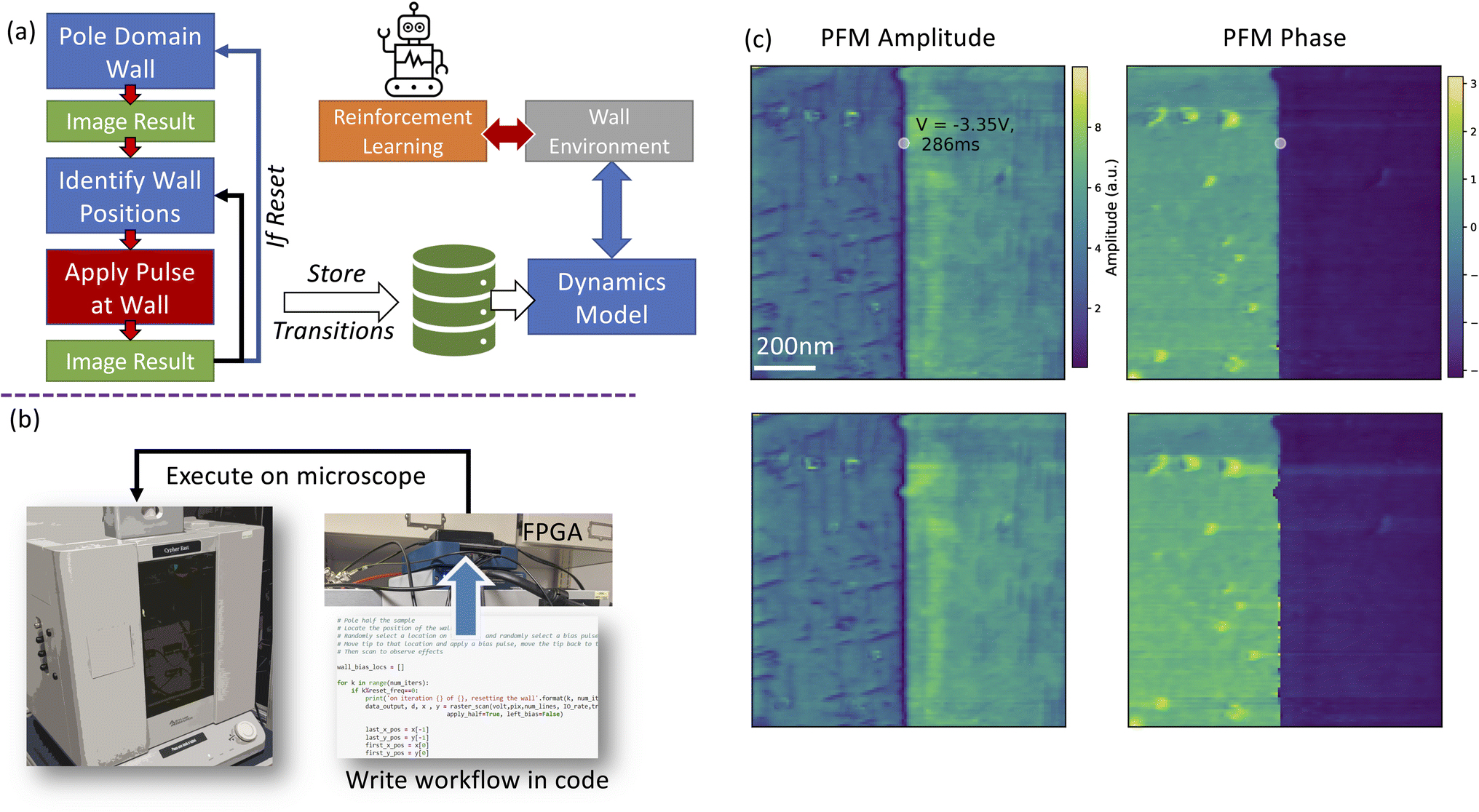 | ||
| Fig. 2 (a) Overall workflow combining experiments with computation. The images (from which states are derived) are in green; actions are in red. (b) A Jupyter notebook with code cells is used to communicate to a home-built program running on an FPGA, that an enables instrument control with fast inputs and outputs for automated experiments. (c) Example vertical PFM amplitude (left) and phase (right) image collected with this workflow, with the original image above and the bias details and location indicated by the white circle. After applying the bias pulse, the sample is reimaged, and clearly shows a displaced domain wall at the location of pulsing (lower panel). | ||
This experimental procedure is coded with python into a Jupyter notebook, which communicates to an FPGA device (Fig. 2(b)) that then executes the workflow steps on the microscope. Details of the FPGA device operation are provided elsewhere,44 but essentially, this acts as an alternate controller for the microscope enabling customized scan paths and excitations to be applied and controlled via python scripts. An example of the initial image, the bias pulse location and parameters, and the result of the bias pulse, are shown in Fig. 2(c). It is observed that applying voltages above a certain threshold produces wall displacements, as expected. The full dataset and a video showing all captured transitions is provided in the ESI S2.† For simplicity, we probe only the vertical PFM signal. Note also that numerous ‘needle’ domains can be seen in the vicinity of the written wall. Some of the data was captured using single frequency PFM, whereas other data were captured with band-excitation PFM measurements, utilizing 1 VAC excitations in both cases. For the BE-PFM measurements, a frequency band of 333 kHz to 413 kHz was utilized.
Dynamics model
Our experiment provided us with 801 useable transitions, i.e., circumstances where the imaging quality was sufficient for use. We developed a dynamics model to predict the displacement of domain walls structures when bias pulses are applied via PFM. The architecture of the dynamics (‘surrogate’) model is provided in ESI S3.† As described above, PFM is used to generate training data for the model that contains sequences of images, and their corresponding actions. Each image is represented by a 128 × 128 pixel array from which a 128-pixel length 1-D domain wall vector St is extracted. Actions are given by three continuous normalized values that correspond to bias location, voltage, and pulse width in that order. Since the wall displacement mostly occurs in the section of the wall around where the bias was applied, the dynamics model only predicts displacements for the wall in these local regions. Therefore, the first action value (the one that corresponds to the location of the bias pulse) is thus used to index the local region of the domain wall. Around the location bias is applied, a local region of the wall is extracted as a 14-pixel length vector, represented by St′. The inputs to the surrogate model are the local region St′ as well as the voltage and pulse width applied. Using these inputs, a neural network with two branches works to predict the displacement for the domain wall in the local region. The first branch takes the domain wall configuration, i.e., St′, while the second branch takes the bias amplitude and pulse width as inputs, and both contain only dense layers. These branches are subsequently concatenated before being passed through two more dense layers to obtain the output. The predicted displacements in local region St+1′ can then be added to the original entire wall structure to generate St+1. Because images are also captured immediately following when the bias is applied, our model's predicted domain wall structures can be compared to the actual, observed domain wall structures. This allows the dynamics model to be trained through a supervised learning method, with a traditional loss function such as mean squared error (MSE).Physics-based loss functions
Due to the limited data available, we found it was necessary to introduce two additional regularizations into the loss function to prevent over-fitting and retain reasonable predictions in accordance with known or postulated physics of the system. We introduced two additional regularizers to the loss function for the dynamics model. The first additional term we add to the loss function is a term that emphasizes the agreement of the prediction with known local physics. In this experiment, the direction of displacement for the domain wall should align with the sign of the voltage for the bias that was applied. When this is not the case and the surrogate model's predictions do not agree with this physical prior, such predictions should be penalized. Therefore, for any pixels in St+1′ whose direction of displacement is opposite the sign (±) for the magnitude of the voltage amplitude applied, a penalty coefficient is multiplied to the difference between the observed and predicted wall locations. The mean-squared-error of St+1′ is then calculated using this penalty to determine the total loss for St+1′ which our dynamics model then attempts to minimize in its displacement predictions. This physics loss appears to be a reasonable constraint to add to the model, as it agrees with not only expectations for this prototypical ferroelectric system, but also simply that it comports with the experimental data (e.g., see the videos in the ESI†). But, it should also be noted that in e.g., the boracite system, domain wall motion counter to the direction of the applied electric field has observed45 and in such circumstances this regularization would be actively detrimental.Additionally, we add an additional ‘global’ physics loss which is based on the expectation that the magnitude of displacement of the surrogate model should be monotonic for both the bias voltage and pulse width values. It should be noted that the increased displacement with increased voltage is consistently observed in the raw data. However, the same was not true for pulse width, potentially due to changes in tip condition or other exogeneous variables. Moreover, we also note that the application of the voltage could cause changes to the underlying defect structure, such as by injecting or redistributing oxygen vacancies or other mobile ions,46 or creating other types of defects (for example, see work by Evans et al.47). We do not rule out this possibility, but we can control the degree to which we enforce this inductive bias by adjusting the strength of this term in the final loss function if desired.
To account for this global physics loss, we implement an additional term into the loss function that acts to promote the monotonicity of the dynamics model with respect to pulse width. During training, for each transition, we sample across the action space of pulse widths to make additional predictions. We then compare the predicted area displaced for each pulse width and add a penalty when the area does not either remain constant or increase for longer pulse widths i.e., when monotonicity is not observed. This loss function acts as a regularization term to help ensure that known physical trends are implemented into the dynamics (surrogate) model. In total, the loss function can be written as

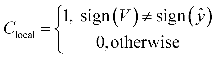
where y is the actual domain wall position, ŷ is the predicted position, and s is the training step number.
The surrogate model is trained with the Adam optimizer for 3000 epochs, and we use an 80/20 training/test split with random splitting of the data. Results after training of the predictions of the model along with real wall displacements are shown in ESI S4.† On the test data, the mean absolute error of the predictions is ∼13.2 nm.
Phase-field simulation results
To better verify our dynamics model, we turned to phase field simulations of the PTO structure. We performed phase-field simulation to further understand the dependence of wall displacement on the applied voltage pulse amplitude and pulse width in (![[1 with combining macron]](https://www.rsc.org/images/entities/char_0031_0304.gif) 0) oriented PTO thin film. Details of the simulations can be found in ESI S5.† As explained earlier we use the transformed coordinate system from hereon for simplicity. All the polarizations in the phase-field result hereafter refer to the global coordinate system. First, the equilibrium domain structure of PTO thin film is generated, which consists of two domain stripes of [−100] and [011] separated by 90° domain walls (Fig. S6†). Next, a positive AFM tip voltage is applied at a pre-existing flat 90° domain wall on the surface of PTO film, while the bottom film is grounded. This causes a large bulge in the domain wall (Fig. 3(a)). The local domain wall displacement (along y) is calculated from the original flat domain wall, which varies along the original flat wall (along x) (see Fig. S7b†). It is clearly seen that the maximum displacement increases with increasing pulse voltage (0.65 V ∼3.26 V) at fixed pulse width (1.15 μs) (see Fig. 3(a)), and with increasing pulse width (0.45 μs ∼2.32 μs) at fixed pulse amplitude (3.26 V) (see Fig. S7a†). Once the domain wall displacement reaches steady state, we moved the tip location to the displaced wall (i.e., the one created with 3.26 V/1.15 μs), and further applied both positive and negative pulse voltages with different amplitudes at fixed pulse width (2.3 μs). Under positive tip voltage, the bulge becomes wider and its width even exceeds the [−100] domain stripes (Fig. 3(e)). The domain wall displacement increases with increasing tip voltage and reaches 16 nm at 3.25 V (Fig. 3(d)). Under negative tip voltage, the original bulge disappears, and a new bulge appears on the other side of the domain stripe (Fig. 3(g and h)), which displaces the domain wall in the opposite direction. The variations of wall displacement with increasing negative voltage (in absolute value) is much smaller than with positive voltage (Fig. 3(g)), and the maximum displacement is calculated to be around −2 nm under −3.25 V. This suggests that depressing the wall (back to an original flat configuration) requires little bias, but pushing it further in the opposite direction requires substantially more. We note here that the phase field simulations show many different domain variants as indicated by the colors in the image. However, we do not see such complicated patterns in the real experiment with PFM. We suggest a reason for this is the underlying simulations code is quite sensitive to local changes in structure. Given that we do not observe evidence of this in the PFM data, we suggest this is likely an artefact. Regardless, these are ignored for the sake of the wall displacement calculations as we simply take the maximum extent of the switched domain regardless of the variant predicted.
0) oriented PTO thin film. Details of the simulations can be found in ESI S5.† As explained earlier we use the transformed coordinate system from hereon for simplicity. All the polarizations in the phase-field result hereafter refer to the global coordinate system. First, the equilibrium domain structure of PTO thin film is generated, which consists of two domain stripes of [−100] and [011] separated by 90° domain walls (Fig. S6†). Next, a positive AFM tip voltage is applied at a pre-existing flat 90° domain wall on the surface of PTO film, while the bottom film is grounded. This causes a large bulge in the domain wall (Fig. 3(a)). The local domain wall displacement (along y) is calculated from the original flat domain wall, which varies along the original flat wall (along x) (see Fig. S7b†). It is clearly seen that the maximum displacement increases with increasing pulse voltage (0.65 V ∼3.26 V) at fixed pulse width (1.15 μs) (see Fig. 3(a)), and with increasing pulse width (0.45 μs ∼2.32 μs) at fixed pulse amplitude (3.26 V) (see Fig. S7a†). Once the domain wall displacement reaches steady state, we moved the tip location to the displaced wall (i.e., the one created with 3.26 V/1.15 μs), and further applied both positive and negative pulse voltages with different amplitudes at fixed pulse width (2.3 μs). Under positive tip voltage, the bulge becomes wider and its width even exceeds the [−100] domain stripes (Fig. 3(e)). The domain wall displacement increases with increasing tip voltage and reaches 16 nm at 3.25 V (Fig. 3(d)). Under negative tip voltage, the original bulge disappears, and a new bulge appears on the other side of the domain stripe (Fig. 3(g and h)), which displaces the domain wall in the opposite direction. The variations of wall displacement with increasing negative voltage (in absolute value) is much smaller than with positive voltage (Fig. 3(g)), and the maximum displacement is calculated to be around −2 nm under −3.25 V. This suggests that depressing the wall (back to an original flat configuration) requires little bias, but pushing it further in the opposite direction requires substantially more. We note here that the phase field simulations show many different domain variants as indicated by the colors in the image. However, we do not see such complicated patterns in the real experiment with PFM. We suggest a reason for this is the underlying simulations code is quite sensitive to local changes in structure. Given that we do not observe evidence of this in the PFM data, we suggest this is likely an artefact. Regardless, these are ignored for the sake of the wall displacement calculations as we simply take the maximum extent of the switched domain regardless of the variant predicted.
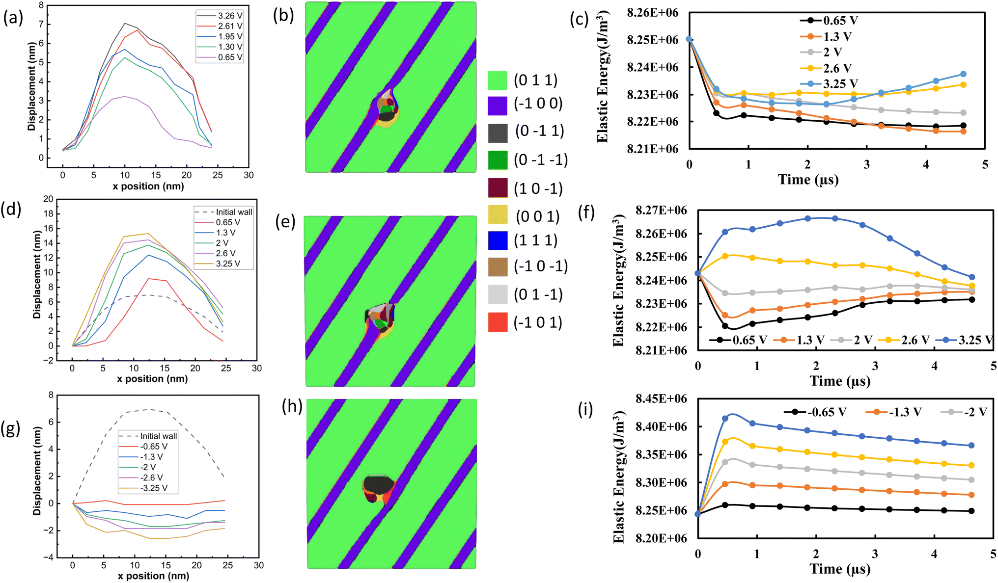 | ||
| Fig. 3 Phase field simulations of a straight and bulged domain wall, after bias application. (a) Predictions of the domain wall profile as a function of voltage, when the tip is placed at an initially flat domain wall and an already bulged wall. The resultant domain wall profiles are shown on the left in (a, d, g) with the (x–y) plane images in (b, e, h) and the elastic energy density is shown on the right, as a function of time in (c, f, i). These simulations are performed for the flat initial wall configuration (a–c), an already ‘bulged’ wall, for positive voltage (d–f) and an already bulged wall for negative bias (g–i). The ‘bulged’ situation is the same one created in (a) where 3.26 V/1.15 μs pulse was applied. Colors in the center panel correspond to different domain variants, as shown in the legend. | ||
Dynamics model predictions
The predictions from our data-driven dynamics model are shown in Fig. 4. In the left column in Fig. 4(a), we show how the wall displaces from an initial flat profile after different bias voltages are applied. Overall, we observe the maximum displacement increasing as the magnitude of voltage and pulse width increases as would be expected. Low voltages also seem to not cause significant displacement, i.e., there is some pinning. The ‘phase diagram’ of the domain wall displacement as a function of the voltages and pulse widths is shown in Fig. 4(b) and indicates (in general) increasing domain wall displacements towards higher voltages and pulse widths as would be expected.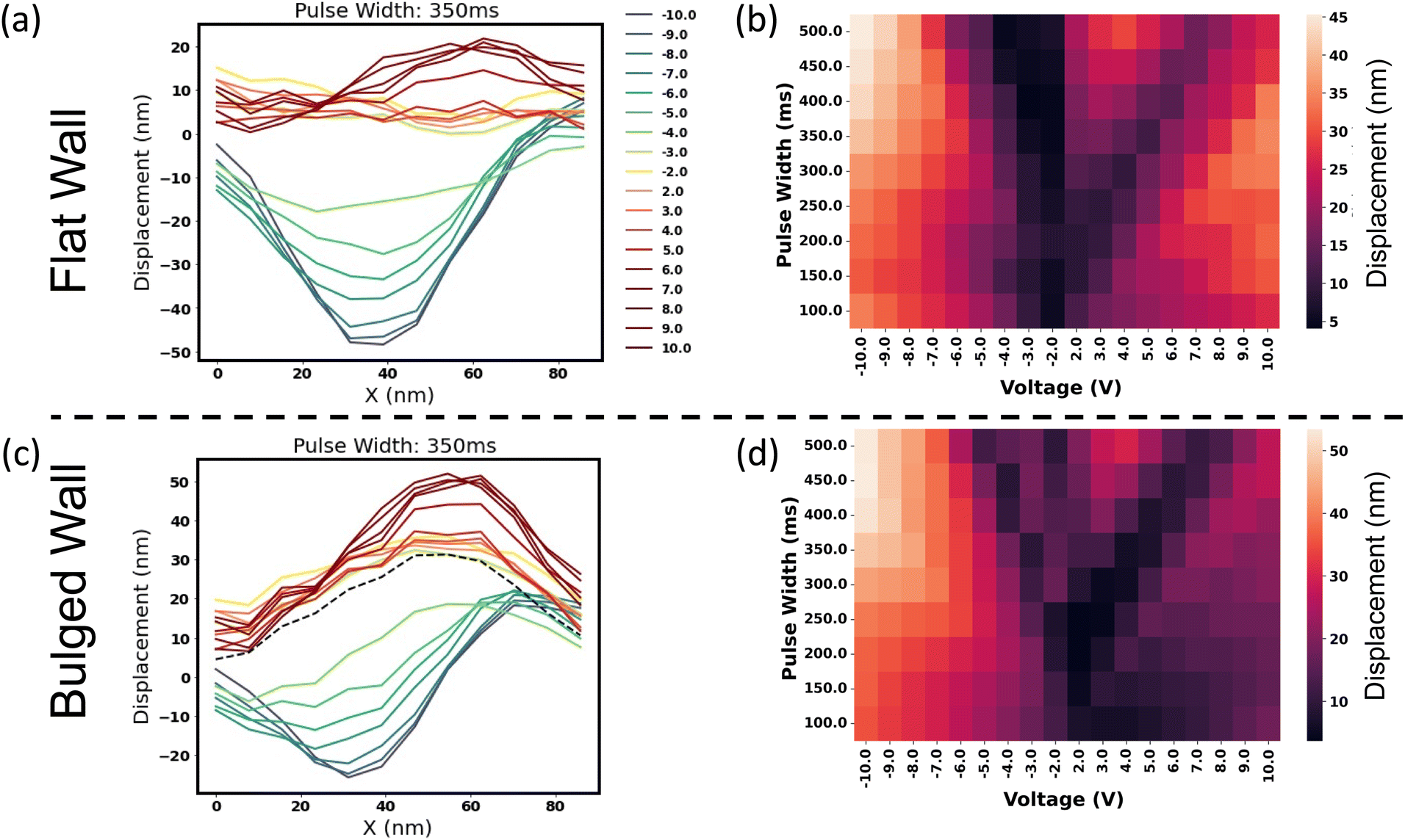 | ||
| Fig. 4 Surrogate model predictions. (a) Predictions of the domain wall profile as a function of voltage, when the tip is placed at an initially flat domain wall, for a fixed pulse width of 350 ms. The maximum displacement map as a function of both variables, assuming a starting flat domain wall profile, is shown in (b). The results for application of bias to an already ‘bulged’ domain wall are shown in (c). In this case the originally bulged wall is created by applying 8 V/300 ms, and the profile it creates is indicated by the dashed line in black. The corresponding displacement map for all voltages and pulse widths for the bulged wall is shown in (d). Note that this map assumes displacements start at 0 for the bulged wall, i.e. it shows the difference from the bulged starting point, not the absolute deviations from the original flat configuration. The color scheme for (a, b) are the same. | ||
However, this diagram clearly still shows some seemingly unphysical behaviors, in particular the dark diagonal that cuts to the top-right of the diagram. One of the reasons for this may be that because we do not consider the surrounding domain structure, and there is limited data, then if a few lower voltage pulses were applied at a domain wall situated next to a strong pinning site (for instance, one of the needle domains), then there would be limited to no motion. The model would fit to these instances and lead to this type of seemingly unphysical result. We attempted to counter this via the addition of physics-based loss regularization, but this is still a ‘soft’ regularization and thus these features could not be eliminated entirely. Alternatively, as mentioned earlier, it is possible that certain defects, e.g. oxygen vacancies, could be injected48 or moved by the application of bias pulses. Such a circumstance would lead to anomalous features on the calculated diagrams based on threshold fields required to initiate such electrochemical processes. We cannot entirely rule out this possibility.
At the same time, the dynamics model allows us to explore the reaction of the domain wall in arbitrary configurations, i.e., to investigate the state dependence. As a simple example, consider the circumstance when the domain wall is already bulged: one would expect a very different response to repeated pulsing in this state, given that the wall configuration is likely already very energetically unfavorable given it will prefer to be flat and reduce elastic energy. This circumstance is modeled in the phase-field simulations in Fig. 3(b) and indicates that when starting with a positive displacement, increasing the positive voltage still does increase the wall displacement in the positive direction, but critically, applying negative bias to this situation very quickly returns the wall to a flat position, even for very low voltages, as seen in Fig. 3(b). That is, there is an asymmetry where returning to a flat profile is more favorable and occurs for lower voltages. This is also seen in the data-driven dynamics model, in Fig. 4(c), and particularly in the ‘phase diagram’ in Fig. 4(d) with brighter colors on the left side of the diagram indicating more propensity to quickly shift the wall to the negative direction, and darker colors on the right indicating resistance to further bulging the wall in the positive direction. These insights suggest that this method can be effectively used to explore the dependence of domain wall dynamics on the existing domain wall configuration, providing another method for domain wall investigations via PFM and automated experiments.
Wall energy and switching dynamics
Next, we explore the use of the surrogate model towards better understanding the domain wall dynamics. We first computed the switched area as a function of bias amplitude and pulse width, for both the flat and bulged wall configurations, and plot them in Fig. 5(a and b). Here it is again clear that for a flat domain wall the switched area does not show strong asymmetry, but for the bulged wall, it is pronounced for the negative side, especially at higher voltages, in agreement with the results form Fig. 4.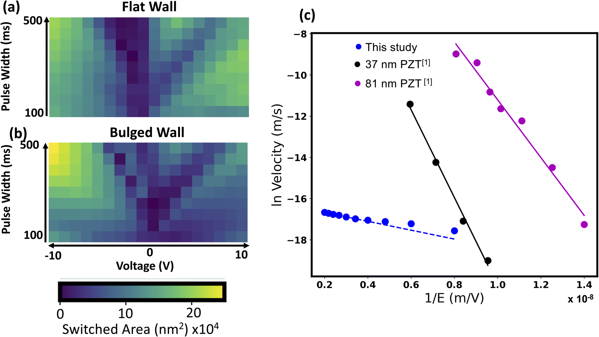 | ||
| Fig. 5 Switching dynamics. (a) Switched areas as a function of voltage and pulse width, for an initial flat wall (a) and a positively bulged wall (b). (c) Velocities of the domain wall calculated for different voltages and 200 ms pulse width (blue) with linear fits in this log vs. 1/E plot shown as a blue dashed line. The linear fit indicates a creep regime. Compared to data by [1] Tybell et al.49 on PZT films in a different geometry, the calculated slope is significantly lower. | ||
To obtain more insight, we calculated the elastic energy density of the domain wall in the different configurations and find there is considerably larger elastic energy at these ferroelastic walls than a typical 180° domain wall in e.g., (001) PZT thin films. We find the energy associated with the wall is about 8.2 × 10⁶ J m−3. For comparison, previous calculations in (001) PZT thin films show that the energy density of a ferroelastic wall in that system is about 2.0 × 10⁶ J m−3, and for a ferroelectric wall, it is about 1 × 10⁶ J m−3.49
The elastic energy densities for the different configurations as a function of bias and time are shown in Fig. 3(c, f and i). When a bias is applied, the elastic energy density as a function of time after the bias is turned on varies in a complex manner depending on the initial state of the wall (straight or bulged) and whether positive or negative polarity is applied. Interestingly, the elastic energy density reduces, for ‘bulging’ when positive bias is applied as shown in Fig. 3(c). When a positive bias is applied to an already bulged wall, the overall elastic energy density does not change significantly, when looking at longer time frames (Fig. 3(f)). Conversely, applying negative potential appears to change the elastic energy density more so. However, the change in elastic energy density for small voltages (e.g., −0.65 V), which is sufficient to erase the ‘bulge’, is negligeable. Given that the elastic energy density does not appear to be significantly greater in the bulged state, we believe that the asymmetry that we observe in the surrogate model can be best explained via a straightforward surface energy argument: since the domain walls are obviously more energetically costly than the surrounding domains, eliminating the bulge will be favorable in most circumstances.
Next, we utilized the surrogate model to obtain estimates for the domain wall velocity in this system, similar to the seminal work by Tybell et al.50 We used the model to predict the domain wall velocities for different voltages assuming a pulse width of 200 ms. For this we assume that the electric field E = V/d, where we assume a value of d = 20 nm. The real electric field is likely to be quite complex in such structures,51 but this estimate serves as a reasonable upper bound. We thus computed the domain wall velocities extracted under this approximation and plot them against those of Tybell et al. for PZT domain growth. Accordingly, we plot the log of the velocity against 1/E in Fig. 5(c). The data fits well to a linear slope, i.e., evidence of a creep regime, however it is very evident that the slope is significantly less than those of ref. 49. Note that the two scenarios are not directly comparable, since in the case of the PZT films the experiments by Tybell et al. were performed with nucleation and growth of domains directly underneath the tip, whereas here we are dealing with extension or contraction of pre-existing domain walls in a different orientation. The slope of the velocity is ∼6.5 times lower than that of (001) PZT films. Although the direct comparison cannot be made, we can conclude that (i) the wall appears to be governed by creep dynamics, and (ii) the mobility is significantly reduced compared to 180° walls in PZT, by two orders of magnitude. Further investigations are required to better understand the nature of the pinning potential in this sample.
Reinforcement learning environment
It is also possible to utilize the learned dynamics model as the basis for a RL environment to train agents to manipulate domain wall structures in silico. Notably, such a scenario would be prohibitively expensive with traditional phase-field methods, given that RL typically requires thousands to millions of state transitions for learning policies on meaningful tasks. Note also that while the surrogate model only acts in a local region, we integrate the model into an environment for the entire domain wall. Using this environment, we can then apply RL to learn policies for how to iteratively apply biases to alter the domain wall towards a target structure. Here we do so in the simulated environment that uses the surrogate model as the model for dynamics.To learn policies to control the domain wall structure, we employed the deep deterministic policy gradient (DDPG) algorithm proposed by Lillicrap et al.,52 and implemented within d3rlpy.53 To show the potential use of RL, we simplify the scenario by reducing the action space to just one action – the pulse width is fixed, and the agent is able to modify only the voltage applied. The position where the pulse is applied is varied linearly in a pre-selected manner, and the agent is able to apply 10 pulses to achieve a domain wall structure close to a pre-determined target structure. The RL policy used is a simple multi-layer perceptron with two layers each with 256 units. The reward given to the agent is the negative of the mean absolute error between the domain wall structure and the targeted structure. As a function of training, the RL agent learns to manipulate the wall structure closer to the target, as shown in the learning curve in Fig. 6(a).
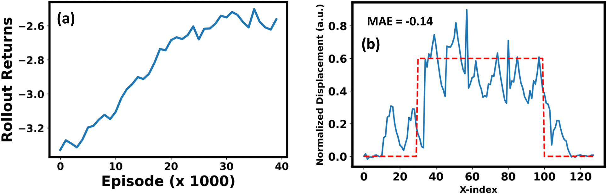 | ||
Fig. 6 Reinforcement learning policy in silico. (a) RL agent returns from the environment as a function of training episode. After 40![[thin space (1/6-em)]](https://www.rsc.org/images/entities/char_2009.gif) 000 episodes the agent's learning saturates. (b) Trial run of trained agent, with the target wall structure plotted as a red dashed line, and the agent's final wall structure created by biasing an initially flat domain wall plotted in blue. The mean absolute error is indicated. 000 episodes the agent's learning saturates. (b) Trial run of trained agent, with the target wall structure plotted as a red dashed line, and the agent's final wall structure created by biasing an initially flat domain wall plotted in blue. The mean absolute error is indicated. | ||
The environment begins with a relatively flat wall and using an RL policy, actions are taken to move the wall towards the target wall structure, indicated by a red dashed line in Fig. 6(b). An example of the resulting domain wall structure after the trained agent has performed actions are shown in Fig. 6(b) (blue line). We observe the agent learns to take actions in regions where the ideal wall is further away from the original wall (i.e., where rewards can increase most significantly). It should again be noted that these are only performed in the simulated environment, not the real experiment. However, training this policy only takes ∼1 hour on a laptop, and even with increasing the action dimensions, it appears possible that it can in future be deployed on operational AFMs.
Discussion
Our work has shown that RL could potentially be used to control PFM to automate the alteration of ferroelectric domain walls. Using PFM image data, we successfully trained a dynamics model to predict the displacement of domain walls for different pulses. Then, with a dynamics model, we were able to train RL agents to learn policies to select action that move the domain wall towards a particular structure. The major advantage of this approach over a traditional human-based workflow is the potential for automatically manipulating structures in a reliable and reproducible manner. Although most SPMs can be programmed to perform tip-based lithography, this requires the bias values to apply to be known ahead of time, and no error correction is possible. In contrast, RL approaches have recently been shown in STM to be useful in precise atomic scale positioning, by Chen et al.54 The RL agent can be continually retrained based on new data and be more adaptable to changing conditions. Perhaps more interestingly, RL agents can be coupled with intrinsic curiosity rewards to enable manipulation and discovery of new types of domain states that are not envisioned by the human operator.There still exist challenges to fully integrate RL automation for domain wall alteration using PFM. Currently, the dynamics model only predicts the 1-D structure of the domain wall. While we can encode information for the areas surrounding the domain wall from PFM images when making predictions, the model itself would have to predict the entire 2-D image for more accurate policies, given the dependence of the actions on the local domain environment. This type of prediction is not feasible due to the limited data currently available. There is a substantial impact of the surrounding domain structure on the underlying dynamics at that position. Given this is a heterogeneous sample, there are many possible domain configurations in the vicinity of a domain wall, and the additional complicating factor of the wall structure itself (for example, bulged or not) will further impact how it responds to electric fields (for instance, see Aravind et al.32). This would require, at minimum, tens of thousands of transitions to be acquired to adequately sample this configurational space, which can only realistically be done through high-throughput scanning methods. This may be possible with methods such as fast scanning via compressive sensing approaches.55
Interestingly, our data was captured on two different instruments (albeit of the same make and model) with different tips on different days, but this did not seem to introduce a level of distribution shift that severely impacted the learning process of the dynamics model. Should this be a problem, one strategy to counter it may be to learn a simple linear model that maps the applied potentials in previous data to applied potentials in the new data that minimizes the discrepancy between the predictions. This is under the assumption that the major tip change will be to affect the applied potential, but not the shape of the domains themselves.
Moreover, ideally one would use the phase-field simulations directly as the physics regularizer, using methods such as structured Gaussian processes, rather than incorporating additional loss terms that are ad hoc defined and may not always be suitable depending on the circumstance. At the same time, the dynamics model learned provides significant insight into the dynamics of domain walls in a state-dependent way that is difficult to recover from more traditional PFM spectroscopic methods, and as such can be convenient for investigating ‘domain wall phase diagrams’. Finally, this approach could be used to optimize for specific properties of the material rather than the specific structure of the domain wall itself, i.e., to solve the inverse design problem of maximizing e.g., photoconductance of domain walls by trialing different wall configurations that maximize the photoconductance reward given to the agent, as opposed to rewarding the generation of a specific structure per se.
Data availability
Python code for reproducing the results in the paper are provided in the included notebooks. The PFM microscopy data is included with the manuscript both as numpy files after processing as well as video files for visualization of the full image data. ESI† is included with this manuscript with more details on the phase field method and the included data files.Author contributions
BRS implemented the dynamics model, trained the RL agent, made figures and co-wrote the paper. RKV designed the study, wrote RL training code, analyzed data and co-wrote the manuscript. YL assisted with experimental measurements. SJ designed the automated acquisition setup. SVK assisted with analysis, interpretation of data and study design. AK assisted with reinforcement learning aspects. BP and YC performed phase field simulations. YCL and JCY grew the sample. All authors commented and edited the manuscript.Conflicts of interest
The authors declare no conflicts of interest.Acknowledgements
The microscopy and reinforcement learning work were supported by Center for Nanophase Materials Sciences (CNMS), which is a US Department of Energy, Office of Science User Facility at Oak Ridge National Laboratory. Y. C. acknowledges the funding support from NSF under the award number NSF 2132105. This work was supported (S. V. K.) by the US Department of Energy, Office of Science, Office of Basic Energy Sciences, as part of the Energy Frontier Research Centers program: CSSAS – The Center for the Science of Synthesis Across Scales – under Award Number DE-SC0019288.References
- D. Meier and S. M. Selbach, Nat. Rev. Mater., 2022, 7, 157–173 CrossRef CAS.
- L. E. C. A. K. Tagantsev and J. Fousek, Domains in Ferroic Crystals and Thin Films, Springer, New York, 2010 Search PubMed.
- N. D. Mermin, Rev. Mod. Phys., 1979, 51, 591 CrossRef CAS.
- T. Yang, V. Gopalan, P. Swart and U. Mohideen, Phys. Rev. Lett., 1999, 82, 4106 CrossRef CAS.
- B. Vul, G. Guro and I. Ivanchik, Ferroelectrics, 1973, 6, 29–31 CrossRef CAS.
- J. Seidel, L. W. Martin, Q. He, Q. Zhan, Y.-H. Chu, A. Rother, M. Hawkridge, P. Maksymovych, P. Yu and M. Gajek, Nat. Mater., 2009, 8, 229–234 CrossRef CAS PubMed.
- A. N. Morozovska, R. K. Vasudevan, P. Maksymovych, S. V. Kalinin and E. A. Eliseev, Phys. Rev. B: Condens. Matter Mater. Phys., 2012, 86, 085315 CrossRef.
- G. Nataf, M. Guennou, J. Gregg, D. Meier, J. Hlinka, E. Salje and J. Kreisel, Nat. Rev. Phys., 2020, 2, 634–648 CrossRef CAS.
- R. K. Vasudevan, W. Wu, J. R. Guest, A. P. Baddorf, A. N. Morozovska, E. A. Eliseev, N. Balke, V. Nagarajan, P. Maksymovych and S. V. Kalinin, Adv. Funct. Mater., 2013, 23, 2592–2616 CrossRef CAS.
- J. Schultheiß, T. Rojac and D. Meier, Adv. Electron. Mater., 2022, 8, 2100996 CrossRef.
- A. Tselev, P. Yu, Y. Cao, L. R. Dedon, L. W. Martin, S. V. Kalinin and P. Maksymovych, Nat. Commun., 2016, 7, 11630 CrossRef CAS PubMed.
- R. Xu, J. Karthik, A. R. Damodaran and L. W. Martin, Nat. Commun., 2014, 5, 3120 CrossRef PubMed.
- F. Xu, S. Trolier-McKinstry, W. Ren, B. Xu, Z.-L. Xie and K. Hemker, J. Appl. Phys., 2001, 89, 1336–1348 CrossRef CAS.
- S. Li, A. Bhalla, R. Newnham and L. Cross, Mater. Lett., 1993, 17, 21–26 CrossRef CAS.
- F. Rubio-Marcos, D. A. Ochoa, A. Del Campo, M. A. García, G. R. Castro, J. F. Fernández and J. E. García, Nat. Photonics, 2018, 12, 29–32 CrossRef CAS.
- F. Rubio-Marcos, A. Del Campo, P. Marchet and J. F. Fernández, Nat. Commun., 2015, 6, 6594 CrossRef CAS PubMed.
- F. Rubio-Marcos, P. Pamies, A. Del Campo, J. Tiana, J. Ordoñez-Pimentel, M. Venet, R. E. Rojas-Hernandez, D. A. Ochoa, J. F. Fernández and J. E. García, Appl. Mater. Today, 2023, 32, 101838 CrossRef.
- N. Balke, S. Choudhury, S. Jesse, M. Huijben, Y. H. Chu, A. P. Baddorf, L.-Q. Chen, R. Ramesh and S. V. Kalinin, Nat. Nanotechnol., 2009, 4, 868–875 CrossRef CAS PubMed.
- J. R. Whyte, R. G. McQuaid, P. Sharma, C. Canalias, J. F. Scott, A. Gruverman and J. M. Gregg, Adv. Mater., 2014, 26, 293–298 CrossRef CAS PubMed.
- G. Catalan, J. Seidel, R. Ramesh and J. F. Scott, Rev. Mod. Phys., 2012, 84, 119 CrossRef CAS.
- C. Ganpule, V. Nagarajan, B. Hill, A. Roytburd, E. Williams, R. Ramesh, S. Alpay, A. Roelofs, R. Waser and L. Eng, J. Appl. Phys., 2002, 91, 1477–1481 CrossRef CAS.
- C. Harnagea, Local piezoelectric response and domain structures in ferroelectric thin films investigated by voltage-modulated force microscopy, Universitäts-und Landesbibliothek, 2001 Search PubMed.
- C. Ganpule, A. Roytburd, V. Nagarajan, B. Hill, S. Ogale, E. Williams, R. Ramesh and J. Scott, Phys. Rev. B: Condens. Matter Mater. Phys., 2001, 65, 014101 CrossRef.
- V. Shvartsman, A. Kholkin, C. Verdier, Z. Yong and D. Lupascu, J. Eur. Ceram. Soc., 2005, 25, 2559–2561 CrossRef CAS.
- R. K. Vasudevan, Y.-C. Chen, H.-H. Tai, N. Balke, P. Wu, S. Bhattacharya, L.-Q. Chen, Y.-H. Chu, I.-N. Lin and S. V. Kalinin, ACS Nano, 2011, 5, 879–887 CrossRef CAS PubMed.
- L. McGilly, P. Yudin, L. Feigl, A. Tagantsev and N. Setter, Nat. Nanotechnol., 2015, 10, 145–150 CrossRef CAS PubMed.
- J. Kim, M. You, K.-E. Kim, K. Chu and C.-H. Yang, npj Quantum Mater., 2019, 4, 29 CrossRef.
- Y. Li, Y. Jin, X. Lu, J.-C. Yang, Y.-H. Chu, F. Huang, J. Zhu and S.-W. Cheong, npj Quantum Mater., 2017, 2, 43 CrossRef.
- Z. Li, H. Shen, G. Dawson, Z. Zhang, Y. Wang, F. Nan, G. Song, G. Li, Y. Wu and H. Liu, J. Mater. Chem. C, 2022, 10, 3071–3080 RSC.
- A. R. Damodaran, J. Clarkson, Z. Hong, H. Liu, A. K. Yadav, C. T. Nelson, S.-L. Hsu, M. McCarter, K.-D. Park and V. Kravtsov, Nat. Mater., 2017, 16, 1003–1009 CrossRef CAS PubMed.
- M. Chen, J. Ma, R.-C. Peng, Q. Zhang, J. Wang, Y. Liang, J. Wu, L.-Q. Chen, J. Ma and C.-W. Nan, Acta Mater., 2019, 175, 324–330 CrossRef CAS.
- V. R. Aravind, A. N. Morozovska, S. Bhattacharyya, D. Lee, S. Jesse, I. Grinberg, Y. Li, S. Choudhury, P. Wu and K. Seal, Phys. Rev. B: Condens. Matter Mater. Phys., 2010, 82, 024111 CrossRef.
- S. Kalinin, B. Rodriguez, S. Jesse, Y. Chu, T. Zhao, R. Ramesh, S. Choudhury, L. Chen, E. Eliseev and A. Morozovska, Proc. Natl. Acad. Sci. U. S. A., 2007, 104, 20204–20209 CrossRef CAS PubMed.
- L. Q. Chen, J. Am. Ceram. Soc., 2008, 91, 1835–1844 CrossRef CAS.
- D. Akbarian, D. E. Yilmaz, Y. Cao, P. Ganesh, I. Dabo, J. Munro, R. Van Ginhoven and A. C. Van Duin, Phys. Chem. Chem. Phys., 2019, 21, 18240–18249 RSC.
- S. Jesse, B. J. Rodriguez, S. Choudhury, A. P. Baddorf, I. Vrejoiu, D. Hesse, M. Alexe, E. A. Eliseev, A. N. Morozovska and J. Zhang, Nat. Mater., 2008, 7, 209–215 CrossRef CAS PubMed.
- B. J. Rodriguez, S. Choudhury, Y. Chu, A. Bhattacharyya, S. Jesse, K. Seal, A. P. Baddorf, R. Ramesh, L. Q. Chen and S. V. Kalinin, Adv. Funct. Mater., 2009, 19, 2053–2063 CrossRef CAS.
- S. V. Kalinin, S. Jesse, B. J. Rodriguez, Y. Chu, R. Ramesh, E. Eliseev and A. Morozovska, Phys. Rev. Lett., 2008, 100, 155703 CrossRef CAS PubMed.
- V. Anbusathaiah, S. Jesse, M. Arredondo, F. Kartawidjaja, O. Ovchinnikov, J. Wang, S. Kalinin and V. Nagarajan, Acta Mater., 2010, 58, 5316–5325 CrossRef CAS.
- G. Lu, S. Li, X. Ding, J. Sun and E. K. Salje, Phys. Rev. Mater., 2019, 3, 114405 CrossRef CAS.
- Y. Ivry, J. F. Scott, E. K. Salje and C. Durkan, Phys. Rev. B: Condens. Matter Mater. Phys., 2012, 86, 205428 CrossRef.
- M. Ziatdinov, Y. Liu, K. Kelley, R. Vasudevan and S. V. Kalinin, ACS Nano, 2022, 16, 13492–13512 CrossRef CAS PubMed.
- D. Alikin, L. Gimadeeva, A. Ankudinov, Q. Hu, V. Y. Shur and A. Kholkin, Appl. Surf. Sci., 2021, 543, 148808 CrossRef CAS.
- Y. Liu, K. Roccapriore, M. Checa, S. M. Valleti, J.-C. Yang, S. Jesse and R. K. Vasudevan, 2023, arXiv, preprint, arXiv:2312.10281.
- J. G. Guy, C. Cochard, P. Aguado-Puente, E. Soergel, R. W. Whatmore, M. Conroy, K. Moore, E. Courtney, A. Harvey and U. Bangert, Adv. Mater., 2021, 33, 2008068 CrossRef CAS PubMed.
- S. V. Kalinin, S. Jesse, A. Tselev, A. P. Baddorf and N. Balke, ACS Nano, 2011, 5, 5683–5691 CrossRef CAS PubMed.
- D. M. Evans, T. S. Holstad, A. B. Mosberg, D. R. Småbråten, P. E. Vullum, A. L. Dadlani, K. Shapovalov, Z. Yan, E. Bourret and D. Gao, Nat. Mater., 2020, 19, 1195–1200 CrossRef CAS PubMed.
- K. P. Kelley, A. N. Morozovska, E. A. Eliseev, V. Sharma, D. E. Yilmaz, A. C. van Duin, P. Ganesh, A. Borisevich, S. Jesse and P. Maksymovych, Adv. Mater., 2022, 34, 2106426 CrossRef CAS PubMed.
- R. K. Vasudevan, M. B. Okatan, C. Duan, Y. Ehara, H. Funakubo, A. Kumar, S. Jesse, L. Q. Chen, S. V. Kalinin and V. Nagarajan, Adv. Funct. Mater., 2013, 23, 81–90 CrossRef CAS.
- T. Tybell, P. Paruch, T. Giamarchi and J.-M. Triscone, Phys. Rev. Lett., 2002, 89, 097601 CrossRef CAS PubMed.
- R. K. Vasudevan, Y. Cao, N. Laanait, A. Ievlev, L. Li, J.-C. Yang, Y.-H. Chu, L.-Q. Chen, S. V. Kalinin and P. Maksymovych, Nat. Commun., 2017, 8, 1318 CrossRef PubMed.
- T. P. Lillicrap, J. J. Hunt, A. Pritzel, N. Heess, T. Erez, Y. Tassa, D. Silver and D. Wierstra, arXiv, 2015, preprint arXiv:1509.02971.
- T. Seno and M. Imai, J. Mach. Learn. Res., 2022, 23, 14205–14224 Search PubMed.
- I.-J. Chen, M. Aapro, A. Kipnis, A. Ilin, P. Liljeroth and A. S. Foster, Nat. Commun., 2022, 13, 7499 CrossRef CAS PubMed.
- K. P. Kelley, M. Ziatdinov, L. Collins, M. A. Susner, R. K. Vasudevan, N. Balke, S. V. Kalinin and S. Jesse, Small, 2020, 16, 2002878 CrossRef CAS PubMed.
Footnote |
| † Electronic supplementary information (ESI) available. See DOI: https://doi.org/10.1039/d3dd00126a |
| This journal is © The Royal Society of Chemistry 2024 |