
 Open Access Article
 This Open Access Article is licensed under a Creative Commons Attribution-Non Commercial 3.0 Unported Licence
Electrochemical exfoliation of 2D materials beyond graphene
Minghao
Zhao
 ,
Cinzia
Casiraghi
* and
Khaled
Parvez
*
,
Cinzia
Casiraghi
* and
Khaled
Parvez
*
Department of Chemistry, University of Manchester, M13 9PL Manchester, UK. E-mail: cinzia.casiraghi@manchester.ac.uk; khaled.parvez@manchester.ac.uk
First published on 16th February 2024
Abstract
After the discovery of graphene in 2004, the field of atomically thin crystals has exploded with the discovery of thousands of 2-dimensional materials (2DMs) with unique electronic and optical properties, by making them very attractive for a broad range of applications, from electronics to energy storage and harvesting, and from sensing to biomedical applications. In order to integrate 2DMs into practical applications, it is crucial to develop mass scalable techniques providing crystals of high quality and in large yield. Electrochemical exfoliation is one of the most promising methods for producing 2DMs, as it enables quick and large-scale production of solution processable nanosheets with a thickness well below 10 layers and lateral size above 1 μm. Originally, this technique was developed for the production of graphene; however, in the last few years, this approach has been successfully extended to other 2DMs, such as transition metal dichalcogenides, black phosphorous, hexagonal boron nitride, MXenes and many other emerging 2D materials. This review first provides an introduction to the fundamentals of electrochemical exfoliation and then it discusses the production of each class of 2DMs, by introducing their properties and giving examples of applications. Finally, a summary and perspective are given to address some of the challenges in this research area.
 Minghao Zhao | Minghao Zhao received his MSc Degree from the Department of Materials Science, at the University of Manchester in 2019. He is currently a PhD student under the supervision of Prof. Cinzia Casiraghi, Department of Chemistry, at the University of Manchester, UK. His research is focused on the electrochemical exfoliation of two-dimensional materials beyond graphene and their integration into printed devices. |
 Cinzia Casiraghi | Prof Cinzia Casiraghi holds a Chair in Nanoscience at the Department of Chemistry, University of Manchester (UK). She received her BSc and MSc in Nuclear Engineering from Politecnico di Milano (Italy) and her PhD in Electrical Engineering from the University of Cambridge (UK). In 2005, she was awarded an Oppenheimer Fellowship, followed by the Humboldt Research Fellowship and the prestigious Kovalevskaja Award (1.5M Euro). In 2010, she joined the Department of Chemistry at the University of Manchester. Her research focuses on 2D material based inks and their use in printed electronics and biomedical applications. She has published more than 100 works in well-respected journals in the field, collecting more than 38 |
 Khaled Parvez | Dr Khaled Parvez received his PhD in chemistry from the Max Planck Institute for Polymer Research, Germany in 2014. From 2014 to 2016, he worked as a post-doctoral fellow in the Carbon Material Innovation Centre at BASF, Germany. In 2016, he joined the research group of Prof. Cinzia Casiraghi at the University of Manchester where he currently works as a Senior Research Associate. His research interests include wet-chemical exfoliation and solution processing of 2D materials, ink formulations, inkjet printing and printed electronics. He has authored and co-authored over 50 peer-reviewed articles. |
1. Introduction
Graphene, a single layer of graphite,1 is the most widely studied 2DM, due to its unique physical, chemical and electronic properties.2–9 However, similar to graphite, there are many layered materials in nature that can be exfoliated into single- and few-layers, providing 2D nanosheets with complementary properties to those of graphene.10–15 The family of 2DMs includes insulators (e.g., hBN and PbS), superconductors (e.g., NbSe2), semiconductors (e.g., transition metal dichalcogenides (TMDs), tellurene, and black phosphorous (BP)), semi-metals (e.g., graphene, WTe2, 1T MoS2, 1T WSe2,…), and metals (MXenes, VO2, VS2, VSe2,…). Furthermore, the surface chemistry of 2DMs can be easily modified by covalent or non-covalent functionalization, hence providing additional properties and functionalities.16,17 Due to the ultra-thin thickness with strong in-plane bonding, 2DMs exhibit excellent mechanical flexibility and high transparency, which are important for their applications in flexible electronics.14,18 Additionally, the high specific surface area of 2DMs makes them very attractive for energy storage,19,20 sensing,21,22 and biomedical applications,23–25 to name a few examples.Furthermore, 2DMs can be easily produced in solution, hence making it possible to use mass scalable and low cost techniques for their processing and integration into devices.26–30 Solution-processed 2DMs can be easily produced by using top-down methods, such as liquid-phase exfoliation (LPE)31 and electrochemical exfoliation (ECE),32–34 or by bottom-up methods, based on wet-chemical approaches, such as colloidal and hydro/solvothermal synthesis, where nanosheets or thin films are produced directly from precursors by chemical reactions under specific conditions (e.g. in the presence of specific ligands and solvents).35–40 The LPE relies on directly exposing the bulk material to a solvent with a favourable surface tension that minimizes the interfacial tension between the solvent and the 2D crystals. This method is typically time consuming and produces nanosheets with large distributions in lateral size and thickness, which strongly depend on the processing conditions,41,42 hence giving rise to possible reproducibility issues, in particular when the method is extended to large scale production. The ECE is based on the expansion of the layers of the bulk material by intercalation of ions and small molecules, followed by separation and dispersion of the nanosheets in a solvent. Amongst these approaches, ECE is one of the most attractive methods to produce solution-processed 2DMs, as the setup is relatively simple to build and operate, exfoliation usually requires just one step and can be performed under ambient conditions. Furthermore, the use of an electric field facilitates ion intercalation and hence the nanosheet separation, often providing good exfoliation efficiency compared to other intercalation-based techniques. Finally, ECE provides higher control over the quality of the products, as compared to other techniques: the lateral size, thickness, defect density, crystal structure and oxygen content can all be tuned by adjusting the exfoliating voltage or current, the type of electrolyte, and so on.43
The research progress on the ECE preparation of 2DMs has significantly advanced in the last decade. The ECE approach has a rich historical background that lies on the scientific foundation of graphite intercalation chemistry.44–47 Graphite intercalated compounds (GICs) are defined as graphite with various amounts of molecular layers intercalated between the constituent graphene sheets. The intercalating molecule can either donate or accept an electron, forming an ionic bond with graphite; it is also possible to have ternary GICs, with both acceptors and donors co-intercalated.48 GICs have attracted considerable research interest as they show different electronic and magnetic properties as compared to pristine graphite.49 In addition, they can be used for various applications, from batteries to highly conductive graphite fibers.46 While GICs have been studied for over a century, it was not until the 1970s and 80s that electrochemical techniques were used to prepare GICs by the intercalation of pure sulfuric acid,50 alkali metal ions,51 metal halides,52 fluoride ions,53,54 magnesium ions55 and lithium ions56 into graphite interlayers. In 1998, Bourelle et al. reported the preparation of expanded graphite by using electrochemical intercalation of sulfuric and formic acid mixtures.57 Later in 2003, Weng et al. reported the electrochemical exfoliation of 40 nm size graphite nanoparticles from a graphite electrode in aqueous ammonia solution.58 However, the research on the exfoliation of GICs to form graphene-related materials intensified only after 2004, with the isolation of graphene.59 In 2009, Wang et al. first used ECE to exfoliate few-layer graphene nanosheets of 1–2 μm lateral size from graphite rods using poly(styrenesulfonate) (PSS) as an electrolyte.60 The exfoliated graphene showed a significant density of defects, such as oxygen functional groups as well as residual PSS molecules. Since then, significant progress has been made on the ECE method to prepare graphene and graphene related materials,61–64 and recently, it has been extended to the preparation of other 2DMs, such as TMDs,65,66 black phosphorous,67–69 post-transition metal chalcogenides (PTMCs) (e.g. In2Se3, Sb2S3, Sb2Te3etc.),70,71 metal phosphorous trichalcogenides (MPTs) (e.g. NiPS3),72–74 2D monoelemental materials (e.g. As, Te, Bi, Ge, Sb etc.),75–77 graphitic carbon nitride,78 transition metal oxides,78 metal organic frameworks (MOF) nanosheets,79 and MXene,80 to name a few examples (Fig. 1). In particular, semiconducting 2DMs produced by ECE have been shown to provide electronic properties good enough to be used as semiconducting channels in transistors.65,81–83 Because of the fast progress in the synthesis of 2DMs by ECE and their potential use in many applications, ranging from electronics to energy storage devices, we describe in this review the results obtained for each 2DM. As the number of 2DMs is very large, we have divided the discussion among different families of 2DMs, so the reader can refer directly to the 2DM of interest.
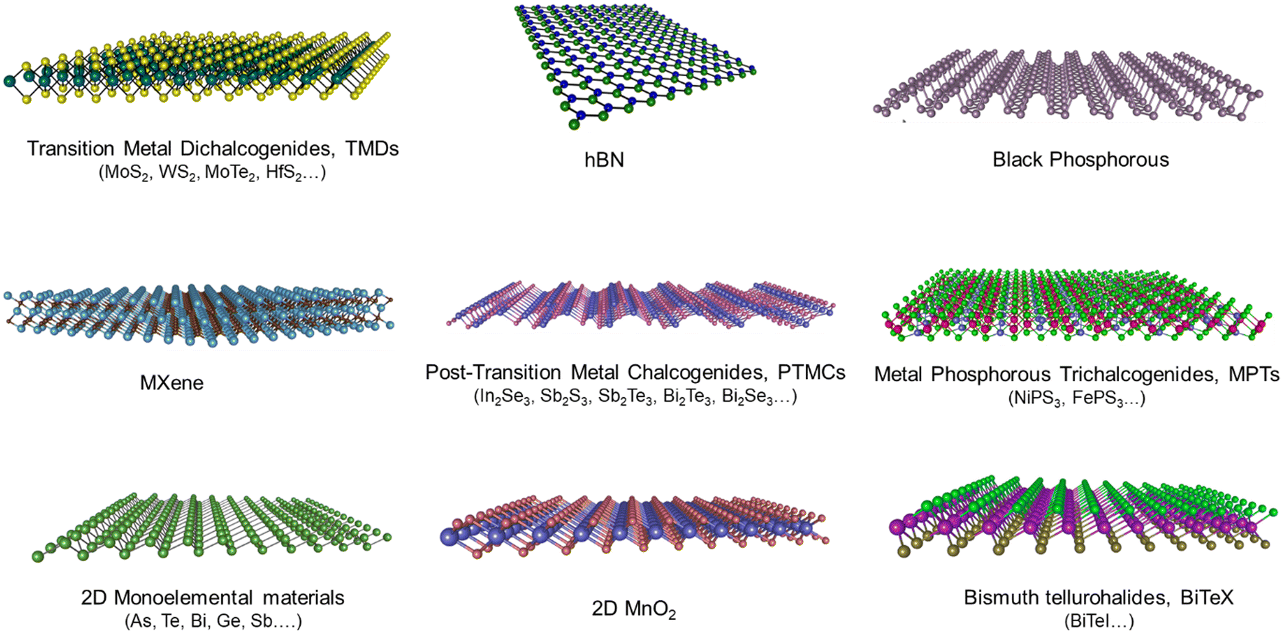 | ||
| Fig. 1 Crystal structures of some of the 2D materials that can be produced by ECE. | ||
This review first introduces the general principle of ECE, based on the exfoliation of graphite, and then provides a comprehensive report on the recent developments in the ECE of emerging 2DMs, focusing mostly on the advances obtained in the last 5 years. Readers who are interested in ECE of graphene only can find more details in previously published reviews.62,64,84–86 Finally, in the last section, we conclude this review by highlighting the advantages and disadvantages of the ECE. Additionally, a perspective on some of the challenges that need to be addressed in this research area is given, with a particular focus on 2DMs beyond graphene.
2. General principle and mechanism
Electrochemical exfoliation is traditionally performed by direct contact of the bulk layered material with the power source. This is done using an electrochemical cell, which is composed of three parts: the electrodes (working electrode, WE, and counter electrode, CE), the liquid electrolyte and the power supply (Fig. 2). Once a suitable voltage is applied between the WE and the CE, depending on the applied potential of the WE, either anions or cations from the electrolyte solution will intercalate between the interlayer spacing of the bulk materials, resulting in structural expansion and leading to the delamination of the bulk 2DM into suspended thin layers.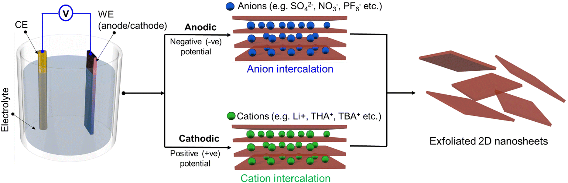 | ||
| Fig. 2 Schematic illustration of a typical electrochemical cell and representative ion intercalations at the anode and the cathode leading towards the exfoliation of 2D nanosheets. | ||
The electrolyte can contain either anions, such as sulfate (SO42−), bisulfate (HSO4−), hydroxide (OH−), perchlorate (ClO4−), trifluoroborate (BF4−), nitrate (NO3−), phosphate (PO43−) and hexafluorophosphate (PF6−) etc., or cations, such as alkali ions (e.g. Li+, K+ and Na+), quaternary ammonium ions (e.g. tetrapropylammonium (TPA+), tetrabutylammonium (TBA+), tetraheptylammonium (THA+))34,87 The CE is made of metallic wires or plates, such as platinum (Pt) foil/wire or glassy carbon electrodes, as they have sufficient stability in the electrochemical environment. The WE is made from the bulk layered material and can be in the shape of a rod, foil, flake or plate. Depending on whether the intercalant is an anion or a cation, the WE could serve as either an anode or a cathode; hence, ECE is classified as either anionic or cationic, respectively (Fig. 2).
Generally, anodic exfoliation is performed in an aqueous electrolyte, while cathodic exfoliation is performed in nonaqueous electrolytes containing organic solvents such as N-methyl-2-pyrrolidone (NMP), propylene carbonate (PC), dimethyl carbonate (DMC), and dimethylformamide (DMF).88–90 Anodic exfoliation always utilises a positive potential to drive the intercalation of anions of the electrolyte (or anions produced in electrolysis reaction) into the anodic working electrode in an aqueous solution.91 Many types of electrochemical anodic exfoliation processes have been proposed for the preparation of graphene from bulk graphite; however, the sulfate (SO42−) ion represents one of the most efficient negative ion intercalants because its ionic size (0.46 nm) is similar to the graphite interlayer spacing (0.33 nm).92 During the electrochemical processes, the ˙OH and ˙O radicals are produced by the reduction of water at the cathode and are co-intercalated with sulfate ions into the bulk graphite followed by the reduction of intercalated sulfate ions; at the same time, self-oxidation of water produces gaseous species such as SO2, O2 and H2 leading to the delamination of graphene nanosheets from the bulk graphite.34,93 Many studies have demonstrated high yield preparation by anodic ECE of thin (1–3 layers) graphene nanosheets with large lateral sizes (typically >5 μm).34,62,93 However, the formation of radicals during the anodic process results in the oxidation of the exfoliated graphene. Nevertheless, the anodic electrochemical process has been used to prepare various types of graphene-based materials, such as graphene oxide, heteroatom doped graphene, nanoparticle/graphene hybrids etc.61,94 The anodic exfoliation strategy has also been used to prepare other 2DMs, such as MoS2, black phosphorus, MXene, borophene etc.66,67,95,96 Although the anodic exfoliation process enables efficient production with high production rates (e.g. producing gram scale quantity within a few minutes to hours in the lab), it results in an unavoidable oxidation of the exfoliated materials due to the radical formation in aqueous media. This can be a major drawback for certain applications, such as in electronics where high quality 2DMs are needed.
On the other hand, the cathodic exfoliation process is a favourable route to produce 2D materials without affecting their intrinsic properties, as it is based on a non-oxidative exfoliation process. Cathodic exfoliation is usually conducted in an organic solution of alkali ions or quaternary ammonium, where a negative potential is applied to the layered material for the intercalation of positively charged ions. The use of organic solvents has the benefit of limiting the oxidation of the nanosheets. In the case of graphene, this method was successfully used to produce thin graphene nanosheets (1–5 layers) with a small degree of oxidation.97,98 However, as compared to anodic exfoliation, the process is extremely slow and generally produces nanosheets of smaller size. Cathodic ECE can also be successfully applied to 2DMs beyond graphene: in 2011, Zeng's group performed cathodic ECE of MoS2 for the first time using Li foil as the anode and LiPF6 (dissolved in a mixture solvent of ethyl carbonate (EC) and DMC) as the electrolyte.99 The negative bias drives the insertion of Li+ into MoS2 layers and weaken the interlayer van der Waals interactions, converting bulk MoS2 into the intercalated compound LixMoS2. The compound is then sonicated in water to produce water based MoS2 dispersions. During sonication, the inserted Li ions react with water to form H2 and further separate the layers. However, it was observed that Li intercalation introduces a large number of extra electrons into the crystal, leading to phase transformation of the semiconducting 2H into the metallic 1T phase. The product mainly contains the metallic 1T phase, hence making it difficult to apply this material in electronics without further processing. Alternative cathodic ECE strategies have been recently developed using the quaternary ammonium salts and/or anodic ECE strategies using inorganic salt-based electrolytes, enabling to retain the semiconducting nature (i.e. the 2H phase) of MoS2, as it will be discussed in detail in Section 3.2.
It is worth noting that during exfoliation, there is a risk of having the WE disintegration before the intercalation is complete. This can severely reduce the yield, lateral size, and thickness as well as the production rate of the exfoliated materials. Hence, a suitable electrode preparation method is essential to prevent its fracturing during the exfoliation. Common strategies to increase mechanical robustness include compressing the bulk material to make a pellet or using a porous support framework (such as platinum gauze or mesh, carbon cloth or plastic tube) to wrap the electrode.71,100,101 These strategies ensure continuous electrical contact of the 2D crystals throughout the exfoliation process. In addition, a large number of layered bulk materials beyond graphite are not conductive, hence, a large applied potential is required to overcome their high resistance. In such cases, the inclusion of a conducting additive is an effective strategy to improve the WE conductivity, by enabling to perform ECE of a wide range of non-conductive materials and by using relatively small potentials.91,101 Moreover, the thickness and lateral size of the exfoliated nanosheets largely depend on the size of the anionic and/or cationic intercalating ions, their concentration in the electrolyte, the applied potential as well as the interlayer spacing of the bulk crystals. Typically, thin and large 2D nanosheets are obtained when large and single crystalline bulk material is used as precursor, whereas the use of powder-type bulk material results in a smaller size of the exfoliated nanosheets.102
The ECE is traditionally performed by direct electrical contact between the bulk crystal and the power source. This sets some restrictions on the shape and size of the starting bulk material. For example, it is extremely difficult to apply ECE to starting bulk material in the form of small flakes or powder.103 A non-contact ECE approach, referred to as “bipolar exfoliation” (BPE) has been proposed to overcome this problem.104,105 The bipolar exfoliation method is inspired by the concept of bipolar electrochemistry, which is a phenomenon based on the polarisation of conducting objects in a DC electric field.106
A typical bipolar exfoliation cell has a similar structure as the cell used in traditional ECE, differing only in the electrode structure, as shown in Fig. 3(a): the bipolar exfoliation cell contains three electrodes, including two feeder electrodes (FE) and a bipolar electrode (BE). During the exfoliation, a uniform electric field is generated across the solution and between the FE electrodes leading to asymmetric polarizations (δ+, δ−) at the edges of the conductive BE without having direct contact with the FE electrodes. Thus, depending on the distance between the FE electrodes and the applied electric field, a potential difference is produced within the BE electrode material in solution. The potential difference drives redox reactions at the edges of the BE material in solution (Fig. 3(b)). Therefore, if the difference in applied potential is large enough to initiate water splitting reactions with the accompanying gas release (H2 and O2 at the cathode and the anode, respectively), this will result in mechanical disintegration of the material over an extended time period.104 Since BPE relies on the faradaic reactions at the two poles of an object polarized in an electric field, it works very well on elongated nanomaterials, such as nanotubes.107 Unlike anodic and/or cathodic exfoliations, the BPE enables to use materials in the form of powders, flakes and particles as BE. However, the BPE usually produces thick nanosheets and it is time consuming, compared to anodic and/or cathodic exfoliations. Moreover, due to the redox reactions that occur during the BPE process, the exfoliated material suffers from oxidation. Nevertheless, this method has been recently applied to the exfoliation of various 2DMs, such as graphene,103 black phosphorus,108 tungsten disulfide,109 and hBN.110 More details are given in Section 3.
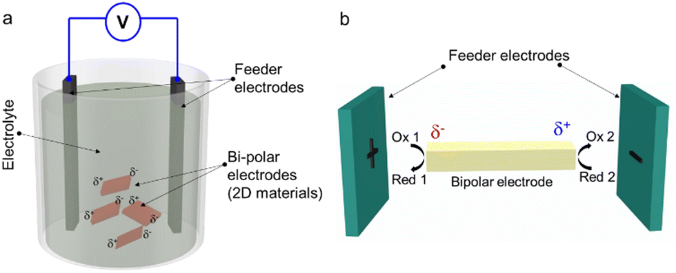 | ||
| Fig. 3 (a) Schematic illustration of a standard bipolar exfoliation cell. (b) Schematic illustration of bipolar electrochemistry, showing the behaviour of conducting species immersed in an electrolytic solution, containing the electroactive red 1 and ox 2 species, exposed to a sufficiently high electric field. | ||
3. State of art
3.1 Hexagonal boron nitride
Single-layer hexagonal boron nitride, also known as ‘white graphene’, is an isoelectronic analogue of graphene, consisting of an equal number of boron and nitrogen atoms covalently bonded by sp2 hybridisation, and has attracted significant research interest for applications in transistors, sensors, and optoelectronics, due to its unique properties.111 This 2DM is an insulator with a bandgap of ∼5.97 eV, showing an atomically flat surface without dangling bonds and only a 1.7% lattice constant mismatch with graphene.112 Additionally, it has excellent thermal stability (reaching 1000 °C in air, 1400 °C in vacuum) and thermal conductivity(∼484 W m−1 K−1) and has strong resistance to oxidation and corrosion.113,114 Therefore, single- and few-layers h-BN are often used in 2DM-based heterostructures, for example as a gate dielectric or a capping layer.115–117The ECE of h-BN was first achieved by the Zeng group, based on highly controlled lithium intercalation, in 2012.118 In the process, the bulk material was first mixed with poly(vinylidene fluoride) (PVDF) binder and acetylene black in a ratio of 80![[thin space (1/6-em)]](https://www.rsc.org/images/entities/char_2009.gif) :10:10 in N-methyl pyrrolidone (NMP). Then, the formed slurry was coated on Cu foil and vacuum dried to fabricate the cathode in the ECE cell. A lithium foil was selected as the anode, and 1 M LiPF6 was added to a mixture of DMC and EC (v/v = 1:1), which was used as electrolyte. The intercalation was achieved by applying a current of 0.025 mA. Finally, delamination was completed by sonicating the rinsed and dried anode in water for 10 min. Characterization indicates the presence of few-layers h-BN, with typical thickness of 2–8 nm and lateral dimension of up to 730 nm.
:10:10 in N-methyl pyrrolidone (NMP). Then, the formed slurry was coated on Cu foil and vacuum dried to fabricate the cathode in the ECE cell. A lithium foil was selected as the anode, and 1 M LiPF6 was added to a mixture of DMC and EC (v/v = 1:1), which was used as electrolyte. The intercalation was achieved by applying a current of 0.025 mA. Finally, delamination was completed by sonicating the rinsed and dried anode in water for 10 min. Characterization indicates the presence of few-layers h-BN, with typical thickness of 2–8 nm and lateral dimension of up to 730 nm.
Even though lithium intercalation provides an efficient way to produce high-quality h-BN nanosheets, the complicated electrode fabrication process is not suitable for large-scale production. In recent years, Wang et al. proposed a low-cost BPE approach (Fig. 4(a)):110 the cell consists of two platinum electrodes as FE and an aqueous electrolyte (containing 0.5 M sodium sulfate and 0.5 mg mL−1 well-dispersed bulk h-BN particles), as shown in Fig. 4(b)–(d). The purpose of adding sodium sulfate is to act as a supporting electrolyte, enhancing the current through the h-BN dispersion. The concentration was optimised so that the increased current would lead to efficient exfoliation without damaging the structure of h-BN. The exfoliation was achieved by applying 10 V to the cell for 30 min. Exfoliation was attributed to the polarisation of the bulk h-BN particles by the field between the two feed electrodes. The electrochemical reactions, such as the electrolysis of water, were promoted at the polarised extremities of the bulk h-BN particles, even in the absence of direct ohmic contact.109,110,119 Final products have an average lateral flake size of 1.27 μm ± 0.48 μm with an average thickness of 8.4 nm ± 3.3 nm (Fig. 4(e)–(g)). X-ray Photoelectron Spectroscopy (XPS) revealed that the bipolar exfoliated hBN nanosheets have a high degree of crystallinity and are free of oxidation (Fig. 4(h)–(j)). This work demonstrated the applicability of BPE to insulators, which had been assumed to be impossible in the early days.
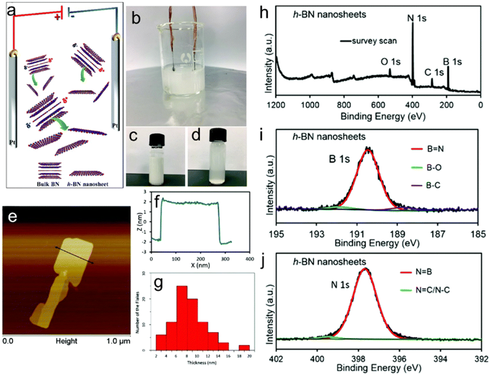 | ||
| Fig. 4 (a) Schematic illustration and (b) picture of the setup used to conduct bipolar electrochemical exfoliation of bulk h-BN. (c) Pristine h-BN dispersion and (d) h-BN nanosheet suspension obtained from exfoliation. (e) AFM image and (f) corresponding height profile of an exfoliated h-BN nanosheet. (g) Statistical analysis of the thickness distribution of the exfoliated hBN. (h) XPS survey spectra of the h-BN nanosheets. High resolution XPS spectra of (i) B 1s and (j) N 1s regions of the h-BN nanosheets, respectively. Reproduced with permission.110 Copyright 2018, RSC Publishing. | ||
3.2 Transition metal dichalcogenides
TMDs show great potential in electronics, optoelectronics, catalysis, energy conversion and storage applications.120–123 Generally, TMDs exhibit an MX2 stoichiometry, where M represents transition-metal (Mo, W, V, etc.) and X stands for chalcogen (S, Se and Te).124–126 Depending on their specific chemical composition, TMDs exhibit different electronic behaviour, from semiconductors to superconductors. For example, single-layer MoS2 and WS2 are direct-band gap semiconductors, while WTe2 and TiSe2 are semimetals, and NbSe2 and TaS2 reveal superconductivity at low temperatures (∼0.8 K).127–130 TMDs exist in 2H, 1T and 3R polymorphs, associated with hexagonal, trigonal and rhombohedral structures, respectively. While the 2H and 3R phases are semiconducting, the 1T phase is metallic. In general, a TMD can be found in multiple polymorphs, depending on how the material is produced. For example, natural MoS2 is commonly found in the 2H phase, whereas synthetic MoS2 often contains the 3R phase.131 On the other hand, 1T MoS2 does not exist in nature, thus it is generally prepared by thermal annealing or by lithium ion intercalation of the 2H phase. TMDs in 1T phase are 107 times more electrically conductive than the corresponding material in 2H phase. Furthermore, TMDs in 1T phase have additional reaction sites and thus are superior to the 2H phase for applications such as catalysis and energy storage, because the charge transfer resistance is dramatically reduced in the metallic phase.132–134 However, one of the most attractive applications of TMDs is in electronics and opto-electronics, where the 2H phase is required. In particular, these types of 2DMs are strongly needed for the next generation field effect transistors (FETs) because they can provide improved device functionalities, such as high sensitivity, flexibility, and low weight as well as low fabrication costs and simple integration onto flexible substrates.135–139 However, the properties of semiconducting nanosheets provided by conventional exfoliation methods (e.g., LPE) are currently not good enough to compete with other solution-processed semiconductor materials used for transistors (e.g., carbon nanotubes).140–142 This may be due to a combination of different factors, such as the relatively small size of the flakes produced by LPE as well as the introduction of defects during exfoliation. Therefore, it is of crucial importance to develop alternative techniques for the production of semiconducting 2DMs of high electronic quality.In 2011, Zeng et al. reported the cathodic exfoliation of various TMDs with a battery-type electrochemical cell, used to intercalate lithium ions into bulk TMDs by using 1.0 M LiPF6 in an electrolyte consisting of 1:1 volume ratio mixture of EC and DMC.99 The fully Li+ ion intercalated TMD layers were separated by treatment with water, by exploiting in situ H2 gas formation between the layers, which further pushed the layers apart. Compared to traditional diffusion kinetics, electrically driven-Li ion intercalation can be controlled through discharge curves and therefore is more efficient. Recently, the same research group presented a modified approach for high-yield production of mono- and few-layer TMDs via electrochemical lithium intercalation.143 As shown in Fig. 5(a), the exfoliation was achieved in a coin type cell using uniformly coated bulk TMD material on a copper (Cu) foil as a cathode and a Li foil as an anode, a polypropylene film based separator, and an electrolyte containing 1.0 M LiPF6 in a mixture of EC and DMC (1:1 volume ratio). Depending on the type of TMDs, a material dependent galvanostatic discharge current of 0.05–0.025 mA and a cut-off voltage of 0.1–0.9 V were applied to complete the intercalation. The intercalation was highly controlled through the discharge curves to achieve sufficient insertion, while avoiding material decomposition. After intercalation, the TMDs were treated with DI water causing the intercalated Li ions to react with water to form lithium hydroxide (LiOH), along with the release of H2 gas, which expands the interlayer distance and weakens the van der Waals interactions between the layers, thus helping separation of the nanosheets. The synthesis of ten types of 2DMs, including MoS2,WS2, TiS2, TaS2, graphene, h-BN, NbSe2, WSe2, Sb2Se3 and Bi2Te3, was achieved (Fig. 5(b)). Subsequent characterisation confirmed the high crystallinity, while a yield of monolayer nanosheets over 90% was achieved (Fig. 5(c)–(h)). Compared with the conventional chemical Li-ion intercalation, this method was performed under milder conditions with a higher degree of quality control. However, constructing a coin type battery cell is complicated and the lithiation process usually takes several days. In addition, it requires the use of metallic Li foil, which can be dangerous and thus limits its practical application. To overcome these problems, in 2017 Ejigu et al. achieved scalable and reproducible cathodic exfoliation of the metallic (1T) phase MoS2 by applying −4.5 V in 0.1 M LiClO4 in a DMC and EC mixture under an N2 atmosphere for 2 h.102 Both Raman and XPS spectra revealed that the exfoliated MoS2 nanosheets have 1T phase. Statistical analysis by AFM showed that the average lateral size was between 300 and 500 nm, with the majority of the flakes (>95%) being 4.5 nm thick. The phase changes from 2H to 1T are attributed to the donation of electrons from the Li+ ion into the MoS2 conduction band: upon intercalation, electron transfer from Li to the unoccupied 4d orbitals takes place effortlessly, resulting in the production of the metallic MoS2 structure. It has been suggested that the content of Li in the intercalated MoS2 crystal determines the most favourable phase of MoS2. For example, the intercalation proceeds without disrupting the 2H phase when x ≤ 0.1 in the LixMoS2 structure. However, as the concentration of Li surpasses the threshold (i.e., x ≥ 0.1), the octahedral 1T phase becomes more stable. Nevertheless, the exfoliated 1T MoS2 showed excellent catalytic performance towards hydrogen evolution reaction and as electrode in supercapacitors.102 Similarly, in 2018, Garah et al. achieved scalable exfoliation of MoS2 in an electrolyte solution containing LiCl in dimethyl sulfoxide (DMSO).144 The exfoliated materials consist of 1–3 layers with 60% of the nanosheets being semiconducting (i.e., having the 2H phase). Although the electrochemical Li-ion intercalation is more controllable than the chemical intercalation, the toxicity, high cost as well as flammability of Li compounds under ambient conditions limit the widespread use of this approach. In 2021, Yu et al. reported a highly efficient cathodic exfoliation of 1T′ MoTe2 without using Li based electrolytes. It has been reported that TMDs become highly unstable when reduced to the thickness of a monolayer due to oxidation in air. This is the case of MoTe2, which then assume a Peierls distorted 1T phase (named 1T′). Thin 1T′ MoTe2 nanosheets were directly exfoliated from bulk crystals using a mixed electrolyte containing tetrahexylammonium chloride (THACl) in PC and polyvinylpyrrolidone (PVP) dissolved in DMF (Fig. 5(i)).145 It was observed that the presence of PVP in the electrolyte not only facilitates the exfoliation process, but also improves the dispersion of the exfoliated flakes by avoiding irreversible stacking of the dried nanosheets, hence making the material stable in various solvents (Fig. 5(j)). This exfoliation strategy resulted in high yield (>95%) of pristine monolayer 1T′ MoTe2 with average lateral sizes of 5–10 μm (Fig. 5(k) and (l)). In addition, the process was used to exfoliate all the group IV semiconducting TMDs. Finally, the exfoliated 1T′ MoTe2 flakes were used as a saturable absorber, showing a stable generation of ultrashort pulses (<150 fs) from mode-locked lasers.
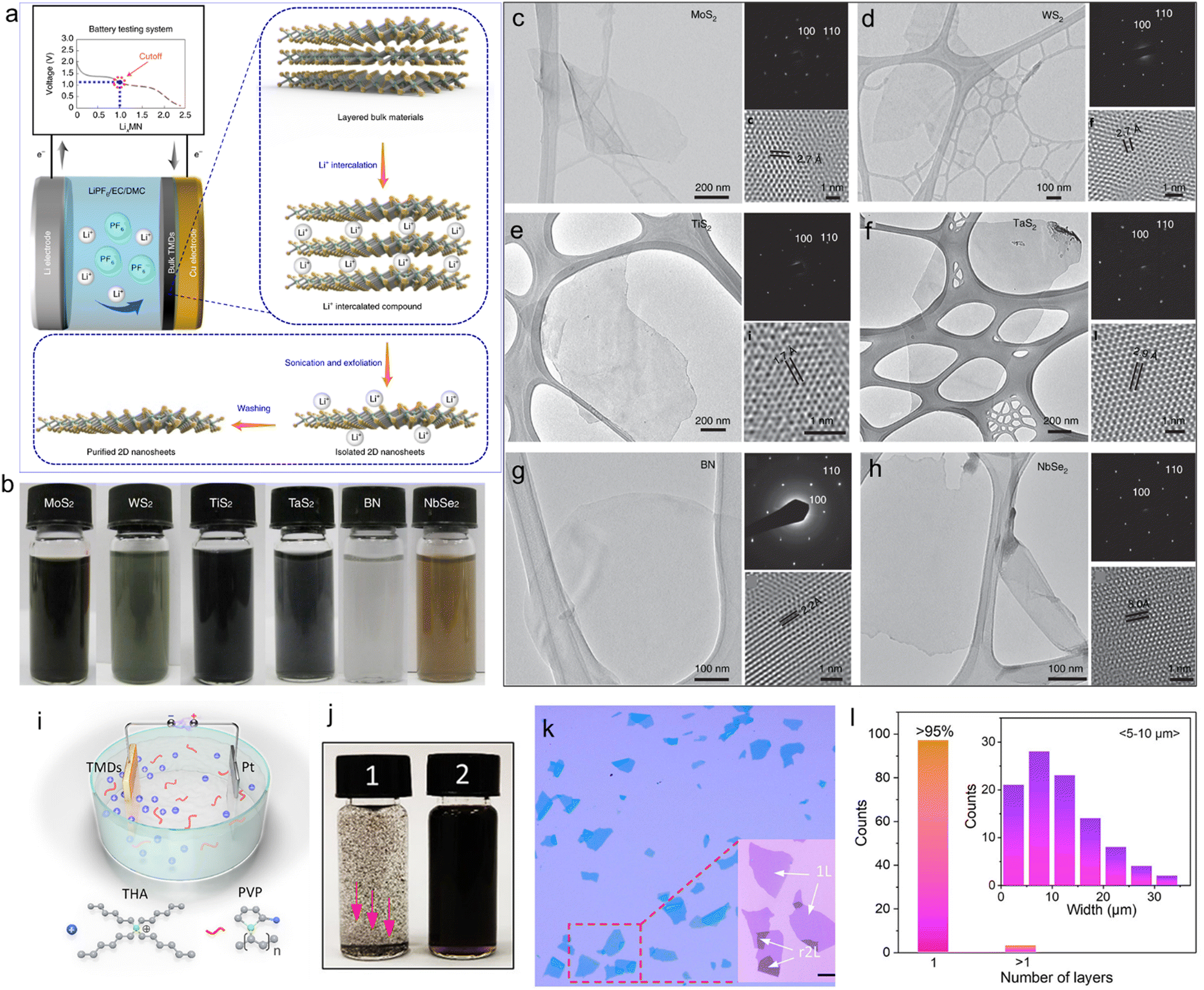 | ||
| Fig. 5 (a) Schematic illustration of the electrochemical lithium intercalation-based exfoliation process. (b) Picture of the dispersions of various exfoliated TMDs. Transmission Electron Microscopy (TEM) images with corresponding SAED patterns and HRTEM images of exfoliated: (c) MoS2, (d) WS2, (e) TiS2, (f) TaS2, (g) BN and (h) NbSe2, respectively. Reproduced with permission.143 Copyright 2022, Springer Nature. (i) Schematic illustration of the electrochemical exfoliation setup using THA as an intercalant and PVP as a surfactant. (j) Photos of the exfoliated 1T′-MoTe2 solution without (1)/with (2) PVP, after manual shaking. Red arrows in (1) indicate the precipitation of the exfoliated flakes. (k) Optical microscopy images of PVP-assisted exfoliated 1T′-MoTe2 flakes, showing the same optical contrast for all the flakes. r2L refers to the restacked bilayer. (l) Statistical study on the thickness and lateral size of the 1T′-MoTe2 flakes. Reproduced with permission.145 Copyright 2021, American Chemical Society. | ||
To note that the use of Li ion-based intercalants not only results in a phase transition from 2H to 1T, but it often results in exfoliated nanosheets containing both 1T and 2H phases.144,146 The content of mixed phases is uncontrollable and strongly depends on the experimental conditions, such as the ion intercalation time, applied potential and so on. At present, there is no methodology to control the phase composition of the final product. This is a strong limitation for applications in electronics and optoelectronics, where a pure semiconducting phase is needed.
To overcome the phase transformation associated with Li-ion intercalation, in 2014 Liu et al. reported anodic exfoliation of MoS2 using a 0.5 M aqueous Na2SO4 solution.66 The exfoliation mechanism is similar to the anodic exfoliation of graphene. When applying a potential of +10 V, the oxidation of water produces ˙OH and ˙O radicals around the bulk MoS2 crystal. These radicals and the sulphate (SO42−) anions intercalate between the interlayers of MoS2, thus weakening the van der Waals interaction between the layers. The subsequent oxidation of the ˙OH and ˙O radicals leads to the release of O2 and SO2 gas, which greatly expands the interlayer spacing and results in the eventual exfoliation of the MoS2 nanosheets. Over 70% of the exfoliated MoS2 nanosheets were found to be single and few layers with lateral sizes in the range of 5–50 μm. A back gated FET based on the single layer MoS2 nanosheet exhibited n-type semiconducting behaviour with a mobility of 1.2 cm2 V−1 s−1 and an on/off ratio of over 106. However, due to the anodic oxidation process, the exfoliated MoS2 nanosheets contain around 15.6 at% of oxidized Mo (i.e., Mo5+ and Mo6+). Several other reports also demonstrated the anodic exfoliation of MoS2 using H2SO4 and Na2SO4.147,148 In all cases, the anodic exfoliation involves the production of free radicals (i.e. ˙OH and ˙O) due to the presence of water, which induce defects in the exfoliated MoS2 nanosheets, affecting its potential applications.
In order to avoid the oxidation of the nanosheets during the anodic exfoliation processes and to prevent the undesired phase changes of the semiconducting TMDs during the Li-ion intercalation processes, cathodic exfoliation using quaternary ammonium salts with diverse alkyl chains from C4 to C7 dissolved in organic solvents, have been used to expand the bulk TMD crystals. Compared to the small diameter (d) of Li+ ions (d ≈ 2 Å),68 the quaternary ammonium cations, such as tetramethylammonium (TMA+, d ≈ 0.56 nm),149 tetraethylammonium (TEA+, d ≈ 0.67 nm),149 tetrapropylammonium (TPA+, d ≈ 0.75 nm),150 tetrabutylammonium (TBA+, d ≈ 0.83 nm),149 tetraheptylammonium (THA+, d ≈ 2.0 nm),65 generally exhibit large diameters. Thereby, intercalating these large cations naturally limit the number of ions that can fit into the host crystal and thus the number of electrons injected into the TMDs, causing the phase change.
In 2018, Lin et al. demonstrated the cathodic exfoliation of MoS2 in an acetonitrile (AN) solution of THAB by obtaining a pure 2H phase, as confirmed by XPS.65 The atomic ratio of the intercalated THA+ cation is relatively small, corresponding to 0.02 electrons per MoS2 formula unit, which is well below the phase transition threshold (0.29 electrons per MoS2 formula unit). By using a negative potential from −5 to −10 V, the authors obtained 10 mg mL−1 solution of semiconducting MoS2 nanosheets, which were then dispersed in isopropanol. The nanosheet thickness was 3.8 ± 0.9 nm and the lateral size was 0.5–2 μm. When used as a channel in a thin film transistor, the THA+ ion exfoliated MoS2 nanosheets demonstrated one of the highest mobilities (∼10 cm2 V−1 s−1) and an on/off ratio of 106. Moreover, the THA+ intercalation strategy was proven to be also applicable to a wide range of 2DMs, including WSe2, Bi2Se3 NbSe2, In2Se3 and Sb2Te3. This method has been widely adopted by others to fabricate FETs from solution-processed 2DMs. For example, in 2021, Carey et al. reported an inkjet printed MoS2 based FET with a maximum mobility of 0.1 cm2 V−1 s−1.151 Similarly, Kim et al. reported the exfoliation of graphene, MoS2 and HfS2 using the same electrolyte and by applying −7 V.81 The AFM images of the exfoliated nanosheets revealed an average thickness of 3.2 and 3.7 nm for the MoS2 and HfS2 nanosheets, respectively. Thin film transistors were demonstrated by annealing a 3.0 nm thick HfS2 film on a Si substrate at 500 °C in air, thus converting HfS2 into HfO2, which acted as a dielectric layer, followed by spin coating of MoS2 as a channel material and graphene as the source–drain electrode. A field-effect mobility of 8.3 cm2 V−1 s−1 and on/off ratio of 1.6 × 10⁶ have been reported. The solution processed nanosheets were further used to demonstrate photodetectors and logic gates. Recently, Song et al. used the same ECE strategy to exfoliate and formulate graphene, MoS2 and HfS2 based inks for printed electronics.82 The exfoliated nanosheets dispersed in IPA were successfully inkjet printed onto silicon wafers with uniform coverage. A field-effect mobility of up to 10 cm2 V−1 s−1 and on/off ratio of >105 have been reported.
In 2021, Li et al. proposed a universal cathodic exfoliation method using a PC solution of tetrabutylammonium tetrafluoroborate (TBABF4) for the preparation of a wide range of high-quality single-layer TMDs, including Nb(Te/Se)2, Ti(S/Se)2, Ta(S/Se)2 and MoTe2 (Fig. 6(a)).152 Intercalation was achieved by applying −5 V for 30 minutes under ambient conditions. It is worth noting that the PC solvent was specifically selected to maximise the solvent intercalation with the bulk 2DM to achieve milder exfoliation, since the surface tenstion of PC (i.e. 41.9 mJ m−2) is similar to the surface energy of the TMDs crystals. The solvent intercalation effect was experimentally confirmed by soaking bulk TMD crystals in PC at 120 °C for 10 h. The scanning electron microscope (SEM) images reveal that the bulk TMD crystals gradually swell and open up the edges after immersion in PC without additional intercalation (Fig. 6(b)). AFM (Fig. 6(c)–(h)) and scanning transmission electron microscopy (STEM) characterisations revealed that more than 80% of the exfoliated TMD nanosheets have thickness between 1–5 layers and are of high crystallinity. Moreover, a dilute electrolyte consisting of 150 ppm TPA+ ions in PC solvent resulted in 75% of single layer NbSe2 nanosheets with a lateral size of up to 300 μm. The exfoliated NbSe2 nanosheets exhibited superconductivity at low temperatures (i.e. at 3.2 K). Furthermore, the exfoliated nanosheets can be dispersed in a wide range of solvents and readily integrated into current 3D and 2D printing technologies. In 2019, Yu et al. proposed a rapid method for exfoliating 1T VSe2 nanosheets using a PC solution of TPA.90 More than 93% of exfoliated VSe2 nanosheets have a thickness of 1–5 layers (yield of monolayer is 43%), with an average size around 40 μm (Fig. 6(i)–(l)). However, VSe2 is unstable in air and can be easily oxidized to form vanadium oxide. Therefore, to prevent oxidation, the VSe2 nanosheets were further passivated with perfluorodecanethiol (FDT). The FDT-passivated VSe2 nanosheets showed ferromagnetism at room temperature with a magnetic moment of ≈0.3μB per V atom.
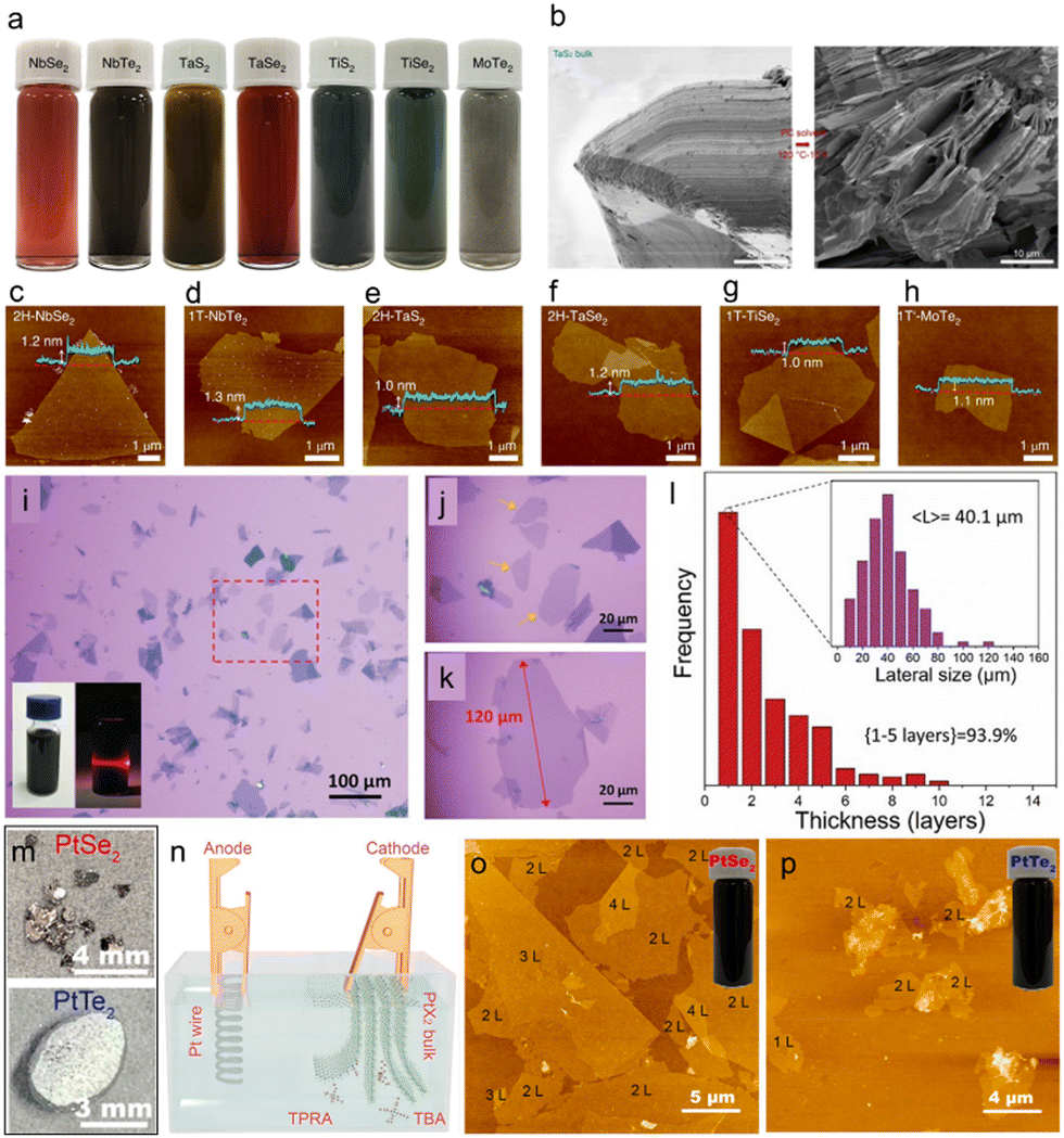 | ||
| Fig. 6 (a) Electrochemically exfoliated TMDs in PC. (b) SEM images of PC-exfoliated TaS2 bulks. (c)–(h) AFM images of exfoliated TMDs with corresponding height profiles. Reproduced with permission.152 Copyright 2020, Springer Nature (i)–(k) Optical image of exfoliated VSe2. (l) Thickness and lateral size distribution of the VSe2 nanosheets. Reproduced with permission.90 Copyright 2019, Wiley-VCH. (m) Photograph of PtSe2 and PtTe2 nanosheets. (n) Experimental setup for the electrochemical exfoliation of PtSe2 and PtTe2. (o) and (p) AFM image of the exfoliated PtSe2 and PtTe2 flakes on SiO2/Si substrate. Reproduced with permission.153 Copyright 2021, American Chemical Society. | ||
So far most of the reports are focussing on the ECE of groups IV, V and VI TMDs. However, recently Ma et al. reported the electrochemical cathodic exfoliation of group – X TMDs, such as PtSe2 and PtTe2.153 Both the bulk PtSe2 and PtTe2 crystals were first grown by chemical vapour transport method (Fig. 6(m)), then they were electrochemically exfoliated using either tetrapropylammonium (TPRA+) or tetrabutylammonium (TBA+) cations dissolved in the DMSO (Fig. 6(n)). An optimal yield of ∼44% bi-layer PtSe2 was achieved in an electrolyte consisting of 0.0025 M TPRA+ and by using a cathodic voltage of 6 V. The thickness of the majority of exfoliated PtSe2 and PtTe2 nanosheets was 1.2–1.5 nm, corresponding to bi-layer nanosheets. High stability of the material in air was observed (Fig. 6(o) and (p)). The bi-layer PtSe2 possessed an indirect bandgap of ∼0.23 eV, which is suitable for infrared optoelectronics. The excellent solution processability of the exfoliated PtSe2 and PtTe2 allowed fabrication of large scale photodetectors with excellent photodetection performance in the infrared region.
Finally, BPE has been applied to TMDs too: in 2017, Pumera et al. reported a direct synthesis method of 1T WS2 from commercial 2H WS2via bipolar exfoliation.119 An aqueous dispersion of 0.5 M Na2SO4 containing bulk 2H WS2 powder with a concentration of 0.5 mg mL−1 was used as an electrolyte. Intercalation and exfoliation of WS2 was completed by applying 10 V for 30 min under continuous stirring. A phase change from 2H to 1T phase was observed. The thickness of the as-exfoliated products range from 16 to 35 nm, showing lateral dimensions up to 0.5 μm. In a different work,154 the same research group extended the BPE to exfoliate tetrabutyl lithium (t-BuLi) intercalated MoSe2 in aqueous 0.5 M Na2SO4 solution. By applying a potential of 10 V between two Pt feeder electrodes for 30 minutes, exfoliated MoSe2 nanoparticles with sizes below 100 nm were obtained. However, due to the pre-intercalation of the bulk MoSe2 with t-BuLi, the exfoliated MoSe2 nanoparticles did show the 1T phase. Moreover, high-resolution XPS revealed that the exfoliated MoSe2 was oxidized due to the high potential during the BPE process. The as-produced MoSe2 nanoparticles were used as label for magneto-immunoassays toward protein detection. A similar bipolar electrochemical approach was also used to produce 1–5 layers of WSe2 nanoparticles with size of ∼100 nm.155
Overall, the ECE of TMDs has attracted strong research interest and has led to the publication of numerous studies focusing on different applications. A summary of the representative electrochemical synthesis of TMDs with key parameters, nanosheet properties and applications, is presented in Table 1. As shown, most of the applications are focused on electronics, with fewer studies on energy storage and catalysis and emerging applications in the biomedical field.
| Type | Material | Solvent | Electrolyte | Working potential/current | Thickness | Yield | Application type | Oxidationa | Ref. |
|---|---|---|---|---|---|---|---|---|---|
| a The oxidation of nanosheets is determined by the presence of a visible XPS peak of the oxidation state.AN = acetonitrile; DMSO = dimethyl sulfoxide; EC = ethylene carbonate; DC = dimethyl carbonate, PC = propylene carbonate, DMF = N,N-dimethylformamide; FET = field effect transistors; TFT = thin film transistor; HER = hydrogen evolution reaction. | |||||||||
| Anodic ECE | MoS2 | H2O | 0.5 M Na2SO4 | +10 V | 1–5 layers | 70% | FET | 15.6 at% | 66 |
| MoS2 | H2O | 1 M Na2SO4 | +20 V | Few-layer | — | Energy storage | Yes | 147 | |
| MoS2 | H2O | 0.5 M H2SO4 | +10 V | 1–3 layers | — | FET | Yes | 148 | |
| Cathodic ECE | MoS2 | H2O | 4 M KCl | −10 V | Few-layer | ∼30 wt% | Energy storage, catalysis | No | 162 |
| MoS2 | H2O | 0.5 M Na2SO4 | −10 V | 4 layers | — | Energy storage | No | 163 | |
| MoS2 | AN | 5 mg mL−1 THAB | −8 V | 1.5 nm | — | FET | No | 151 | |
| MoS2 | AN | 5 mg mL−1 THAB | −5 to −10 V | 3.8 ± 0.9 nm | — | FET/logic gates | No | 65 | |
| MoS2 | AN | 0.1 M TBABF4 | −10 V | 1–2 layers | >60% | Catalysis | No | 78 | |
| MoS2 | AN | 10 mg mL−1 THAB | −10 V | 1–2 layers | — | Photodetector | No | 164 | |
| MoS2 | AN | 10 mg mL−1 THAB | −12 V | 2–3 layers | — | Photodetector | No | 165 | |
| MoS2, HfS2 | AN | 5 mg mL−1 THAB | −7 V | ∼4 nm | — | FET, photodetector | MoS2 no | 81 and 82 | |
| HfS2 not mention | |||||||||
| WSe2, MoSe2, WS2, MoTe2 | AN | 5 mg mL−1 THAB | −15 V | 3–4 layers | — | TFT | No | 166 | |
| MoS2 | DMSO | 1 M LiCl | −5 V | 1–5 layers | — | FET | No | 144 | |
| 1T MoS2 | DMC/EC | 1 M LiClO4 | −4.5 V | 4.5 nm | >95% | HER, Supercapacitor | No | 102 | |
| 1T MoS2 | DMC/EC | 1 M LiPF6 | 0.7 V | Few layers | ∼80% | Supercapacitors | no | 146 | |
| 1T′ MoTe2 | PC/DMF | 0.001 M THACl/0.1 g L−1 PVP | −5 V | Monolayer | >95% | Mode-lock lasers | No | 145 | |
| MoS2, MoSe2, WS2, WSe2, MoTe2, WTe2 | Non-linear optics | ||||||||
| MoS2, WS2, WSe2 | PC | 5 mg mL−1 TPABr | −8 V | 10–14 nm | — | FETs | No | 167 | |
| MoS2 | AN | 5 mg mL−1 THAB | −10 V | 2.3 nm | — | Light emitting capacitor | No | 168 | |
| PtSe2, PtTe2 | DMSO | 0.0025 M TPA | −6 V | 1.2–1.5 nm | 44% | Photodetector | No | 153 | |
| MoS2, WS2, TiS2, TaS2, ZrS2 | EC/DMC | 1 M LiPF6 | 0.025–0.05 mA | Monolayer | >90% | FET | Yes | 143 | |
| NbSe2, WSe2 | EC/DMC | 1 M LiPF6 | 0.025–0.05 mA | <4 nm | — | FET | Yes | 143 | |
| VSe2 | PC | 0.005 M TPA | −4 to −2 V | 1–5 layers | >93% | — | No | 90 | |
| MoTe2, NbSe2, NbTe2, TaS2, TaSe2, TiS2, TiSe2 | PC | 0.05 M TBABF4 | −5 V | Monolayer | >75% | Superconducting wire arrays | No | 152 | |
| ReS2 | PC | 0.005 M THA, TPA | −5 V | Monolayer | 60% | — | No | 169 | |
| MoS2 | PC | 0.1 M TBA·HSO4 | −5 V | 6–10 layers | 70% | Biosensors | No | 170 | |
| Alternating bias ECE | MoS2 | H2O | 0.5 M K2SO4 | ±10 V | Few-layer | — | Catalysis | Yes | 171 |
| BPE | WS2 | H2O | 0.5 M Na2SO4 | 10 V | 16–35 nm | — | Biosensor | Yes | 119 |
| MoSe2, WSe2 | H2O | 0.5 M Na2SO4 | 10 V | 1–5 layers | — | Immuno-assay | Yes | 154 and 155 | |
3.3 MXene
Since the introduction of “MXene” in 2011,156 this class of materials has quickly expanded by including transition metal carbides, nitrides and carbonitrides. Unlike conventional 2DMs, which are exfoliated by overcoming the interlayer van der Waals (vdW) interactions, the production of MXene is achieved by selectively etching the A layers of the bulk MAX phase crystals, which have the general formula Mn+1AXn (n = 1, 2, 3), where M refers to transition metals (such as Ti, Sc, V, Cr, Mo, and Nb), A stands for group IIIA and IVA elements, and X represents carbon/nitrogen.157 As a result, MXenes have the chemical formula of Mn+1XnTx (n = 1, 2, 3), where Tx stands for the surface functional groups.158Typical MAX phase crystals have a layered hexagonal structure consisting of covalently bonded M–X layers with A elements interspersed between them via the metallic bond.159 Due to the nature of the metallic bond, the interaction between M and A is much stronger than that of the vdW forces, which makes it impossible to exfoliate the bulk crystal through conventional top-down methods. Traditionally, exfoliation is based on the use of hazardous etchants, such as hydrofluoric acid (HF) or fluoride-based compounds (LiF/HCl, NaHF2, KHF2).157 Clearly, it is important to find alternatives that do not involve the use of strong acids. In this framework, electrochemical etching was developed as a safer and environmentally friendly strategy to achieve rapid delamination. In 2018, Yang et al. reported a fluoride-free approach to fabricate Ti3C2Tx (Tx = OH, O) based on anodic etching of Ti3AlC2 with a yield of 60% (Fig. 7(a)).96 The exfoliation was conducted in an aqueous electrolyte containing 1.0 M NH4Cl and 0.2 M tetramethylammonium hydroxide (TMA·OH), with two Ti3AlC2 plates used as electrodes (Fig. 7(b)). During the process, Cl− anions rapidly etched the Al atoms and break the Ti–Al bonds under anodic potential (Ti3AlC2 − 3e− + 3Cl− = Ti3C2 + AlCl3). Subsequent intercalation of ammonium hydroxide further opens the edges of bulk crystals and facilitate the diffusion of Cl−, leading to complete etching of the surface. The lateral size of the nanosheets ranged from 1 to 5 μm with production of more than 90% of mono- and bi-layer Ti3C2Tx nanosheets with high crystallinity (Fig. 7(c)–(e)). Similarly, a thermo-assisted anodic etching method for Ti2CTx, Cr2CTx, and V2CTx was proposed by Pang et al. in 2019.160 The etching was conducted in 1 M HCl aqueous based electrolyte at a working potential of 0.3 V, and accelerated by gradually heating from 25 to 50 °C. The etched MXene sheets are further separated by sonication, resulting in multilayer nanosheets with a lateral size of up to 25 μm (average size of 1 μm).
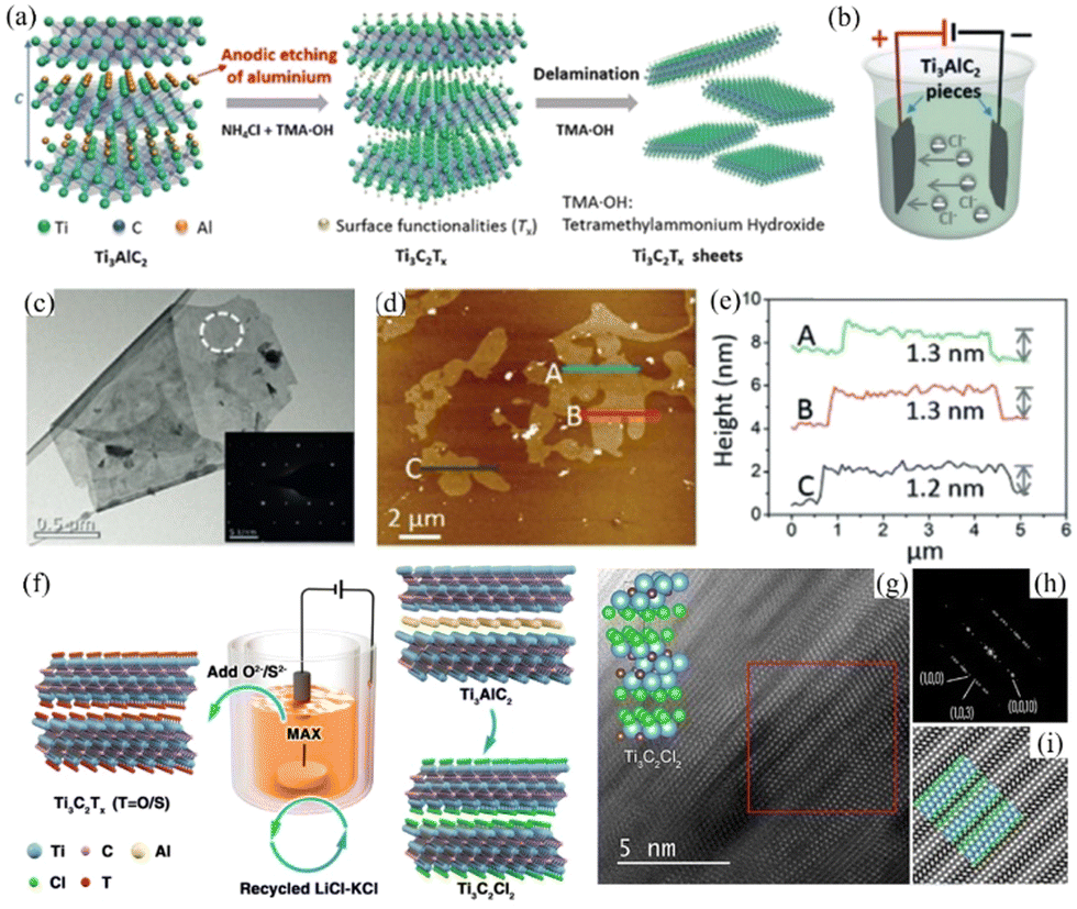 | ||
| Fig. 7 (a) Schematic illustration of anodic etching and delamination of Ti3AlC2. (b) Cell set up (c) TEM image and SAED pattern. (d and e) AFM image and relevant height profile. Reproduced with permission.96 Copyright 2018, Wiley-VCH (f) Schematic illustration of MS-E-etching. (g) High resolution STEM image of exfoliated Ti3C2Cl3via MS-E-etching; (h) and (i) Fourier transform and further emphasised structure of the labelled part of the micrograph. Reproduced with permission.172 Copyright 2021, Wiley-VCH. | ||
Besides aqueous-based electrolytes, ionic liquids were also investigated. Recently, Yin et al. developed a mild etching strategy to fabricate Ti3C2Fx nanosheets with controllable fluorination degree in ionic liquid electrolytes, which consisted of 1 M [BMIM][PF6] and 100 mL MeCN.161 Flakes with an average lateral size of 350 nm and a thickness of 3 nm were acquired after 5 h of etching at 5 V. By using the non-aqueous etching condition, the oxidation during the process was significantly restricted. Furthermore, Shen et al. proposed a synthetic route to produce MXene with controllable surface terminations via molten salt assisted anodic etching (MS-E-etching).172 As shown in Fig. 7(f), the etching cell consisted of a Ti3AlC2 anode and a nickel cathode. LiCl and KCl were mixed in a mass ratio of 1:1 and melted as an electrolyte. The etching was performed at 450 °C with 2 V of applied potential for 24 h in a high-purity argon protected glove box (Ti3AlC2 + 5LiCl (KCl) = Ti3C2Cl2 + 5Li (K) + AlCl3). After etching, the surface termination can be altered from Cl to O or S by directly adding Li2O or Li2S and reacting at 500 °C for another 10 h. STEM measurements confirmed the successful etching away of the Al layer and clearly showed the lamellar microstructure of produced Ti3C2Tx (Fig. 7(g)–(i)). The electrochemical properties of the products were tested by conducting cyclic voltammetry and galvanostatic charge–discharge experiments. MXenes with O terminated surface exhibited superior properties (rate performance 91.1% and capacitance retention 100% after 10000 cycles at 10 A g−1) compared with similar MXenes produced via other etching methods.
3.4 Post-transition metal chalcogenides
Layered PTMCs are composed of main group III to group VI post-transition metals (such as Ga, Ge, In, Sn, Sb, Bi) and chalcogen atoms (S, Se, Te). The 2D PTMCs have received increasing attention in recent years due to their high anisotropic and unique electronic structure, intriguing electronic and optoelectronic properties, that have been exploited in electrochemistry,173,174 photo-electrochemistry,175,176 electronics,177–179 gas sensing,180,181 and optoelectronics.182,183 For example, the semiconducting indium(III) selenide (In2Se3) exhibits a thickness dependent bandgap (1.3 eV for the bulk crystal and 2.8 eV for a single layer), covering the band gap range between the one of graphene and single layer TMDs. These crystals also display high absorption, broad range responsivity (from 325 nm to 1800 nm) and high sensitivity.In 2020, Shi et al. reported electrochemical cathodic exfoliation of In2Se3 using various tetraalkylammonium cations (TAA+, alkyl = methyl, ethyl, propyl, butyl, pentyl, heptyl and so on) in DMF.71 Among the various intercalating TAA+ cations studied, the methyl and ethyl alkyl groups do not show any significant volume expansion of the bulk crystals, due to their diameter (0.56–0.67 nm) being smaller than the interlayer spacing of In2Se3 (0.98 nm). However, the TAA+ cations containing propyl to octyl (0.78–1.2 nm) caused an ultrafast and substantial volume expansion of the In2Se3 bulk crystal. Among them, the THA+ (i.e. heptyl) cation showed the highest exfoliation efficiency because its diameter (~1 nm) matches well with the spacing of In2Se3. In addition to the different TAA+ cations, different polar aprotic solvents such as DMF, PC, NMP, and DMSO were also studied, and it was found that 0.1 M THA+ in DMF was the best electrolyte for exfoliating thin In2Se3 nanosheets due to the lower viscosity (0.92 mPa s) and higher dielectric constant (36.7) of DMF. As a result, a yield of 83% of exfoliated In2Se3 nanosheets with average flake size of 8.6 μm (up to 26 μm) and a mean thickness of 4.0 nm was obtained. Moreover, the absence of an InOx peak in the XPS spectra revealed the high purity and high structural integrity of the exfoliated In2Se3 nanosheets. Interestingly, the defect free In2Se3 nanosheets did not show degradation from air exposure for at least 2 weeks. Furthermore, solution processed large area thin film photodetectors fabricated using exfoliated In2Se3 (thickness 50 nm) showed a photoresponsivity of over 1 mA W−1 and ultrafast response time of 41 (rise) and 39 ms (decay) at 530 nm illumination. The dangling bond free contact between the exfoliated In2Se3 enabled efficient charge transport between individual nanosheets, which is essential for thin film optoelectronics. Similarly, Gao et al. reported the cathodic exfoliation of In2Se3 using THA+ ions in AN as electrolyte.184 A total of 90% of the exfoliated In2Se3 nanosheets were 2.2 nm thick, confirming the uniformity of the thickness. The XPS spectra revealed that the binding energy peaks of In 3d and Se 3d shifted to higher values compared to the bulk In2Se3 due to the n-type doping induced by the intercalation of THA+ ions. A thin film FET was demonstrated using tightly stacked L-b-L assembled thin In2Se3 films on silicon substrates, showing a field-effect mobility of 0.4 cm2 V−1 s−1 with on/off ratio of 7 × 10⁴. Whereas, field-effect transistors fabricated with a single In2Se3 flake showed a mobility of 12.8 cm2 V−1 s−1 and on/off ratio of 1.5 × 10³. Recently, Xue et al. reported the cathodic exfoliation of In2Se3 nanosheets using TBA+ ions in DMF.185 The exfoliated nanosheets showed high crystallinity with a statistical thickness distribution between 2–4 nm and a lateral size of up to 19.4 μm. Photo-electrochemical detectors fabricated by drop-casting as-exfoliated In2Se3 nanosheets showed good self-powered capability with broadband photoresponse from 365 to 850 nm and a high responsivity of 1.88 mA W−1 and a response time of 0.5 ms.
In 2020, Hao et al. reported the ECE of thin InSe nanosheets.186 Unlike most of the studies, which use TAA+ ions for intercalation, 0.01 M hexadecyltrimethylammonium bromide (CTAB) dissolved in NMP was used as the electrolyte (Fig. 8(a)). By applying a potential of −5 V for 2–4 hours, thin InSe nanosheets were obtained. The exfoliation resulted in a high yield (∼70%) of InSe, where ∼80% of the nanosheets were less than five layers thick and with lateral sizes ranging from tens of microns to 160 μm (avg. lateral size ∼28 μm) (Fig. 8(b)–(d)). Interestingly, after post-annealing at 300 °C, the InSe nanosheets showed enhanced photoluminescence emission due to the surface modification by carbon species (i.e., CTAB molecules) that escaped from the interlayer and the mono- and few layer InSe nanosheets during the annealing process. However, no obvious oxidation of the carbon modified InSe was detected, suggesting higher stability of the InSe nanosheets after post-annealing. Nevertheless, photodetectors fabricated with a single InSe nanosheet (∼7 nm thick) achieved a photoresponsivity of 2 A W−1, whereas a drop-cast InSe film with a thickness of ∼60 nm showed a photoresponsivity of ∼16 A W−1 when illuminated with a laser with 532 nm excitation wavelength. Furthermore, the thin InSe showed an average Hall mobility of 5.2 cm2 V−1 s−1. Additionally, the nanosheets can be scrolled using a solvent assisted assembly to form 1D nanoscrolls with an average height of 13 nm and a length of ∼46 μm (Fig. 8(e) and (f)).
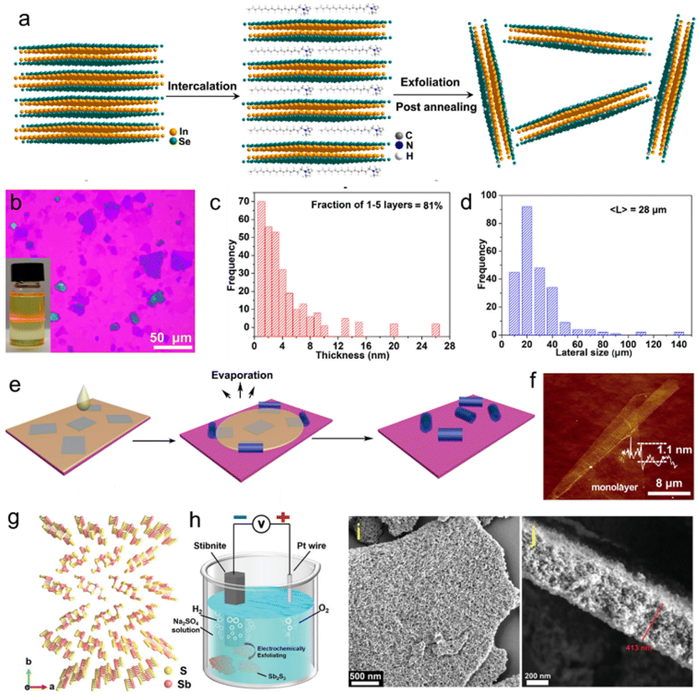 | ||
| Fig. 8 (a) Schematic illustration of the ECE process of InSe. (b) Optical microscopic image of the exfoliated InSe nanosheets on the silicon substrate. The inset of panel (b) shows a dispersion of InSe nanosheets in NMP. (c) and (d) Statistical analysis of the thickness and lateral sizes of InSe nanosheets. (e) Schematic illustration of the InSe nanoscroll preparation process. (f) AFM image of a rolled monolayer InSe nanosheet. Reproduced with permission.186 Copyright 2020 American Chemical Society. (g) The crystal structure of stibnite (Sb4S6)n: the yellow and pink spheres represent S and Sb atoms, respectively. (h) Schematic illustration of the experimental setup for ECE of the natural (Sb4S6)n. (i) SEM image of the Sb2S3 and (j) cross-sectional SEM image of the Sb2S3 flake. Reproduced with permission.70 Copyright 2022 Wiley-VCH. | ||
In addition to semiconductors, various topological insulating PTMCs, such as Bi2Se3, BiTe3, Sb2Te3 have also been successfully exfoliated by ECE. In 2016, Ambrosi et al. reported a simple and viable approach for the exfoliation of few layer Bi2Se3 and Bi2Te3 nanosheets.187 The exfoliation was carried out by using natural bulk Bi2Se3 and/or Bi2Te3 crystals placed onto a Cu tape as a working electrode, a Pt foil as a counter electrode and an aqueous solution of 0.5 M Na2SO4 as electrolyte. To avoid the direct physical contact of the Cu tape with the electrolyte solution and the exfoliated materials, while ensuring the ionic current flow, a dialysis membrane was applied to the Cu tape. Both Bi2Se3 and Bi2Te3 were exfoliated from their bulk counterparts when a combination of a preliminary anodic voltage of +10 V followed by a cathodic voltage of −10 V was used for 2 min. By repeating this combination of alternating applied potential, significant amounts of micron sized materials were released from the crystal. Due to the applied anodic potential, both Bi2Se3 and Bi2Te3 were found to be oxidized during the exfoliation process. In a different work, the same research group exfoliated Sb2Te3 using a similar electrochemical approach (i.e. applying a ±5 V anodic–cathodic intercalation strategy with aq. Na2SO4 electrolyte).188 However, in addition to the oxidation of as-prepared materials, the exfoliation strategy also resulted in the formation of small Sb2Te3 nanoparticles (<100 nm) together with flakes a few hundred nanometers in size. Recently, Li et al. reported the cathodic exfoliation of Sb2S3 using the naturally occurring layered mineral stibnite ((Sb4S6)n) as raw material (Fig. 8(g)).70 Using 1 M Na2SO4 solution as the electrolyte and applying a voltage of 5–10 V for 120 min, the Sb2S3 flakes were continuously exfoliated and dispersed in the electrolyte (Fig. 8(h)). Interestingly, the resulting Sb2S3 nanosheets showed a porous and hierarchical structure with a thickness of 413 nm and a lateral size ranging from 0.5 to 1.5 μm (Fig. 8(i) and (j)). The mechanism behind the formation of porous Sb2S3 involves a few steps: first, applying a bias voltage resulted in the random intercalation of H+ and Na+ ions into the interstices between the (Sb4S6)n moieties to lower the van der Waals force and thus causing the expansion and cracks of the stibnite. The reduction of H+ ions into H2 further weakened the vdW forces between (Sb4S6)n moieties leading to the expanded nanoparticles, which substantially agglomerate to reduce the surface energy because of the inter-particle attractive force. Second, when the ECE process continued for 30 min, more nanoparticles with reduced sizes assembled closer into a Sb2S3 flake. Although no distinct change in the size of nanoparticles was observed up to 60 min, the amount of nanopores gradually increased due to the strong agglomeration of nanoparticles. Finally, amorphous and hierarchical Sb2S3 was obtained after 120 min of the ECE process. As-prepared porous Sb2S3 nanosheets showed excellent gas sensing performances toward acetone at room temperature.
In addition to the cathodic and/or anodic exfoliation, BPE has also been applied for exfoliation of 2D PTMCs. In 2020, Tan et al. reported BPE of Sb2S3 and Bi2S3 by using 0.5 M Na2SO4 as a conductive electrolyte and applying 10 V between two electrodes.189 However, the exfoliation strategy resulted in rather thick Sb2S3 and Bi2S3 nanosheets (average thickness of 33.1 and 22.6 nm, respectively). Moreover, both exfoliated materials were found to be highly oxidized (oxygen content >10 at%).
3.5 Metal phosphorous trichalcogenides
MPTs are newly emerged layered materials with a general formula of MPX3 (where M = V, Mn, Fe, Co, Ni, Zn etc. and X = S, Se, Te), which contains layered structures with band gaps ranging from 1.3 to 3.5 eV,190–192 hence making these materials very attractive for applications in catalysis,193–195 batteries,196 gas storage,197 and optoelectronics,191,198,199 to name just a few examples. However, up to now the synthesis of 2D thin MPX3 crystals has been a big challenge. In this section, we summarize the recent progress on 2D MPX3 prepared by ECE.Although various 2D MPX3 materials, such as FePSe3,200 FePS3,191 NiPS3,195 MnPS3 and CdPS3,201 have been synthesized using LPE, in 2019 atomically thin and large size phase pure NiPS3 nanosheets with high crystallinity were prepared by cathodic exfoliation using TBABF4 in DMF (Fig. 9(a)).73,202 During the exfoliation process, the bulk NiPS3 crystals were significantly expanded by the gaseous species generated from the electrolyte decomposition. As-exfoliated atomically thin NiPS3 nanosheets could be readily dispersed in DMF by simple manual shaking rather than by ultra-sonication (Fig. 9(b)). Large size (average area of 150 μm2) and ∼70% of single layer phase pure NiPS3 nanosheets with high crystallinity were obtained (Fig. 9(c)–(e)). The exfoliated NiPS3 nanosheets showed high electrochemical activity. This was due to the fully exposed catalytic P and S active sites without any oxygen function groups within the exfoliated nanosheets.73 Moreover, the NiPS3 nanosheets also exhibited high photocurrent density, sensitive responsivity, cycling stability and excellent on/off behaviours under sunlight when used in a self-powered photo-electrochemical detector.202 Besides the ECE of high-quality NiPS3 nanosheets, Wang et al. demonstrated the electrochemical method to prepare heteroatom (e.g. B, C, N, and O) doped NiPS3.74 The cathodic ECE was performed using bulk NiPS3 crystals synthesized by the chemical vapour transfer method (Fig. 9(f) and (g)) in 0.05 M TBAPF6/DMF based electrolyte, resulting in thin NiPS3 nanosheets with a thickness below 2 nm (Fig. 9(h)–(j)). The exfoliated nanosheets did not show any evidence of oxidation during the exfoliation and were thermally stable up to 550 °C. The exfoliated material was then subjected to high temperature thermal annealing with various molecular precursors to obtain heteroatom doped-NiPS3 nanosheets. Furthermore, it was experimentally and theoretically demonstrated that C-doped NiPS3 shows HER activity similar to Pt with a low overpotential of 53.2 mV resulting in a current density of 10 mA cm−2 and a high exchange current density of 0.7 mA cm−2 in 1.0 M KOH. Additionally, several other studies have also demonstrated the successful exfoliation of NiPS3 nanosheets via cathodic exfoliation using TBAPF6 or LiPF6 based electrolytes and investigated their potential application in catalysis.72,203
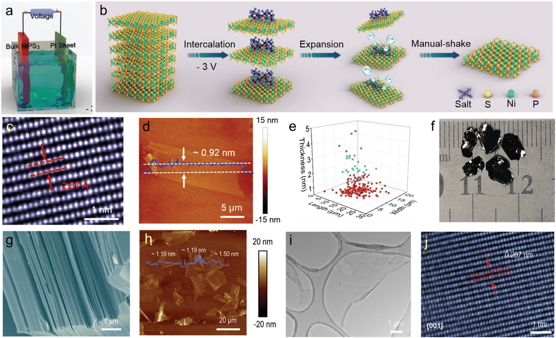 | ||
| Fig. 9 (a) Schematic illustration of the electrochemical setup for NiPS3 exfoliation. (b) Mechanism illustration of electrochemically exfoliating bulk NiPS3 crystals in tetra-n-butylammonium salts solution. (c) HRTEM image and (d) AFM image of large-sized and monolayer NiPS3 deposited on a silicon substrate. (e) Statistical analysis of the length, width, and thickness distribution of LSTL NiPS3. Reproduced with permission.73 Copyright 2019 Wiley-VCH. (f) and (g) Optical and SEM image of bulk NiPS3 crystals synthesized by chemical vapour transport method. (h) AFM image of the exfoliated NiPS3 flakes. (i) TEM and (j) HAADF STEM image of the exfoliated NiPS3 flake. The distance between two adjacent lattice fringes is 2.87 Å. Reproduced with permission.74 Copyright 2020 Wiley-VCH. | ||
Despite the current success of the NiPS3, many other 2D MPX3 are yet to be exfoliated by ECE.
3.6 Monoelemental 2D materials
The branch of the monoelemental 2DM family is composed of crystals made by a single chemical element, such as Si, Ge, Sn, P, Te, Bi, and B, whose crystals are referred as: silicene, germanene, stanine, phosphorene, tellurene, bismuthine and borophene, respectively. Most of these materials are semiconductors, making them interesting for applications in electronics and optoelectronics. This section shows the recent progress on electrochemically exfoliated monoelemental 2D materials.To date, various ECE methods have been developed to produce BP nanosheets. Despite the thermodynamic stability of BP, the presence of unpaired electrons in phosphorous atoms make the material unstable under ambient conditions. Once exposed to water, moisture, oxygen and visible light, the deterioration of BP occurs rapidly within a few hours,215 by significantly deteriorating its properties.216 In 2015, Erande et al. conducted the ECE of BP in a 0.5 M Na2SO4 aqueous solution and obtained few-layer nanosheets with a lateral dimension of 5–10 μm.217 Then, Pumera et al. developed a two-step anodic exfoliation method to acquire few-layer BP in 0.5 M H2SO4 in 2017.67 However, high resolution XPS revealed a strong POx peak of the exfoliated BP nanosheets, which is related to a high density of surface functional groups, indicating that BP is very sensitive to anodic oxidation. Recently, this feature has been utilised to fabricate porous phosphorene used as catalyst by Mei et al.218 The exfoliation was conducted by applying positive voltage (4 V) to the BP crystal anode in a 1 M H2SO4 aqueous electrolyte under ice bath conditions. A possible mechanism for the formation of a porous morphology has been attributed to the reduced oxidation rate caused by the use of low temperatures. During the exfoliation, the SO42− ions are activated by the external field and transferred into sulfate radicals with strong oxidising capability. These radicals attack the edge of BP layers and open the boundary for further intercalation and enlarge the interlayer spacing. The rate of boundary expansion is suppressed at low temperatures, allowing more time for the oxidising sulfate radicals to react with the relatively highly reactive in-plane P atoms before the nanosheets is falling apart from the anode. This leads to the formation of POx, which can further react with water to form soluble H3PO4 and create holes in the BP nanosheets.219 The nanosheets have a lateral size and thickness of 0.3–1.4 μm and 1–2 nm, respectively. The pore size can be altered from 20 to 100 nm by adjusting the applied voltage. XPS revealed a significant drop in the intensity of the P–O peak compared with previous reports, which further confirmed that the oxidation rate has decreased, and that the elimination of highly reactive regions succeeded in reducing the density of surface oxidation on the final product. The nanosheets were finally tested for nitrogen reduction reaction, providing a NH3 yield of 46.04 μg h−1 mgcat−1. with a faradaic efficiency of 8.78%. Although significant research efforts have been made to anodic exfoliation of BP nanosheets, preventing the oxidation of the BP during the exfoliation process remains a major challenge.
Due to the high sensitivity of BP towards anodic oxidation, cathodic exfoliation has been widely used to preserve the crystalline quality of the material. In contrast with anodic exfoliation, cathodic exfoliation does not involve the generation of oxygen-containing free radicals, therefore resulting in BP nanosheets with no surface defects and functional groups. ECE in quaternary ammonium and many organic solvents has been systematically studied over the past few years. For example, in 2017 Huang et al. produced few-layer BP nanosheets of large area without surface functional groups via cathodic exfoliation in a DMF based electrolyte using TBAPF6 as an intercalant.220 The modulation of the working potential from −2.5 to −15 V was used to control the intercalation process of TBA+ ions. XPS confirmed the production of high-quality phosphorene. Following this work, subsequent research on cathodic ECE of BP focused on the intercalation of ammonium salts with different chain lengths dissolved in different solvents. Similarly, Xiao et al. reported the production of oxygen-free BP nanosheets using a PC solution of TBAPF6 as an electrolyte. The exfoliated BP nanosheets have thickness of 2–7 nm.221 In 2018, Li et al. investigated the cathodic exfoliation of BP using 0.01 M TBABF4 in DMSO as an electrolyte to intercalate the BP crystal using an applied voltage of −5 V.138 The electrochemical intercalation and BP crystal expansion processes were observed in a microelectrochemical cell under an optical microscope. Most of the exfoliated BP nanosheets consist of 1–5 layers with an average dimension of 10 μm2. Due to the high-quality of the exfoliated nanosheets, a hole mobility of up to 100 cm2 V−1 s−1 was achieved on a single BP flake-based FET device. Yang et al. systematically investigated the scalable exfoliation process for achieving high-quality and defect-free BP using various alkali ions (e.g. Li+, Na+ and K+) and tetraalkylammonium (alkyl = methyl, ethyl and n-butyl) cations in PC.68 The quaternary ammonium cation based electrolyte, especially tetra-n-butylammonium bisulfate (TBAHSO4), displayed superior exfoliation efficiency to alkali ions in terms of speed of intercalation and yield of exfoliation (Fig. 10(b)). The variable diameter of TBA+ ions (i.e., 0.47–0.89 nm) matches the interlayer distance of BP (0.53 nm) and the penetration of TBA+ ions accompanied by the reduction of solvated protons (HSO4− ⇌ SO42− + H+, 2H+ + 2e− → H2) further (Fig. 10(a)) accelerated the exfoliation, leading to high yield (up to 78%) with an average dimension of 4 μm2 (Fig. 10(c)). Furthermore, HRTEM images of the exfoliated BP nanosheets show an intact lattice structure (Fig. 10(d)) without any evidence of oxidation. As a result, FET devices based on a single BP flake revealed a remarkable hole mobility of 252 ± 18 cm2 V−1 s−1 with an on/off ratio of 1.2 × 10⁵ at 143 K under vacuum. In a recent work, Kovalska et al. proposed a low-potential cathodic exfoliation method for the preparation of few-layer phosphorene with nearly 100% yield.222 The exfoliation was performed in a DMF solution of 0.01 M TBAPF6 under the action of three stages of negative potential. First, a voltage of −1 V and −2.5 V was applied to the working electrode for 2 min each to promote proper wetting and accumulation of the anions around the cathode. Then, a voltage of −3.8 V was applied for 5 h to promote the intercalation. The highly accurate potential control prevented damage during delamination, leading to highly crystalline products with lateral dimensions of up to 25 μm and a thickness of 1–5 layers.
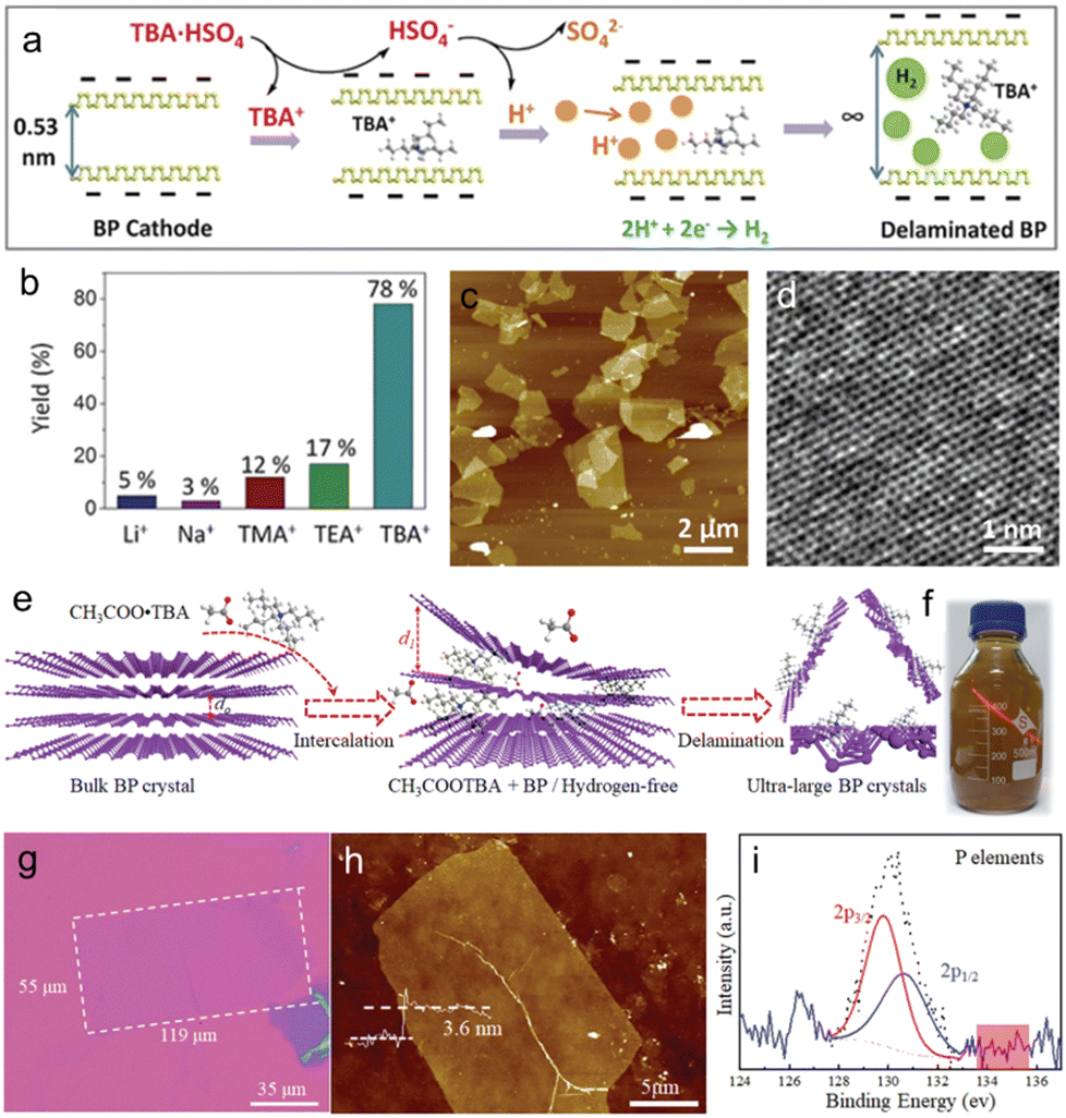 | ||
| Fig. 10 (a) Illustrative mechanism of the THA·HSO4 intercalation process in the BP electrode. (b) Yield of BP nanosheets obtained by ECE using different intercalating cations. (c) and (d) AFM and HRTEM images of the exfoliated BP nanosheets, respectively. Reproduced with permission.68 Copyright 2018, Wiley-VCH. (e) Schematic illustration of the exfoliation process of BP using CH3COOTBA as an intercalant. (f) DMF dispersion of exfoliated BP showing Tyndall effect. (g) Optical image of a thin BP nanosheet with a domain size of 119 μm. (h) Typical AFM image of the exfoliated BP nanosheets. (i) High-resolution XPS spectra of P as-exfoliated BP nanosheets. Reproduced with permission.223 Copyright 2020, Wiley-VCH. | ||
Moreover, to further understand the mechanism of intercalation, Wang et al. delved into the role of coordination anions in cathode exfoliation and succeeded in obtaining several-layers BP nanosheets of large size.223 The effect of the H+ ionisation constant on the domain size of products was investigated by using CH3COOTBA, TBAHSO4 and TBAH2PO4 as intercalants. Experiments confirmed that a higher concentration of H+ will promote the generation of H2 by-product, leading to faster delamination and production of nanosheets of smaller domain size. Results indicate the high electronegativity of halide anions and its strong interaction with TBA+ will promote the P atoms donating electrons to intercalants, resulting in large electron-deficient areas in BP crystal, leading to unstable P–P bonds and decreased domain size. Fig. 10(e) schematically illustrates the optimum delamination process, using a DMF solution of 2.0 mM CH3COOTBA as an electrolyte and a working potential of −20 V. An image of the obtained BP dispersion is shown in Fig. 10(f). AFM and optical microscopy characterisations showed that the nanosheets have an average lateral size of 77.6 ± 15.0 μm and an average thickness of 4.1 nm (Fig. 10(g) and (h)). The Raman spectra of the exfoliated BP nanosheets show that the exfoliation process is non-destructive, as further confirmed by HRTEM, confirming the high crystallinity of the material. Besides, XPS reveals the absence of peaks around 133 eV, which further demonstrates the non-oxidative nature of the exfoliation process (Fig. 10(i)). Further electronic transport measurements showed that the nanosheets have a hole mobility of 76 cm2 V−1 s−1 and an on/off ratio of ≈1.2 × 10³ measured at room temperature and under vacuum.
The cathodic exfoliation in an aqueous environment with polymer intercalant has also been studied in the past few years. Very recently, He et al. reported an environmentally friendly cathodic ECE approach to simultaneously exfoliate and improve the interfacial adhesion of few-layer BP for the fabrication of high-performance nanocomposites.224 The exfoliation was conducted in an aqueous solution of 5 wt% ethylene imine polymer (PEI). A bias of −8 V was applied for 30 min to drive the intercalation. During the process, H+ and PEI(H+)m, which are generated by dissolved PEI and conversion of water, acted as intercalating species. Meanwhile, the H2 bubbles formed from intercalated H+ further separated the nanosheets from the bulk BP crystal, leading to 3–5 μm lateral size of few-layer BP nanosheets. After delamination, dissolved PEI naturally adsorbs on the surface of the flakes through electrostatic attraction, preventing the exfoliated BP nanosheets from aggregation and possible oxidation due to contact with water and oxygen, and enhancing the interfacial adhesion with the waterborne polyurathane matrix.225
Among all ECE methods, the majority of them require additives as intercalants. However, Baboukani et al. reported BPE using a BP bar as a bipolar electrode and pure DI water as an electrolyte.108 Nanosheets with a lateral size of hundreds of nanometres and a thickness of 3 to 5 layers were obtained by applying a voltage of 30 V for 24 h. However, XPS showed a board peak at 133.0 eV, indicating a relatively high degree of oxidation.
In recent years, BP nanosheets with other dimensionalities, such as nanobelts or nanoribbons have been electrochemically exfoliated by choosing suitable parameters such as the size of the intercalants and applied potential of the cathodic electrochemical process.226 For example, Liu et al. developed the anodic ECE to prepare zigzag-BP nanobelts (z-PNBs), nanoflakes and quantum dots from bulk BP via intercalating BF4− ions dissolving in water and changing the current densities of 0.1 to 0.5 A cm−2.227 BP nanosheets are produced when the current density was less than 0.1 A cm−2 (Fig. 11(a)). However, the quantum dots were obtained (Fig. 11(b)) when the current density was ∼0.5 A cm−2, while z-PNBs were produced (Fig. 11(c) and (d)) when the current density was in the range was 0.2–0.3 A cm−2. The size distribution of z-PNBs indicated that the aspect ratio (measured as length over width) of as-prepared nanobelts was generally larger than 10 (Fig. 11(e)). The formation process of z-PNBs can be divided into two steps: ionic intercalation and oxygen degradation (Fig. 11(f)). During the electrochemical process, the BF4− ions intercalated between the bulk BP layers, along the a-axis oriented channels, i.e. [100] direction. The BF4− ion intercalation process was demonstrated by the chronopotentiometry measurements at different current densities ranging from −0.1 to 0.5 A cm−2 during the ECE process. During intercalation, the chemisorbed O2 dissociates on the surface of the pristine BP, which is then followed by the formation of H2 bonds between dangling oxygen and water molecules as well as the electronic hydrolysis of P–O–P. These steps lead to the unzipping of P–P bonds. The FETs fabricated with the prepared z-PNBS displayed n-type behaviour with an electron mobility of 87 cm2 V−1 s−1. Similarly, Yu et al. produced BP nanoribbons via facile cathodic ECE using two types of quaternary ammonium cations (i.e. TPA+ and THA+) dissolved in PC as electrolytes and intercalating species.228 The exfoliation process was performed in an Ar protected glovebox to avoid oxidation of BP nanoribbons. It was found that the intercalation of smaller sized TPA+ ions resulted in an improved yield of BP nanoribbons compared with THA+. It is suggested that using a lower intercalation voltage can further increase the yield. The strain created by the ions intercalated into the BP crystal, causing a slit along the zigzag direction that opened up like a zip as the further ions are intercalated. A moderate strain favoured the P–P bonds’ dissociation along the zigzag direction leading to a nanoribbon dominated exfoliation. However, applying excessive strain on BP overrides the energy differences between P–P bonds in both zigzag and armchair directions, resulting in un-controlled exfoliation (Fig. 11(g)). About 90% of the exfoliated BP nanoribbons were between 1.3 nm to 10 nm thick (Fig. 11(h)), and the length of the nanoribbons was >100 μm with an aspect ratio >100 (Fig. 11(i) and (j)).
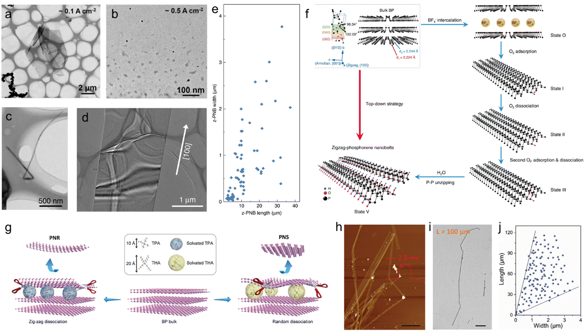 | ||
| Fig. 11 TEM images of phosphorene: (a) nanosheets and (b) quantum dots, respectively. TEM images of: (c) a single z-PNB twisted and (d) with the zigzag [100] direction, respectively. (e) Length as a function of width of z-PNBs. (f) Schematic illustration of the exfoliation mechanism of z-PNBs. Reproduced with permission.227 Copyright 2020 Springer Nature. (g) Schematic illustration of the proposed exfoliation mechanism of BP nanoribbons and nanosheets. (h) AFM image of few layer BP nanoribbons with height of 2.5 nm. (i) SEM image of a long nanoribbon with length >100 μm. (j) Statistical analysis on length and width distribution of 135 BP nanoribbons. Reproduced with permission.228 Copyright 2021 Wiley-VCH. | ||
In general, production of high-quality monolayer phosphorene by both traditional ECE and BPE remains a challenge. However, other nanostructured forms of BP with potential for practical applications have been successfully demonstrated by ECE.
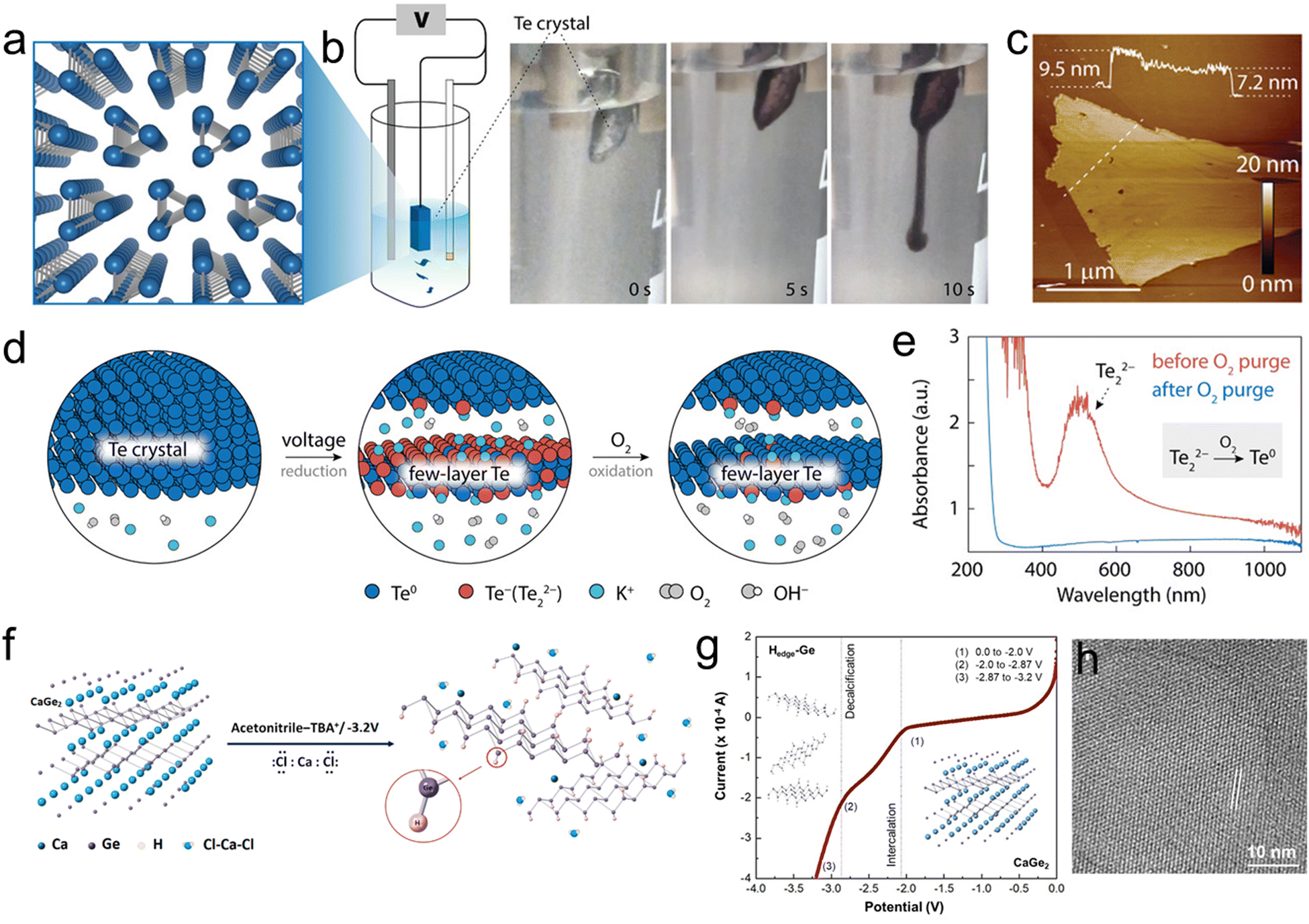 | ||
| Fig. 12 (a) Illustration of the Te crystalline structure, (b) Setup for ECE of the Te crystal, and the digital photos of the exfoliation process at different exfoliation times: 0, 5 and 10 s. (c) AFM image of exfoliated Te nanosheets. (d) Proposed mechanism of ECE of Te crystals in aqueous alkaline solution. (e) UV-Vis spectra of exfoliated Te nanosheets before and after O2 purge. Reproduced with permission.229 Copyright 2021 Wiley-VCH. (f) Schematic diagram of ECE of CaGe2 crystal towards few layer Hedge-Ge nanosheets. (g) The experimental LSV curve recorded during the ECE of CaGe2 in 0.01 M TBACl/AN at −3.2 V. The potential ranges from 0 to −2.0 V (1), −2.0 to −2.87 V (2), and −2.87 to −3.2 V corresponds to the intercalation, decalcification and exfoliation processes. (h) HRTEM image of the exfoliated Hedge-Ge nanosheet. The distance between the in-plane Ge atoms is 0.54 nm and is marked by two white parallel lines. Reproduced with permission.76 Copyright 2021 American Chemical Society. | ||
Moving to arsenene, in 2020, Kovalska et al. reported cathodic ECE of a few layered arsenene from bulk black arsenic using 1 M ammonium hexafluorophosphate (NH4PF6) in anhydrous DMF.75 The exfoliated arsenene nanosheets showed a net-like porous structure with a thickness of ∼0.6 nm and a lateral size of ∼1.5 μm. However, the exfoliated nanosheets exhibited a tendency for self-aggregation during post-exfoliation processing and tend to interact with air.
Recently, few layer silicene nanosheets were also exfoliated by using the electrochemical Li+ ion intercalation/delithiation process in protic solvents.230 It was found that solvent selection in the delithiation process played a critical role in the structure evolution of the final products. Silicene nanosheets with a size of 30–100 nm and a thickness of ∼2.4 nm in were dispersed in isopropyl alcohol.
In 2017, Lu et al. reported for the first time the cathodic ECE of antimonene nanosheets using 0.2 M Na2SO4 aqueous solution as an electrolyte.77 The obtained few layer Sb nanosheets have an average thickness of 31.6 nm and a lateral size of ≈10 μm. The nanosheets showed excellent stability under ambient conditions for months. Additionally, Li et al. also reported the cathodic exfoliation of Sb nanosheets by Na+ ion intercalation that resulted in 60% of the exfoliated nanosheets less than four layers with good crystallinity.231 ECE with an alternating bias was also reported to produce Sb nanosheets.188 The exfoliation was performed in both Na2SO4 or Li2SO4 (0.5 M) electrolytes by applying an alternating anodic–cathodic potential of ±5 V. However, the exfoliated Sb was found to be highly oxidized.
In 2019, Wu et al. successfully exfoliated 2D bismuth nanosheets, using an industrial Bi ingot.232 The electrochemical cathodic exfoliation was carried out in an electrochemical cell containing a graphite rod as an anode and TPA+ ions dissolved in AN as an electrolyte. With an applied voltage of −10 V, the Bi ingot was rapidly exfoliated within 10 s. During the initial stage of the exfoliation, the solvated TPA complex with TPA+ ions and AN solvent molecules co-intercalated into the interlayer spacing of bulk Bi causing the expansion of the layered structure. Afterwards, the electrochemical decomposition of the intercalated species resulted in the formation of gaseous species enabling the rapid exfoliation of the thin Bi nanosheets. The average thickness of the exfoliated Bi nanosheets was 2–4 nm, corresponding to 6–10 layers. Detailed characterization revealed high crystallinity of the Bi nanosheets without any oxidation. As exfoliated Bi nanosheets exhibited high selectivity for formic acid generation over a wide potential range from −0.77 to −1.17 V with a high current density and adequate durability. Later in 2021, Basyouni et al. reported the cathodic exfoliation of bismuthine in aqueous Na2SO4 electrolyte.233 When a negative voltage of −6 or −10 V on the bulk Bi electrode was applied, the Na+ ions were intercalated into the Bi layers causing the interlayer expansion and exfoliation of bismuth into bismuthine. The average thickness of the exfoliated Bi nanosheets was 6.0 nm with a lateral size between 20 and 100 nm.
Kovalska et al. demonstrated the one-step synthesis of edge-hydrogenated germanene (Hedge-Ge) by low potential ECE of CaGe2 in 0.01 M TBACl in AN (Fig. 12(f)).76 The exfoliation was based on simultaneous intercalation and decalcification processes. The intercalation of TBA+ ions into CaGe2 inter-layers started at a potential of −2.2 V, followed by a decalcification process at −2.87 V leading to the exfoliation of germanene at −3.2 V. The potential −2.87 V corresponded to the reduction potential of Ca2+ ions (Fig. 12(g)). Detailed characterization of the materials revealed successful exfoliation of micrometre size single- and few-layer Ge with good crystallinity (Fig. 12(h)). The exfoliated Ge nanosheets were tested for the detection of several volatile organic compounds.
Recently, Sielicki et al. reported the ECE of nonconductive boron to few-layered borophene.95 The exfoliation was achieved by incorporating the bulk boron into a Cu and/or Ni metal mesh to induce electrical conductivity. It was found that when Na2SO4 was used as an electrolyte, the thickness of the exfoliated borophene flakes depends on the type of metal mesh used. Using a Cu mesh to induce electricity into bulk boron, resulted in thinner borophene nanosheets (2.70–4.97 nm) compared to the Ni mesh (thickness 13–26 nm). Moreover, the use of metal mesh for the exfoliation significantly affects the crystallinity of the exfoliated borophene and can be either single crystalline or polycrystalline for Cu or Ni, respectively. Nevertheless, the exfoliation process reported in this work provides a route to exfoliate other nonconductive materials into their 2D forms.
3.7 Other 2D materials
In addition to the different classes of 2DMs discussed above, in recent years, the ECE has been applied to a wide range of less studied 2DMs, for example, bismuth tellurohalides (BiTeX; X = Cl−, Br−, I−etc.), a group of layered materials with strong spin–orbit coupling. Among them, bismuth telluride iodide (BiTeI), whose structure is shown in Fig. 13(a), has been electrochemically exfoliated using both TBAPF6 and LiPF6 dissolved in DMF as the electrolyte (Fig. 13(b) and (c)).234 The exfoliation of BiTeI was achieved in three steps: (i) first, −1 V bias was applied for 2 min to wet the bulk crystal, (ii) then, it was changed to −2.5 V for another 2 min to accumulate the TBA+/Li+ cations on the BiTeI crystal and (iii) finally, it was changed to −3.8 V in order to intercalate TBA+/Li+ ions and dissociate BiTeI into thin nanosheets. It was found that the use of Li+ ions as intercalating species results in a milder exfoliation process but with thicker BiTeI nanosheets. The BiTeI nanosheets exfoliated in TBA+ ions have a thickness between 5–18 nm, whereas the intercalation of Li+ resulted in BiTeI nanosheets with a thickness of 15–25 nm. The exfoliated nanosheets showed minor topological etching of iodine atoms and formation of bismuth oxides on the surface of the exfoliated material. Nevertheless, when used as a catalyst for the nitrogen reduction reaction, BiTeI showed high performance, achieving an NH3 yield of 1.0 μg h−1 cm−1 and a faradaic efficiency of 1.67% at −5.0 V vs. Ag/AgCl.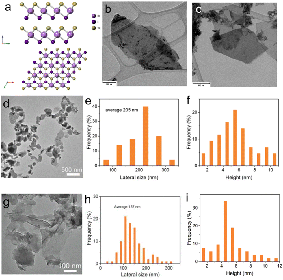 | ||
| Fig. 13 (a) Side and top view of the BiTeI crystal structure. (b) and (c) TEM images of the BiTeI nanosheets exfoliated in TBAPF6 and LiPF6 ions, respectively. Reproduced with permission.234 Copyright 2021 American Chemical Society. (d) SEM image of the exfoliated MnO2 nanosheets. (e) and (f) Statistical distribution of lateral size and thickness of MnO2 nanosheets, respectively (g) TEM image of exfoliated g-C3N4 nanosheets. (h) and (i) Statistical distribution of the lateral size and thickness of g-C3N4 nanosheets, respectively. Reproduced with permission.78 Copyright 2018 Wiley-VCH. | ||
Recently, Lam et al. reported the ECE of α-RuCl3, a layered transition metal halide possessing a range of exotic electronic, optical and magnetic properties, including fractional excitations indicative of a proximate Kitaev quantum spin liquid.235 α-RuCl3 was exfoliated through an electrochemically assisted LPE approach, where large THA+ ions dissolved in acetonitrile were electrochemically intercalated by applying a negative bias to the α-RuCl3 crystal. XRD revealed that the intercalation of THA+ ions significantly increased the interlayer spacing of the bulk α-RuCl3 from 6.0 to 24.9 Å. The THA+ intercalated α-RuCl3 crystal was then exfoliated into thin 2D nanosheets by bath sonication in N-cyclohexyl-2-pyrrolidone without the need for any additional stabilizer or surfactant. The exfoliated nanosheets have high crystallinity with an average thickness and lateral size of ∼2 nm and ∼200 nm, respectively. Both the sheet resistance and magnetoresistance measurements revealed a phase transition of α-RuCl3 at 230 K due to the enhanced electron–electron correlations resulting from the intercalation induced electron doping.235 In addition, magnetic susceptibility measurements showed an antiferromagnetic transition for α-RuCl3 at 2.6 K. Furthermore, the intercalation induced doping broadens the optical absorption range, enabling large area NIR photodetectors with highly linear photocurrent response.
Recently, Kovalska et al. successfully performed cathodic ECE of 2D siligene (SiGe) from a Zintle phase Ca1.5SiGe1.0 crystal in an oxygen-free environment and with an electrolyte containing 0.3 M tetrabutylammonium perchlorate (TBAClO4) in AN.236 The 2D SiGe exfoliation mechanism was founded on the decalcification–intercalation mechanism, where Ca undergoes reduction–oxidation reactions. The exfoliation mechanism occurred in three separate stages with different applied voltages. The first two stages involve the amassing of TBA+ cations toward the layered CaSiGe at an applied potential of −2.0 V and the decalcification–intercalation persuaded by the reduction of Ca2+ and TBA+ ion propagation at −2.87 V. Subsequently, 2D SiGe nanosheets were exfoliated in the third stage at an applied potential of −3.8 V. Thin, uniform and contamination free SiGe nanosheets with lateral size between 1–2 μm were obtained with nearly 100% yield. Detailed material characterisation revealed that the exfoliated few layer SiGe possesses semiconducting rather than metallic properties caused by the interlayer hydrogenation. Moreover, XPS spectroscopy revealed that the SiGe nanosheets are slightly oxidized since Ge atoms are more favourable to the oxygen species rather than Si atoms. The SiGe nanosheets were explored as an anode material for Li-ion batteries, showing a 10% increment of the specific capacity.
In 2018, Li et al. reported the successful production of 2D MnO2 and graphitic carbon nitride (g-C3N4) by ECE.78 The brinessite-type-δ-MnO2 was cathodically exfoliated by using TBA+ ions containing electrolyte, resulting in an exfoliation yield of ∼60% with an average nanosheet size of 205 nm and a thickness of 5 nm (Fig. 13(d)–(f)). While exfoliation of g-C3N4 nanosheets using 1-butyl-1-methylpyrrolidinium (Py1,4+) as an electrolyte, resulted in 4–6 nm thick g-C3N4 nanosheets with lateral sizes of 137 nm (Fig. 13(g)–(i)). Composites of graphene with exfoliated MnO2 and/or g-C3N4 were further investigated for their potential applications in supercapacitors and HER, respectively.
In 2020, Deleep et al. successfully exfoliated layered metal hydroxides such as β-Co(OH)2 using BPE, where bulk Co(OH)2 powder was mixed with aqueous Na2SO4 (0.5 M) based electrolyte.237 The colour of the bulk Co(OH)2 solution changes from pink to brown indicated the partial oxidation of the Co(OH)2 (Co2+) state to the CoOOH (Co3+) state. As exfoliated β-Co(OH)2 nanosheets showed an average thickness of ∼7.4 nm. However, XPS revealed the presence of a small peak in the Co3+ state implying the oxidation of the material. Nevertheless, the exfoliated β-Co(OH)2 nanosheets exhibited enhanced electrocatalytic activity toward OER with a very low overpotential of 390 mV at 10 mA cm−2 in alkaline medium. BPE has also been used to exfoliate molybdenum boride (Mo2B5) and tungsten boride (W2B5) by applying a constant DC potential across two Pt driving electrodes to the electrolyte solution.238 As exfoliated, Mo2B5 and W2B5 revealed lateral sizes up to a few microns. The XPS results of the bulk Mo2B5 suggested the presence of surface oxidation in the exfoliated materials, however after the exfoliation, the presence of Mo0 and B0 states suggested that the electrochemical treatment exposed a new surface of Mo2B5 or removed the oxidized surface contaminants. On the other hand, the XPS spectra of W2B5 showed the presence of bipolar induced oxidation of W but the B 1s peak remained unchanged in the B0 state despite the oxidation of W.
4. Conclusions and perspectives
ECE has become one of the mainstream methods to prepare solution processed 2DMs of large size and thickness down to a few layers. After being successfully applied to the production of graphene, this approach has been demonstrated to be a viable route for the production of many 2DMs, from TMDs (Table 1) to BP, hBN, MXene, MOF, group III–V binary compounds and other less explored 2DMs (Table 2).| Type | Material | Solvent | Electrolyte | Working potential/current | Thickness | Yield | Size | Application | Ref. |
|---|---|---|---|---|---|---|---|---|---|
| Anodic exfoliation | BP | H2O | 0.5 M Na2SO4 | +7 V | 1–5 nm | — | 5–10 μm | — | 217 |
| BP | H2O | 0.5 M H2SO4 | +3 V | Few-layer | — | — | — | 67 | |
| BP | H2O | 1 M H2SO4 | +4 V | l–2 nm | — | 0.3–1.4 μm | Catalysis | 218 | |
| BP | H2O | 0.1 M Phytic acid | +10 V | 6.08 nm | — | — | Fire resistance coating | 239 | |
| Ti3C2Tx | H2O | 1 M NH4Cl and 0.2 M TMA·OH | +5 V | Monolayer | 90% | 1–5 μm | Energy storage | 96 | |
| Ti3C2Fx | AN | 1 M [BMIM][PF6] | +5 V | 3 nm | — | 350 nm | Energy storage | 161 | |
| Ti3C2Tx | — | 1:1 Melt LiCl/KCl |
+2 V | Few-layer | — | — | Energy storage | 172 | |
| Ti2CTx, Cr2CTx, V2CTx | H2O | 1 M HCl | +0.3 V | Few-layer | ∼50% | 1 μm | Catalysis | 160 | |
| Borophene (B) | H2O | 1 M Na2SO4 | 0.1–1 A | 2–26 nm | — | 0.11–1.47 μm | — | 95 | |
| Cathodic exfoliation | hBN | DMC/EC | 1 M LiPF6 | 0.025 mA | 2–8 nm | — | 730 nm | — | 118 |
| BP | DMF | 0.01 M TBAPF6 | −2.5 to −15 V | 2–11 layers | — | ∼15 μm | Sodium-ion batteries | 220 | |
| BP | DMF | 0.01 M TBAPF6 | −3.8 V | 1–5 layers | 100% | < 25 μm | Optoelectronics | 222 | |
| BP | DMF | 2.0 mM CH3COOTBA | −20 V | 4.1 nm | 81% | 77.6 ± 15.0 μm | FET | 223 | |
| BP | PC | 0.1 M TBAPF6 | −30 V | 2–7 nm | — | — | — | 221 | |
| BP | PC | 0.1 M TBA·HSO4 | −8 V | 3.7 ± 1.3 nm | 78% | 4 μm2 | FET | 68 | |
| BP | DMSO | 0.001 M TBABF4 | −5 V | 1–5 layers | >80% | 10 μm2 | FET | 138 | |
| BP | H2O | 5 wt% PEI | −8 V | Few-layer | — | 3–5 μm | Composite | 224 | |
| BP | DMF | 0.05 M TBPBr | −5 V | ∼4 nm | — | Tens of micrometres | Energy Storage | 240 | |
| BP | H2O | 0.5 M CTAC | −30 V | 5–8 nm | ∼37% | Few micrometres | — | 241 | |
| BP nano ribbons | H2O | 1/3 volume [BMIM]BF4 | 0.1–0.5 A cm−2 | 1–8 layers | ∼90% | Width ∼4 μm Length ∼40 μm | FET | 227 | |
| BP nano belts | PC | 0.01 M TPACl | −5 V | Few-layer | >80% | Length 100 μm | Lithium metal batteries | 228 | |
| In2Se3 | DMF | 0.05 M TBABr | −5 V | 2–4 nm | — | ∼19.4 μm | Optoelectronics | 185 | |
| In2Se3 | DMF | 0.1 M THABr | −5 V | 4.0 nm | 83% | 8.6 μm | Optoelectronics | 71 | |
| In2Se3 | AN | 5 mg mL−1 THABr | −8 V | 2.2 nm | 90% | Few micrometres | FET | 184 | |
| InSe | NMP | 0.01 M CTAB | −5 V | ∼5 layers | 70% | 28 μm | Optoelectronic | 186 | |
| Sb2S3 | H2O | 1 M Na2SO4 | −5 to −10 V | 413 nm | — | 0.5–1.5 μm | Gas sensing | 70 | |
| NiPS3 | DMF | 0.05 M TBABF4 | −3 V | Monolayer | ∼80% | 150 μm2 | Catalysis | 73 | |
| NiPS3 | DMF | 0.05 M TBAPF6 | Static | 2 nm | — | 20 μm | Catalysis | 74 | |
| NiPS3 | DMC/EC | 1 M LiPF6 | −0.5 V | Few-layer | — | 0.1–1.66 μm | Catalysis | 72 | |
| NiPS3 | AN | 0.1 M TBAPF6 | −3 V | Few-layer | — | Few micrometres | Catalysis | 203 | |
| SiGe | AN | 0.3 M TBAClO4 | −3.8 V | Few-layer | 100% | 1–2 μm | Energy storage | 236 | |
| SnSe | PC | 0.05 M TBABF4 | −7.5 V | 1.7 nm | >90% | 5 nm | Energy storage | 242 | |
| Te | H2O | 0.1 M KOH | −1.35 V | 7–10 nm | 95% | 1–4 μm | Catalysis | 229 | |
| Germanene (Ge) | AN | 0.01 M TBACl | −3.2 V | Few-layer | — | Few micrometres | Gas sensors | 76 | |
| Silicene (Si) | DMC/EC | 1 M LiPF6 | 20–50 mA g−1 | ∼2.4 nm | — | 30–100 nm | Li–O2 batteries | 230 | |
| Antimonene(Sb) | H2O | 0.2 M Na2SO4 | −6 V | 31.6 nm | — | ∼10 μm | Photonic devices | 77 | |
| Antimonene(Sb) | H2O | 0.5 M Na2SO4 | −10 V | 3.5 nm | 60% | 350 nm | Catalysis | 231 | |
| Arsenene (As) | DMF | 1 M NH4PF6 | −3.8 V | 0.6 nm | — | 1.5 μm | — | 75 | |
| Bismuthine (Bi) | AN | 5 mg mL−1 TPABr | −10 V | 2–4 nm | — | Few micrometres | Catalysis | 232 | |
| Bismuthine (Bi) | H2O | 0.2 M Na2SO4 | −10 V | 15–25 layers | — | 20–100 nm | Photonic devices | 233 | |
| Borophene (B) | DMSO | 1 M LiCl | 0.1–1 A | 5–15 layers | — | 0.16–2.67 μm | — | 95 | |
| BiTeI | DMF | 0.01 M TBAPF6 | −3.8 V | 5–18 nm | — | 0.5–1.2 μm | Catalysis | 234 | |
| BiTeI | DMF | 0.01 M LiPF6 | −3.8 V | 15–25 nm | — | 0.5–1.2 μm | Catalysis | 234 | |
| α-RuCl3 | AN | 5 mg mL−1 THAB | −10 V | ∼2 nm | — | ∼200 nm | Photodetector | 235 | |
| MnO2 | AN | 0.1 M [Py1,4][BF4] | −10 V | 5 nm | ∼70% | 205 nm | Energy storage | 78 | |
| g-C3N4 | AN | 0.1 M [Py1,4][BF4] | −10 V | 4–6 nm | ∼60% | 137 nm | Catalysis | 78 | |
| 2D-Co (MOF) | H2O | 0.1 M KOH | 10 mA cm−2 | 2 nm | — | — | Catalysis | 79 | |
| Alternating bias ECE | Bi2Se3, Bi2Te3 | H2O | 0.5 M Na2SO4 | ±10 V | Single/few-layers | — | ∼1 μm | Catalysis | 187 |
| Sb, Sb2Te3 | H2O | 0.5 M Na2SO4 | ±5 V | 7–40 nm | — | <1 μm | Catalysis | 188 | |
| MnO2 | H2O | 10 M NaOH | −5 to 2 V | Few-layer | 96% | <1 μm | Energy storage | 243 | |
| BPE | hBN | H2O | 0.5 M Na2SO4 | 10 V | 8.4 ± 3.3 nm | — | 1.27 ± 0.48 μm | — | 110 |
| BP | H2O | — | 30 V | 3–5 layers | — | <1 μm | Energy storage | 108 | |
| Sb2S3, Bi2S3 | H2O | 0.5 M Na2SO4 | 10 V | 20–35 nm | — | <1 μm | Catalysis | 189 | |
| Co(OH)2 | H2O | 0.5 M Na2SO4 | 5 V | 7.4 nm | — | <1 μm | Catalysis | 237 | |
| Mo2B5, W2B5 | H2O | 0.5 M Na2SO4 | 3 V | Few-layer | — | Few micrometres | Catalysis | 238 |
Among the various ECE strategies used, the anodic exfoliation in aqueous electrolytes is advantageous for quick production of 2DMs with high exfoliation efficiency and yield, but it is accompanied by oxidation; hence, it is suitable for the production of 2D oxides, suitable for example, for catalysis, energy storage, devices such as memristors and, in general, for those applications where the material requires to be further functionalized (e.g., biomedical applications). Cathodic exfoliation offers a promising route to fabricate 2DMs with negligible oxidation and high crystallinity, but it is slower as compared to the anodic ECE. Currently, cathodic exfoliation provides solution-processed TMD nanosheets of high electronic quality, enabling fabrication of transistors with mobility above 1 cm2 V−1 s−1 and a good on/off ratio.244 However, to achieve these values, the semiconducting films require the use of post treatment with a superacid for a few hours and a subsequent thermal treatment at 100–300 °C to heal defects and remove residual impurities.65,151,245,246 The use of this post-treatment restricts the type of substrates that can be used, and it also poses environmental and safety issues, so more effort should be made in the community to produce semiconducting 2DMs with better crystallinity or to find alternative ways to heal defects, for example, based on the use of covalent and non-covalent functionalization routes.247,248 In addition, other classes of 2DMs, which are not affected by formation of sulphur vacancies, could be explored. Remarkably, only very few transistors have been reported with 2DMs beyond TMDs produced by ECE (Table 2). In this framework, support from modelling and calculations will be of fundamental importance towards the identification of the best 2DMs to exfoliate by ECE for applications in electronics.249,250
Despite these exciting results, there are still some challenges to be addressed before the integration of 2DMs produced by ECE into real applications will be possible. To make this production method compatible with industrial requirements, it is necessary to improve the reproducibility of the material produced, i.e., to be able to precisely control the elemental composition, defect concentration, number of layers and lateral size distributions as well as solvent residues and contamination. This is quite challenging because both cathodic and anodic ECE involve a number of parameters, such as the choice and/or concentration of the intercalating ions as well as the applied electric potential and the type of electrode.251 Some of these parameters depend on the experimental setup, making it difficult to compare different studies and also to reproduce results. Furthermore, in the literature, there is very little information available on the batch-to-batch reproducibility of the material produced by ECE, and the effects of post-processing. For example, in the case of graphene produced by anodic ECE, it was shown that the sonication process, performed to disperse the exfoliated material in a solvent, can induce changes in the structure of the nanosheets.251 It is unclear if this applies also to 2DMs beyond graphene. Therefore, direct ECE of the bulk 2D crystals into single and few layers without post-processing is highly required to improve the overall manufacturing efficiency and cost.
As batch-to-batch reproducibility is a key parameter for large scale production of 2DMs, it is of crucial importance to dedicate more efforts to this problem for example by reporting a comprehensive and statistical analysis of the structure of the material produced. For example, in the case of graphene, it was observed that anodic ECE gives rise to graphene nanosheets with slightly different structures: while XPS provides an average oxygen content, Raman measurements on individual nanosheets indicate that there is a distribution in oxygen content.251 Similarly, anodically exfoliated 2D materials such as MoS2 and BP also showed some degree of oxidation. Therefore, while the lateral size and thickness distribution of nanosheets produced by anodic ECE are narrower as compared to 2D materials produced by LPE, there is a structural distribution, associated with the specific elemental composition of each nanosheet. Therefore, the structural uniformity of the material needs to be studied carefully and eventually improved. Furthermore, all studies should provide the same information on characterization, using similar guidelines252 – for example, how much is the yield and how it is calculated. The flake size distribution should be performed on a large number of flakes (>200) and sample preparation should be reported in detail. Raman spectroscopy should be performed on at least 100 nanosheets; considering the large size of the flakes produced by ECE, Raman mapping should be provided for at least a couple of nanosheets. For semiconducting 2DMs, then photoluminescence mapping could also be shown and used to investigate changes in the structure with the processing of the material.
One of the major challenges in terms of reproducibility and large-scale production for ECE of 2DMs beyond graphene is associated with the experimental setup and in particular, with the fabrication of the WE, which needs to be electrically conductive. In the case of graphene, the WE can be made of commercially available graphite foils or rods. In the case of 2DMs beyond graphene, these bulk sources are not available: the bulk material is in the form of either natural or grown crystals, of relatively small size, and it may not be conductive. This explains why very little has been reported on the anodic or cathodic ECE of insulating materials such as h-BN (Table 2). The BPE has been widely investigated for exfoliation of h-BN, but it is time consuming, and currently shows a low exfoliation yield. When applied to semiconducting materials, oxidation of the exfoliated nanosheets has been also observed. While the preliminary results obtained with BPE are encouraging, more effort is required to really establish this technique as a viable alternative to cathodic or anodic ECE, in particular for large scale production of solution processed 2DMs.
In the case of semiconducting and insulating bulk materials, ECE has been successfully achieved by mixing the bulk material with an additive in order to deposit the material on a foil electrode or to lower the resistance, in the case of a conductive additive. However, high quality and large size bulk single crystals are needed: these are expensive and not available for all 2DMs, hence limiting the extension of this approach to industrial production. In this framework, it would be better to use grown bulk materials for example made by vapor transport deposition – however, even in this case, it can be challenging to produce large size and highly crystalline bulk material. In addition, as the material is used as WE, it would be good to grow directly the electrode in just one step or at least with one technique – rather than first producing the 2DM bulk, perform exfoliation and process it to make the electrode. This would likely help improve the batch-to-batch reproducibility. Alternatively, small sized flakes or powders, which are easily obtainable from industrial synthesis or natural mines, could be considered as starting bulk materials for the exfoliation – however, this is likely to badly affect the yield, quality and size of the nanosheets obtained, making the material not suitable for applications where large size and high crystallinity nanosheets are required.
We also remark that the large size of the flakes produced by ECE is very attractive for many applications but makes then unsuitable for others. For example, traditional inkjet printing requires the size of the flakes to be well below 1 μm to minimize nozzle blockage. Hence, printable inks of 2DMs made of ECE are unlikely to be used for industrial applications where the printing speed is very important. Alternative deposition techniques could be exploited, more suitable for the large size of the flakes produced by ECE.
One of the potentials of ECE, which has been fully exploited with graphene, is the ability to use the electrochemical process not only to exfoliate the layered crystal but also to functionalize it at the same time, either via oxidation or by growing other nanomaterials, such as metallic nanoparticles. This strategy could be also applied to other 2DMs, maybe giving rise to Janus-like structures or nanocomposites useful for various applications. Furthermore, ECE could be applied to other emerging 2D materials such as layered perovskites, transition metal oxides, 2D MOFs and covalent organic frameworks, as well as many non-van der Waals 2D materials such as FeS2, Cr2S3, FeCr2O4, and TiO2 with fascinating properties, which are still unexplored and deserve more attention.
The ECE of 2D materials is a collective event consisting of several reactions including intercalation of charged ions, evolution of gaseous species, expansion of the interlayer structure of bulk materials, etc. These electrochemical processes do not occur back-to-back or uniformly, resulting in non-uniform exfoliated products. Therefore, a clear understanding of the fundamentals of the process, i.e., ions intercalation and exfoliation mechanism of 2DMs is necessary to improve the production efficiency and controlling the structure and properties of the exfoliated 2D materials. There are major gaps in the theoretical investigation and analytical modeling of the ECE method. Techniques for in situ monitoring of the intercalation and exfoliation process are urgently needed as a better understanding of the fundamentals of the process would enable to optimize the quality and yield of the material produced. In situ Raman spectroscopy coupled with electrical measurements or in situ XPS could potentially provide very important insights on the fundamentals of ECE.
Finally, due to the rapid production rate of large scale and high-quality solution processable 2D materials via the ECE method, the exfoliated materials have been investigated for a relatively small range of applications, mostly energy storage, catalysis, electronics, and optoelectronics. Hence, there are still significant opportunities to explore based on the integration of 2DMs beyond graphene produced by ECE into applications. For example, these 2DMs have been hardly investigated for applications in sensing, biosensing and biomedicine, such as drug delivery or imaging. In the case of the biomedical field, this could be due to the potential toxicity of the nanosheets, due to their large size and residual molecules. This may indeed limit the suitability of this material for biomedical applications and needs to be clarified.
In conclusion, this review demonstrates that electrochemical exfoliation is a very promising technique for production of 2DMs since it offers high yield and low-cost production of high quality and large size 2D crystals. Since the first introduction in 2009 to exfoliate graphite, this production method has received intensive attention from both academia and industry and has progressed exponentially. In particular, in the past few years, this technique has been used to produce high quality 2D materials with complementary properties to those of graphene, hence enabling applications of metallic, semiconducting and insulating 2DMs in sensing, electronics and energy storage. However, to make large-scale production by ECE of 2DMs beyond graphene a reality, there are several challenges, spanning from getting insights on the fundamentals of the process to the design of the experimental setup (e.g. electrode fabrication) and to the sourcing and quality of the bulk material, that need to be urgently tackled by the research community.
Conflicts of interest
There are no conflicts to declare.Acknowledgements
We acknowledge the ERC PEP2D (contract no. 770047) and the Graphene Flagship Core 3 (contract no. 881603).References
- K. S. Novoselov, D. Jiang, F. Schedin, T. J. Booth, V. V. Khotkevich, S. V. Morozov and A. K. Geim, Proc. Natl. Acad. Sci. U. S. A., 2005, 102, 10451–10453 CrossRef CAS PubMed
.
- K. S. Novoselov, V. I. Fal’ko, L. Colombo, P. R. Gellert, M. G. Schwab and K. Kim, Nature, 2012, 490, 192–200 CrossRef CAS PubMed
-
H.-S. P. Wong and D. Akinwande, Carbon Nanotube and Graphene Device Physics, Cambridge University Press, 2011 Search PubMed
- A. K. Geim, Science, 2009, 324, 1530–1534 CrossRef CAS PubMed
-
C. N. R. Rao and A. K. Sood, Graphene: Synthesis, Properties, and Phenomena, John Wiley & Sons, 2013 Search PubMed
- A. H. Harker, Contemp. Phys., 2020, 61, 149 CrossRef
- A. C. Ferrari, F. Bonaccorso, V. Fal’ko, K. S. Novoselov, S. Roche, P. Bøggild, S. Borini, F. H. L. Koppens, V. Palermo, N. Pugno, J. A. Garrido, R. Sordan, A. Bianco, L. Ballerini, M. Prato, E. Lidorikis, J. Kivioja, C. Marinelli, T. Ryhänen, A. Morpurgo, J. N. Coleman, V. Nicolosi, L. Colombo, A. Fert, M. Garcia-Hernandez, A. Bachtold, G. F. Schneider, F. Guinea, C. Dekker, M. Barbone, Z. Sun, C. Galiotis, A. N. Grigorenko, G. Konstantatos, A. Kis, M. Katsnelson, L. Vandersypen, A. Loiseau, V. Morandi, D. Neumaier, E. Treossi, V. Pellegrini, M. Polini, A. Tredicucci, G. M. Williams, B. H. Hong, J.-H. Ahn, J. M. Kim, H. Zirath, B. J. van Wees, H. van der Zant, L. Occhipinti, A. D. Matteo, I. A. Kinloch, T. Seyller, E. Quesnel, X. Feng, K. Teo, N. Rupesinghe, P. Hakonen, S. R. T. Neil, Q. Tannock, T. Löfwander and J. Kinaret, Nanoscale, 2015, 7, 4598–4810 RSC
- A. H. Castro Neto, F. Guinea, N. M. R. Peres, K. S. Novoselov and A. K. Geim, Rev. Mod. Phys., 2009, 81, 109–162 CrossRef CAS
- A. K. Geim and K. S. Novoselov, Nat. Mater., 2007, 6, 183–191 CrossRef CAS PubMed
- K. S. Novoselov, A. Mishchenko, A. Carvalho and A. H. Castro Neto, Science, 2016, 353, aac9439 CrossRef CAS PubMed
- S. Manzeli, D. Ovchinnikov, D. Pasquier, O. V. Yazyev and A. Kis, Nat. Rev. Mater., 2017, 2, 17033 CrossRef CAS
- M. Zeng, Y. Xiao, J. Liu, K. Yang and L. Fu, Chem. Rev., 2018, 118, 6236–6296 CrossRef CAS PubMed
- A. J. Mannix, B. Kiraly, M. C. Hersam and N. P. Guisinger, Nat. Rev. Chem., 2017, 1, 1–14 CrossRef
- D. Akinwande, N. Petrone and J. Hone, Nat. Commun., 2014, 5, 5678 CrossRef CAS PubMed
- A. K. Geim and I. V. Grigorieva, Nature, 2013, 499, 419–425 CrossRef CAS PubMed
- V. Georgakilas, M. Otyepka, A. B. Bourlinos, V. Chandra, N. Kim, K. C. Kemp, P. Hobza, R. Zboril and K. S. Kim, Chem. Rev., 2012, 112, 6156–6214 CrossRef CAS PubMed
- J. H. Jeong, S. Kang, N. Kim, R. Joshi and G.-H. Lee, Phys. Chem. Chem. Phys., 2022, 24, 10684–10711 RSC
- G. Fiori, F. Bonaccorso, G. Iannaccone, T. Palacios, D. Neumaier, A. Seabaugh, S. K. Banerjee and L. Colombo, Nat. Nanotechnol., 2014, 9, 768–779 CrossRef CAS PubMed
- B. Mendoza-Sánchez and Y. Gogotsi, Adv. Mater., 2016, 28, 6104–6135 CrossRef PubMed
- P. Zhang, F. Wang, M. Yu, X. Zhuang and X. Feng, Chem. Soc. Rev., 2018, 47, 7426–7451 RSC
- D. Tyagi, H. Wang, W. Huang, L. Hu, Y. Tang, Z. Guo, Z. Ouyang and H. Zhang, Nanoscale, 2020, 12, 3535–3559 RSC
- S. Yang, C. Jiang and S. Wei, Appl. Phys. Rev., 2017, 4, 021304 Search PubMed
- R. Kurapati, K. Kostarelos, M. Prato and A. Bianco, Adv. Mater., 2016, 28, 6052–6074 CrossRef CAS PubMed
- D. Chimene, D. L. Alge and A. K. Gaharwar, Adv. Mater., 2015, 27, 7261–7284 CrossRef CAS
- M. Luo, T. Fan, Y. Zhou, H. Zhang and L. Mei, Adv. Funct. Mater., 2019, 29, 1808306 CrossRef
- S. H. Choi, S. J. Yun, Y. S. Won, C. S. Oh, S. M. Kim, K. K. Kim and Y. H. Lee, Nat. Commun., 2022, 13, 1484 CrossRef CAS PubMed
- J. Kang, V. K. Sangwan, J. D. Wood and M. C. Hersam, Acc. Chem. Res., 2017, 50, 943–951 CrossRef CAS PubMed
- X. Gao, G. Bian and J. Zhu, J. Mater. Chem. C, 2019, 7, 12835–12861 RSC
- F. Bonaccorso, Z. Sun, T. Hasan and A. C. Ferrari, Nat. Photonics, 2010, 4, 611–622 CrossRef CAS
- O. Song and J. Kang, ACS Appl. Electron. Mater., 2023, 5, 1335–1346 CrossRef CAS
- Y. Hernandez, V. Nicolosi, M. Lotya, F. M. Blighe, Z. Sun, S. De, I. T. Mcgovern, B. Holland, M. Byrne, Y. K. G. U. N. Ko, J. J. Boland, P. Niraj, G. Duesberg, S. Krishnamurthy, R. Goodhue, J. Hutchison, V. Scardaci, A. C. Ferrari and J. N. Coleman, Nat. Nanotechnol., 2008, 3(9), 563–568 CrossRef CAS PubMed
- S. Yang, P. Zhang, A. S. Nia and X. Feng, Adv. Mater., 2020, 32, 1907857 CrossRef CAS PubMed
- J. O. Besenhard, Carbon, 1976, 14, 111–115 CrossRef CAS
- K. Parvez, Z. S. Wu, R. Li, X. Liu, R. Graf, X. Feng and K. Müllen, J. Am. Chem. Soc., 2014, 136, 6083–6091 CrossRef CAS PubMed
- J. Lauth, F. E. S. Gorris, M. Samadi Khoshkhoo, T. Chassé, W. Friedrich, V. Lebedeva, A. Meyer, C. Klinke, A. Kornowski, M. Scheele and H. Weller, Chem. Mater., 2016, 28, 1728–1736 CrossRef CAS
- M. Amani, C. Tan, G. Zhang, C. Zhao, J. Bullock, X. Song, H. Kim, V. R. Shrestha, Y. Gao, K. B. Crozier, M. Scott and A. Javey, ACS Nano, 2018, 12, 7253–7263 CrossRef CAS
- Y. Wang, G. Qiu, R. Wang, S. Huang, Q. Wang, Y. Liu, Y. Du, W. A. Goddard, M. J. Kim, X. Xu, P. D. Ye and W. Wu, Nat. Electron., 2018, 1, 228–236 CrossRef
- D. Son, S. I. Chae, M. Kim, M. K. Choi, J. Yang, K. Park, V. S. Kale, J. H. Koo, C. Choi, M. Lee, J. H. Kim, T. Hyeon and D.-H. Kim, Adv. Mater., 2016, 28, 9326–9332 CrossRef CAS
- D. Yoo, M. Kim, S. Jeong, J. Han and J. Cheon, J. Am. Chem. Soc., 2014, 136, 14670–14673 CrossRef CAS PubMed
- M. S. Sokolikova, P. C. Sherrell, P. Palczynski, V. L. Bemmer and C. Mattevi, Nat. Commun., 2019, 10, 712 CrossRef CAS PubMed
- C. Backes, T. M. Higgins, A. Kelly, C. Boland, A. Harvey, D. Hanlon and J. N. Coleman, Chem. Mater., 2017, 29, 243–255 CrossRef CAS
- O. Read, Y. Shin, C. Hu, M. Zarattini, M. Boyes, X. Just-Baringo, A. Panigrahi, I. Larrosa and C. Casiraghi, Carbon, 2022, 186, 550–559 CrossRef CAS
- T. H. V. Kumar, S. K. Yadav and A. K. Sundramoorthy, J. Electrochem. Soc., 2018, 165, B848–B861 CrossRef
- Y. Li, Y. Lu, P. Adelhelm, M.-M. Titirici and Y.-S. Hu, Chem. Soc. Rev., 2019, 48, 4655–4687 RSC
- J. Xu, Y. Dou, Z. Wei, J. Ma, Y. Deng, Y. Li, H. Liu and S. Dou, Adv. Sci., 2017, 4, 1700146 CrossRef PubMed
-
T. Enoki, M. Suzuki and M. Endo, Graphite intercalation compounds and applications, Oxford University Press, 2003 Search PubMed
- M. S. Dresselhaus and G. Dresselhaus, Adv. Phys., 2002, 51, 1–186 CrossRef CAS
- J. O. Besenhard, M. Winter, J. Yang and W. Biberacher, J. Power Sources, 1995, 54, 228–231 CrossRef CAS
-
Modern Problems in Condensed Matter Sciences, ed. N. B. Brandt, S. M. Chudinov and Ya. G. Ponomarev, Elsevier, 1988, vol. 20, pp. 197–321 Search PubMed
- H. Shioyama and R. Fujii, Carbon, 1987, 25, 771–774 CrossRef CAS
- P. Ge and M. Fouletier, Solid State Ionics, 1988, 28–30, 1172–1175 CrossRef
- H. Y. Zhang, W. C. Shen, Z. D. Wang and F. Zhang, Carbon, 1997, 35, 285–290 CrossRef CAS
- M. Noel, R. Santhanam and M. Franciscaflora, Bull. Electrochem., 1996, 12, 421–425 CAS
- H. Takenaka, M. Kawaguchi, M. Lerner and N. Bartlett, J. Chem. Soc., Chem. Commun., 1987, 1431–1432 RSC
- Y. Maeda, Ph Touzain and L. Bonnetain, Synth. Met., 1988, 24, 267–270 CrossRef CAS
- T. Ohzuku, Y. Iwakoshi and K. Sawai, J. Electrochem. Soc., 1993, 140, 2490 CrossRef CAS
- E. Bourelle, B. Claude-montigny and A. Metrot, Mol. Cryst. Liq. Cryst. Sci. Technol., Sect. A, 1998, 310, 321–326 CrossRef CAS
- W.-G. Weng, G.-H. Chen, D.-J. Wu, Z.-Y. Lin and W.-L. Yan, Synth. Met., 2003, 139, 221–225 CrossRef CAS
- K. S. Novoselov, A. K. Geim, S. V. Morozov, D. Jiang, Y. Zhang, S. V. Dubonos, I. V. Grigorieva and A. A. Firsov, Science, 2004, 306, 666–669 CrossRef CAS PubMed
- G. Wang, B. Wang, J. Park, Y. Wang, B. Sun and J. Yao, Carbon, 2009, 47, 3242–3246 CrossRef CAS
- F. Liu, C. Wang, X. Sui, M. A. Riaz, M. Xu, L. Wei and Y. Chen, Carbon Energy, 2019, 1, 173–199 CrossRef
- S. Yang, M. R. Lohe, K. Müllen and X. Feng, Adv. Mater., 2016, 28, 6213–6221 CrossRef CAS PubMed
- A. Ambrosi, C. K. Chua, N. M. Latiff, A. H. Loo, C. H. A. Wong, A. Y. S. Eng, A. Bonanni and M. Pumera, Chem. Soc. Rev., 2016, 45, 2458–2493 RSC
- A. M. Abdelkader, A. J. Cooper, R. A. W. Dryfe and I. A. Kinloch, Nanoscale, 2015, 7, 6944–6956 RSC
- Z. Lin, Y. Liu, U. Halim, M. Ding, Y. Liu, Y. Wang, C. Jia, P. Chen, X. Duan, C. Wang, F. Song, M. Li, C. Wan, Y. Huang and X. Duan, Nature, 2018, 562, 254–258 CrossRef CAS PubMed
- N. Liu, P. Kim, J. H. Kim, J. H. Ye, S. Kim and C. J. Lee, ACS Nano, 2014, 8, 6902–6910 CrossRef CAS PubMed
- A. Ambrosi, Z. Sofer and M. Pumera, Angew. Chem., Int. Ed., 2017, 129, 10579–10581 CrossRef
- S. Yang, K. Zhang, A. G. Ricciardulli, P. Zhang, Z. Liao, M. R. Lohe, E. Zschech, P. W. M. Blom, W. Pisula, K. Müllen and X. Feng, Angew. Chem., Int. Ed., 2018, 130, 4767–4771 CrossRef
- T. Ahmed, M. Tahir, M. X. Low, Y. Ren, S. A. Tawfik, E. L. H. Mayes, S. Kuriakose, S. Nawaz, M. J. S. Spencer, H. Chen, M. Bhaskaran, S. Sriram and S. Walia, Adv. Mater., 2021, 33, 2004207 CrossRef CAS PubMed
- J. Li, Y. Niu, J. Zeng, J. Wang, Q. Wang, X. Liu, H. Li, N. F. de Rooij, Y. Wang and G. Zhou, Adv. Mater. Interfaces, 2022, 9, 2200605 CrossRef CAS
- H. Shi, M. Li, A. Shaygan Nia, M. Wang, S. Park, Z. Zhang, M. R. Lohe, S. Yang and X. Feng, Adv. Mater., 2020, 32, 1907244 CrossRef CAS PubMed
- B. Vedhanarayanan, C. Chiu, J. Regner, Z. Sofer, K. C. Seetha Lakshmi, J.-Y. Lin and T.-W. Lin, Chem. Eng. J., 2022, 430, 132649 CrossRef CAS
- X. Li, Y. Fang, J. Wang, B. Wei, K. Qi, H. Y. Hoh, Q. Hao, T. Sun, Z. Wang, Z. Yin, Y. Zhang, J. Lu, Q. Bao and C. Su, Small, 2019, 15, 1902427 CrossRef PubMed
- J. Wang, X. Li, B. Wei, R. Sun, W. Yu, H. Y. Hoh, H. Xu, J. Li, X. Ge, Z. Chen, C. Su and Z. Wang, Adv. Funct. Mater., 2020, 30, 1908708 CrossRef CAS
- E. Kovalska, N. Antonatos, J. Luxa and Z. Sofer, Inorg. Chem., 2020, 59, 11259–11265 CrossRef CAS PubMed
- E. Kovalska, N. Antonatos, J. Luxa and Z. Sofer, ACS Nano, 2021, 15, 16709–16718 CrossRef CAS PubMed
- L. Lu, X. Tang, R. Cao, L. Wu, Z. Li, G. Jing, B. Dong, S. Lu, Y. Li, Y. Xiang, J. Li, D. Fan and H. Zhang, Adv. Opt. Mater., 2017, 5, 1700301 CrossRef
- F. Li, M. Xue, X. Zhang, L. Chen, G. P. Knowles, D. R. MacFarlane and J. Zhang, Adv. Energy Mater., 2018, 8, 1702794 CrossRef
- J. Huang, Y. Li, R. Huang, C. He, L. Gong, Q. Hu, L. Wang, Y. Xu, X. Tian, S. Liu, Z. Ye, F. Wang, D. Zhou, W. Zhang and J. Zhang, Angew. Chem., Int. Ed., 2018, 130, 4722–4726 CrossRef
- S. Yang, P. Zhang, F. Wang, A. G. Ricciardulli, M. R. Lohe, P. W. M. Blom and X. Feng, Angew. Chem., Int. Ed., 2018, 57, 15491–15495 CrossRef CAS PubMed
- J. Kim, D. Rhee, O. Song, M. Kim, Y. H. Kwon, D. U. Lim, I. S. Kim, V. Mazánek, L. Valdman, Z. Sofer, J. H. Cho and J. Kang, Adv. Mater., 2022, 2106110, 1–13 Search PubMed
- O. Song, D. Rhee, J. Kim, Y. Jeon, V. Mazánek, A. Söll, Y. A. Kwon, J. H. Cho, Y.-H. Kim, Z. Sofer and J. Kang, npj 2D Mater. Appl., 2022, 6, 1–12 CrossRef
- X. Gao, J. Yin, G. Bian, H.-Y. Liu, C.-P. Wang, X.-X. Pang and J. Zhu, Nano Res., 2021, 14, 2255–2263 CrossRef CAS
- W.-W. Liu and A. Aziz, ACS Omega, 2022, 7, 33719–33731 CrossRef CAS PubMed
- X. Lu, M. Cai, X. Wu, Y. Zhang, S. Li, S. Liao and X. Lu, Small, 2023, 19, 2206702 CrossRef CAS PubMed
- P. Yu, S. E. Lowe, G. P. Simon and Y. L. Zhong, Curr. Opin. Colloid Interface Sci., 2015, 20, 329–338 CrossRef CAS
- H. Aghamohammadi and R. Eslami-Farsani, Ceram. Int., 2020, 46, 28860–28869 CrossRef CAS
- A. Ejigu, B. Miller, I. A. Kinloch and R. A. W. Dryfe, Carbon, 2018, 128, 257–266 CrossRef CAS
- Y. Zhang, Y. Xu and R. Liu, Carbon, 2021, 176, 157–167 CrossRef CAS
- W. Yu, J. Li, T. S. Herng, Z. Wang, X. Zhao, X. Chi, W. Fu, I. Abdelwahab, J. Zhou, J. Dan, Z. Chen, Z. Chen, Z. Li, J. Lu, S. J. Pennycook, Y. P. Feng, J. Ding and K. P. Loh, Adv. Mater., 2019, 31, 1903779 CrossRef CAS PubMed
- Y. Yang, H. Hou, G. Zou, W. Shi, H. Shuai, J. Li and X. Ji, Nanoscale, 2019, 11, 16–33 RSC
- P. K. MK, S. Shanthini and C. Srivastava, RSC Adv., 2015, 5, 53865–53869 RSC
- K. Parvez, R. Li, S. R. Puniredd, Y. Hernandez, F. Hinkel, S. Wang, X. Feng and K. Müllen, ACS Nano, 2013, 7, 3598–3606 CrossRef CAS PubMed
- K. Parvez, R. A. Rincón, N.-E. Weber, K. C. Cha and S. S. Venkataraman, Chem. Commun., 2016, 52, 5714–5717 RSC
- K. Sielicki, K. Maślana, X. Chen and E. Mijowska, Sci. Rep., 2022, 12, 15683 CrossRef CAS PubMed
- S. Yang, P. Zhang, F. Wang, A. G. Ricciardulli, M. R. Lohe, P. W. M. Blom and X. Feng, Angew. Chem., Int. Ed., 2018, 130, 15717–15721 CrossRef
- Y. L. Zhong and T. M. Swager, J. Am. Chem. Soc., 2012, 134, 17896–17899 CrossRef CAS PubMed
- J. Wang, K. K. Manga, Q. Bao and K. P. Loh, J. Am. Chem. Soc., 2011, 133, 8888–8891 CrossRef CAS PubMed
- Z. Zeng, Z. Yin, X. Huang, H. Li, Q. He, G. Lu, F. Boey and H. Zhang, Angew. Chem., Int. Ed., 2011, 123, 11289–11293 CrossRef
- H. Liu, P. Lian, Q. Zhang, Y. Yang and Y. Mei, Electrochem. Commun., 2019, 98, 124–128 CrossRef CAS
- R. A. Wells, M. Zhang, T.-H. Chen, V. Boureau, M. Caretti, Y. Liu, J.-H. Yum, H. Johnson, S. Kinge, A. Radenovic and K. Sivula, ACS Nano, 2022, 16, 5719–5730 CrossRef CAS PubMed
- A. Ejigu, I. A. Kinloch, E. Prestat and R. A. W. Dryfe, J. Mater. Chem. A, 2017, 5, 11316–11330 RSC
- H. Hashimoto, Y. Muramatsu, Y. Nishina and H. Asoh, Electrochem. Commun., 2019, 104, 106475 CrossRef CAS
- G. Loget and A. Kuhn, Anal. Bioanal. Chem., 2011, 400, 1691–1704 CrossRef CAS PubMed
- Y.-L. Wang, J.-T. Cao and Y.-M. Liu, ChemistryOpen, 2022, 11, e202200163 CrossRef CAS PubMed
- G. Loget, D. Zigah, L. Bouffier, N. Sojic and A. Kuhn, Acc. Chem. Res., 2013, 46, 2513–2523 CrossRef CAS PubMed
- H. Sopha, L. Hromadko, M. Motola and J. M. Macak, Electrochem. Commun., 2020, 111, 106669 CrossRef CAS
- A. R. Baboukani, I. Khakpour, V. Drozd, A. Allagui and C. Wang, J. Mater. Chem. A, 2019, 7, 25548–25556 RSC
- C. C. Mayorga-Martinez, B. Khezri, A. Y. S. Eng, Z. Sofer, P. Ulbrich and M. Pumera, Adv. Funct. Mater., 2016, 26, 4094–4098 CrossRef CAS
- Y. Wang, C. C. Mayorga-Martinez, X. Chia, Z. Sofer and M. Pumera, Nanoscale, 2018, 10, 7298–7303 RSC
- K. Zhang, Y. Feng, F. Wang, Z. Yang and J. Wang, J. Mater. Chem. C, 2017, 5, 11992–12022 RSC
- G. Giovannetti, P. A. Khomyakov, G. Brocks, P. J. Kelly and J. van den Brink, Phys. Rev. B: Condens. Matter Mater. Phys., 2007, 76, 073103 CrossRef
- H. Zhou, J. Zhu, Z. Liu, Z. Yan, X. Fan, J. Lin, G. Wang, Q. Yan, T. Yu, P. M. Ajayan and J. M. Tour, Nano Res., 2014, 7, 1232–1240 CrossRef CAS
- L. H. Li, J. Cervenka, K. Watanabe, T. Taniguchi and Y. Chen, ACS Nano, 2014, 8, 1457–1462 CrossRef CAS PubMed
- L. H. Li and Y. Chen, Adv. Funct. Mater., 2016, 26, 2594–2608 CrossRef CAS
- Y. Y. Illarionov, T. Knobloch, M. Jech, M. Lanza, D. Akinwande, M. I. Vexler, T. Mueller, M. C. Lemme, G. Fiori, F. Schwierz and T. Grasser, Nat. Commun., 2020, 11, 3385 CrossRef CAS PubMed
- T. Knobloch, Y. Y. Illarionov, F. Ducry, C. Schleich, S. Wachter, K. Watanabe, T. Taniguchi, T. Mueller, M. Waltl, M. Lanza, M. I. Vexler, M. Luisier and T. Grasser, Nat. Electron., 2021, 4, 98–108 CrossRef CAS
- Z. Zeng, T. Sun, J. Zhu, X. Huang, Z. Yin, G. Lu, Z. Fan, Q. Yan, H. H. Hng and H. Zhang, Angew. Chem., Int. Ed., 2012, 51, 9052–9056 CrossRef CAS PubMed
- S. X. Leong, C. C. Mayorga-Martinez, X. Chia, J. Luxa, Z. Sofer and M. Pumera, ACS Appl. Mater. Interfaces, 2017, 9, 26350–26356 CrossRef CAS PubMed
- D. Jiang, Z. Liu, Z. Xiao, Z. Qian, Y. Sun, Z. Zeng and R. Wang, J. Mater. Chem. A, 2022, 10, 89–121 RSC
- X. Wang, Y. Zhang, J. Wu, Z. Zhang, Q. Liao, Z. Kang and Y. Zhang, Chem. Rev., 2022, 122, 1273–1348 CrossRef CAS PubMed
- J. Ji and J. Hyun Choi, Nanoscale, 2022, 14, 10648–10689 RSC
- C. Meng, P. Das, X. Shi, Q. Fu, K. Müllen and Z.-S. Wu, Small Science, 2021, 1, 2000076 CrossRef CAS
- K. F. Mak and J. Shan, Nat. Photonicss, 2016, 10, 216–226 CrossRef CAS
- Z. Fan, Z. Geng, W. Fang, X. Lv, Y. Su, S. Wang, J. Liu and H. Chen, AIP Adv., 2020, 10, 045304 CrossRef CAS
- B. Radisavljevic, A. Radenovic, J. Brivio, V. Giacometti and A. Kis, Nat. Nanotechnol., 2011, 6, 147–150 CrossRef CAS PubMed
- A. A. Soluyanov, D. Gresch, Z. Wang, Q. Wu, M. Troyer, X. Dai and B. A. Bernevig, Nature, 2015, 527, 495–498 CrossRef CAS PubMed
- M. Chhowalla, H. S. Shin, G. Eda, L. J. Li, K. P. Loh and H. Zhang, Nat. Chem., 2013, 5, 263–275 CrossRef PubMed
- J. D. Yao, Z. Q. Zheng and G. W. Yang, Prog. Mater. Sci., 2019, 106, 100573 CrossRef CAS
- A. Raza, J. Z. Hassan, M. Ikram, S. Ali, U. Farooq, Q. Khan and M. Maqbool, Adv. Mater. Interfaces, 2021, 8, 2002205 CrossRef CAS
- W. Zhao, J. Pan, Y. Fang, X. Che, D. Wang, K. Bu and F. Huang, Chem. – Eur. J., 2018, 24, 15942–15954 CrossRef CAS PubMed
- M. Acerce, D. Voiry and M. Chhowalla, Nat. Nanotechnol., 2015, 10, 313–318 CrossRef CAS PubMed
- D. Voiry, H. Yamaguchi, J. Li, R. Silva, D. C. B. Alves, T. Fujita, M. Chen, T. Asefa, V. B. Shenoy, G. Eda and M. Chhowalla, Nat. Mater., 2013, 12, 850–855 CrossRef CAS PubMed
- Y. Yu, G.-H. Nam, Q. He, X.-J. Wu, K. Zhang, Z. Yang, J. Chen, Q. Ma, M. Zhao, Z. Liu, F.-R. Ran, X. Wang, H. Li, X. Huang, B. Li, Q. Xiong, Q. Zhang, Z. Liu, L. Gu, Y. Du, W. Huang and H. Zhang, Nat. Chem., 2018, 10, 638–643 CrossRef CAS PubMed
- A. G. Kelly, T. Hallam, C. Backes, A. Harvey, A. S. Esmaeily, I. Godwin, J. Coelho, V. Nicolosi, J. Lauth, A. Kulkarni, S. Kinge, L. D. A. Siebbeles, G. S. Duesberg and J. N. Coleman, Science, 2017, 356, 69–73 CrossRef CAS PubMed
- J. Zheng, H. Zhang, S. Dong, Y. Liu, C. Tai Nai, H. Suk Shin, H. Young Jeong, B. Liu and K. Ping Loh, Nat. Commun., 2014, 5, 2995 CrossRef PubMed
- T. M. Higgins, S. Finn, M. Matthiesen, S. Grieger, K. Synnatschke, M. Brohmann, M. Rother, C. Backes and J. Zaumseil, Adv. Funct. Mater., 2019, 29, 1804387 CrossRef
- J. Li, C. Chen, S. Liu, J. Lu, W. P. Goh, H. Fang, Z. Qiu, B. Tian, Z. Chen, C. Yao, W. Liu, H. Yan, Y. Yu, D. Wang, Y. Wang, M. Lin, C. Su and J. Lu, Chem. Mater., 2018, 30, 2742–2749 CrossRef CAS
- M. U. Jewel, M. A. Monne, B. Mishra and M. Y. Chen, Molecules, 2020, 25, 1081 CrossRef CAS PubMed
- H. Wang, J. Luo, A. Robertson, Y. Ito, W. Yan, V. Lang, M. Zaka, F. Schäffel, M. H. Rümmeli, G. A. D. Briggs and J. H. Warner, ACS Nano, 2010, 4, 6659–6664 CrossRef CAS PubMed
- S. Park, M. Vosguerichian and Z. Bao, Nanoscale, 2013, 5, 1727–1752 RSC
- S.-J. Choi, P. Bennett, K. Takei, C. Wang, C. C. Lo, A. Javey and J. Bokor, ACS Nano, 2013, 7, 798–803 CrossRef CAS PubMed
- R. Yang, L. Mei, Q. Zhang, Y. Fan, H. S. Shin, D. Voiry and Z. Zeng, Nat. Protoc., 2022, 17, 358–377 CrossRef CAS PubMed
- M. El Garah, S. Bertolazzi, S. Ippolito, M. Eredia, I. Janica, G. Melinte, O. Ersen, G. Marletta, A. Ciesielski and P. Samorì, FlatChem, 2018, 9, 33–39 CrossRef CAS
- W. Yu, Z. Dong, I. Abdelwahab, X. Zhao, J. Shi, Y. Shao, J. Li, X. Hu, R. Li, T. Ma, Z. Wang, Q.-H. Xu, D. Y. Tang, Y. Song and K. P. Loh, ACS Nano, 2021, 15, 18448–18457 CrossRef CAS PubMed
- R. Naz, W. Abbas, Q. Liu, S. Shafi, S. Gull, S. Khan, T. Rasheed, G. Song and J. Gu, J. Alloys Compd., 2023, 951, 169944 CrossRef CAS
- W. Wu, C. Zhang, L. Zhou, S. Hou and L. Zhang, J. Colloid Interface Sci., 2019, 542, 263–268 CrossRef CAS PubMed
- X. You, N. Liu, C. J. Lee and J. J. Pak, Mater. Lett., 2014, 121, 31–35 CrossRef CAS
- A. J. Cooper, M. Velický, I. A. Kinloch and R. A. W. Dryfe, J. Electroanal. Chem., 2014, 730, 34–40 CrossRef CAS
- P. Iamprasertkun, W. Hirunpinyopas, A. M. Tripathi, M. A. Bissett and R. A. W. Dryfe, Electrochim. Acta, 2019, 307, 176–187 CrossRef CAS
- T. Carey, A. Arbab, L. Anzi, H. Bristow, F. Hui, S. Bohm, G. Wyatt-Moon, A. Flewitt, A. Wadsworth, N. Gasparini, J. M. Kim, M. Lanza, I. McCulloch, R. Sordan and F. Torrisi, Adv. Electron. Mater., 2021, 7, 2100112 CrossRef CAS
- J. Li, P. Song, J. Zhao, K. Vaklinova, X. Zhao, Z. Li, Z. Qiu, Z. Wang, L. Lin, M. Zhao, T. S. Herng, Y. Zuo, W. Jonhson, W. Yu, X. Hai, P. Lyu, H. Xu, H. Yang, C. Chen, S. J. Pennycook, J. Ding, J. Teng, A. H. Castro Neto, K. S. Novoselov and J. Lu, Nat. Mater., 2021, 20, 181–187 CrossRef CAS PubMed
- Y. Ma, X. Shao, J. Li, B. Dong, Z. Hu, Q. Zhou, H. Xu, X. Zhao, H. Fang, X. Li, Z. Li, J. Wu, M. Zhao, S. J. Pennycook, C. H. Sow, C. Lee, Y. L. Zhong, J. Lu, M. Ding, K. Wang, Y. Li and J. Lu, ACS Appl. Mater. Interfaces, 2021, 13, 8518–8527 CrossRef CAS PubMed
- R. J. Toh, C. C. Mayorga-Martinez, Z. Sofer and M. Pumera, Anal. Chem., 2016, 88, 12204–12209 CrossRef CAS PubMed
- V. Mazánek, C. C. Mayorga-Martinez, D. Bouša, Z. Sofer and M. Pumera, Nanoscale, 2018, 10, 23149–23156 RSC
- M. Naguib, M. Kurtoglu, V. Presser, J. Lu, J. Niu, M. Heon, L. Hultman, Y. Gogotsi and M. W. Barsoum, Adv. Mater., 2011, 23, 4248–4253 CrossRef CAS PubMed
- C. Zhou, X. Zhao, Y. Xiong, Y. Tang, X. Ma, Q. Tao, C. Sun and W. Xu, Eur. Polym. J., 2022, 167, 111063 CrossRef CAS
- X. Zhao, X.-J. Zha, L.-S. Tang, J.-H. Pu, K. Ke, R.-Y. Bao, Z. Liu, M.-B. Yang and W. Yang, Nano Res., 2020, 13, 255–264 CrossRef CAS
- M. Naguib, V. N. Mochalin, M. W. Barsoum and Y. Gogotsi, Adv. Mater., 2014, 26, 992–1005 CrossRef CAS PubMed
- S.-Y. Pang, Y.-T. Wong, S. Yuan, Y. Liu, M.-K. Tsang, Z. Yang, H. Huang, W.-T. Wong and J. Hao, J. Am. Chem. Soc., 2019, 141, 9610–9616 CrossRef CAS PubMed
- T. Yin, Y. Li, R. Wang, O. A. Al-Hartomy, A. Al-Ghamdi, S. Wageh, X. Luo, X. Tang and H. Zhang, Ceram. Int., 2021, 47, 28642–28649 CrossRef CAS
- S. García-Dalí, J. I. Paredes, J. M. Munuera, S. Villar-Rodil, A. Adawy, A. Martínez-Alonso and J. M. D. Tascón, ACS Appl. Mater. Interfaces, 2019, 11, 36991–37003 CrossRef PubMed
- R. Hu, Z. Huang, B. Wang, H. Qiao and X. Qi, J. Mater. Sci.: Mater. Electron., 2021, 32, 7237–7248 CrossRef CAS
- B. Sun, L. Kong, G. Li, Q. Su, X. Zhang, Z. Liu, Y. Peng, G. Liao and T. Shi, ACS Appl. Electron. Mater., 2022, 4, 1010–1018 CrossRef CAS
- L. Kong, G. Li, Q. Su, X. Zhang, Z. Liu, G. Liao, B. Sun and T. Shi, Adv. Eng. Mater., 2023, 25, 2200946 CrossRef CAS
- T. Zou, H.-J. Kim, S. Kim, A. Liu, M.-Y. Choi, H. Jung, H. Zhu, I. You, Y. Reo, W.-J. Lee, Y.-S. Kim, C.-J. Kim and Y.-Y. Noh, Adv. Mater., 2023, 35, 2208934 CrossRef CAS PubMed
- T. Carey, O. Cassidy, K. Synnatschke, E. Caffrey, J. Garcia, S. Liu, H. Kaur, A. G. Kelly, J. Munuera, C. Gabbett, D. O’Suilleabhain and J. N. Coleman, ACS Nano, 2023, 17, 2912–2922 CrossRef CAS PubMed
- S. V. Rangnekar, V. K. Sangwan, M. Jin, M. Khalaj, B. M. Szydłowska, A. Dasgupta, L. Kuo, H. E. Kurtz, T. J. Marks and M. C. Hersam, ACS Nano, 2023, 17, 17516–17526 CrossRef CAS PubMed
- W. Yu, Z. Wang, X. Zhao, J. Wang, T. S. Herng, T. Ma, Z. Zhu, J. Ding, G. Eda, S. J. Pennycook, Y. P. Feng and K. P. Loh, Adv. Funct. Mater., 2020, 30, 2003057 CrossRef CAS
- P. Zhang, S. Yang, R. Pineda-Gómez, B. Ibarlucea, J. Ma, M. R. Lohe, T. F. Akbar, L. Baraban, G. Cuniberti and X. Feng, Small, 2019, 15, 1901265 CrossRef PubMed
- A. Ambrosi and M. Pumera, Chem. – Eur. J., 2018, 24, 18551–18555 CrossRef CAS PubMed
- M. Shen, W. Jiang, K. Liang, S. Zhao, R. Tang, L. Zhang and J.-Q. Wang, Angew. Chem., Int. Ed., 2021, 133, 27219–27224 CrossRef
- J. Luxa, Y. Wang, Z. Sofer and M. Pumera, Chem. – Eur. J., 2016, 22, 18810–18816 CrossRef CAS PubMed
- E. Petroni, E. Lago, S. Bellani, D. W. Boukhvalov, A. Politano, B. Gürbulak, S. Duman, M. Prato, S. Gentiluomo, R. Oropesa-Nuñez, J.-K. Panda, P. S. Toth, A. E. Del Rio Castillo, V. Pellegrini and F. Bonaccorso, Small, 2018, 14, 1800749 CrossRef PubMed
- Z. Li, H. Qiao, Z. Guo, X. Ren, Z. Huang, X. Qi, S. C. Dhanabalan, J. S. Ponraj, D. Zhang, J. Li, J. Zhao, J. Zhong and H. Zhang, Adv. Funct. Mater., 2018, 28, 1705237 CrossRef
- M. Miyauchi, Chem. Phys. Lett., 2011, 1–3, 151–155 CrossRef
- S. Sucharitakul, N. J. Goble, U. R. Kumar, R. Sankar, Z. A. Bogorad, F.-C. Chou, Y.-T. Chen and X. P. A. Gao, Nano Lett., 2015, 15, 3815–3819 CrossRef CAS PubMed
- K. Xu, L. Yin, Y. Huang, T. A. Shifa, J. Chu, F. Wang, R. Cheng, Z. Wang and J. He, Nanoscale, 2016, 8, 16802–16818 RSC
- W. Feng, W. Zheng, W. Cao and P. Hu, Adv. Mater., 2014, 26, 6587–6593 CrossRef CAS PubMed
- Y. Wu, D. Zhang, K. Lee, G. S. Duesberg, A. Syrlybekov, X. Liu, M. Abid, M. Abid, Y. Liu, L. Zhang, C. Ó. Coileáin, H. Xu, J. Cho, M. Choi, B. S. Chun, H. Wang, H. Liu and H.-C. Wu, Adv. Mater. Technol., 2017, 2, 1600197 CrossRef
- P. Marvan, V. Mazánek and Z. Sofer, Nanoscale, 2019, 11, 4310–4317 RSC
- S. R. Tamalampudi, Y.-Y. Lu, R. K. U, R. Sankar, C.-D. Liao, K. M. B, C.-H. Cheng, F. C. Chou and Y.-T. Chen, Nano Lett., 2014, 14, 2800–2806 CrossRef CAS PubMed
- P. Hu, Z. Wen, L. Wang, P. Tan and K. Xiao, ACS Nano, 2012, 6, 5988–5994 CrossRef CAS PubMed
- X. Gao, H.-Y. Liu, J. Zhang, J. Zhu, J. Chang and Y. Hao, Micromachines, 2022, 13, 956 CrossRef PubMed
- R. Xue, Z. Shao, X. Yang, Y. Zhang, Z. Fu, Y. Huang and W. Feng, ACS Appl. Nano Mater., 2022, 5, 7036–7041 CrossRef CAS
- Q. Hao, J. Liu, G. Wang, J. Chen, H. Gan, J. Zhu, Y. Ke, Y. Chai, J. Lin and W. Zhang, ACS Nano, 2020, 14, 11373–11382 CrossRef CAS PubMed
- A. Ambrosi, Z. Sofer, J. Luxa and M. Pumera, ACS Nano, 2016, 10, 11442–11448 CrossRef CAS PubMed
- A. M. L. Marzo, R. Gusmão, Z. Sofer and M. Pumera, Chem. – Eur. J., 2020, 26, 6583–6590 CrossRef CAS PubMed
- S. M. Tan, C. C. Mayorga-Martinez, Z. Sofer and M. Pumera, Chem. – Eur. J., 2020, 26, 6479–6483 CrossRef CAS PubMed
- F. Wang, T. A. Shifa, P. Yu, P. He, Y. Liu, F. Wang, Z. Wang, X. Zhan, X. Lou, F. Xia and J. He, Adv. Funct. Mater., 2018, 28, 1802151 CrossRef
- K. Du, X. Wang, Y. Liu, P. Hu, M. I. B. Utama, C. K. Gan, Q. Xiong and C. Kloc, ACS Nano, 2016, 10, 1738–1743 CrossRef CAS PubMed
- X. Zhang, X. Zhao, D. Wu, Y. Jing and Z. Zhou, Adv. Sci., 2016, 3, 1600062 CrossRef PubMed
- F. Wang, T. A. Shifa, P. He, Z. Cheng, J. Chu, Y. Liu, Z. Wang, F. Wang, Y. Wen, L. Liang and J. He, Nano Energy, 2017, 40, 673–680 CrossRef CAS
- C. C. Mayorga-Martinez, Z. Sofer, D. Sedmidubský, Š. Huber, A. Y. S. Eng and M. Pumera, ACS Appl. Mater. Interfaces, 2017, 9, 12563–12573 CrossRef CAS PubMed
- B. Konkena, J. Masa, A. J. R. Botz, I. Sinev, W. Xia, J. Koßmann, R. Drautz, M. Muhler and W. Schuhmann, ACS Catal., 2017, 7, 229–237 CrossRef CAS
- Q. Liang, Y. Zheng, C. Du, Y. Luo, J. Zhang, B. Li, Y. Zong and Q. Yan, Small Methods, 2017, 1, 1700304 CrossRef
- N. Ismail, M. Madian and A. A. El-Meligi, J. Alloys Compd., 2014, 588, 573–577 CrossRef CAS
- J. Chu, F. Wang, L. Yin, L. Lei, C. Yan, F. Wang, Y. Wen, Z. Wang, C. Jiang, L. Feng, J. Xiong, Y. Li and J. He, Adv. Funct. Mater., 2017, 27, 1701342 CrossRef
- Y. Guo, C. Liu, Q. Yin, C. Wei, S. Lin, T. B. Hoffman, Y. Zhao, J. H. Edgar, Q. Chen, S. P. Lau, J. Dai, H. Yao, H.-S. P. Wong and Y. Chai, ACS Nano, 2016, 10, 8980–8988 CrossRef CAS PubMed
- D. Mukherjee, M. A. P and S. Sampath, ACS Appl. Energy Mater., 2018, 1, 220–231 CrossRef CAS
- R. F. Frindt, D. Yang and P. Westreich, J. Mater. Res., 2005, 20, 1107–1112 CrossRef CAS
- Y. Liu and X. Sun, Magnetochemistry, 2022, 8, 101 CrossRef CAS
- J. Luxa, Š. Cintl, L. Spejchalová, J.-Y. Lin and Z. Sofer, ACS Appl. Energy Mater., 2020, 3, 11992–11999 CrossRef CAS
- L. Li, Y. Yu, G. J. Ye, Q. Ge, X. Ou, H. Wu, D. Feng, X. H. Chen and Y. Zhang, Nat. Nanotechnol., 2014, 9, 372–377 CrossRef CAS PubMed
- Y. Liu, Q. Liu, A. Zhang, J. Cai, X. Cao, Z. Li, P. D. Asimow and C. Zhou, ACS Nano, 2018, 12, 8323–8329 CrossRef CAS PubMed
- B. Li, C. Lai, G. Zeng, D. Huang, L. Qin, M. Zhang, M. Cheng, X. Liu, H. Yi, C. Zhou, F. Huang, S. Liu and Y. Fu, Small, 2019, 15, 1804565 CrossRef PubMed
- G. Long, D. Maryenko, J. Shen, S. Xu, J. Hou, Z. Wu, W. K. Wong, T. Han, J. Lin, Y. Cai, R. Lortz and N. Wang, Nano Lett., 2016, 16, 7768–7773 CrossRef CAS PubMed
- J. Pang, A. Bachmatiuk, Y. Yin, B. Trzebicka, L. Zhao, L. Fu, R. G. Mendes, T. Gemming, Z. Liu and M. H. Rummeli, Adv. Energy Mater., 2018, 8, 1702093 CrossRef
- J. Qiao, X. Kong, Z.-X. Hu, F. Yang and W. Ji, Nat. Commun., 2014, 5, 4475 CrossRef CAS PubMed
- A. N. Rudenko, S. Brener and M. I. Katsnelson, Phys. Rev. Lett., 2016, 116, 246401 CrossRef CAS PubMed
- Q. Li, J.-T. Wu, Y. Liu, X.-M. Qi, H.-G. Jin, C. Yang, J. Liu, G.-L. Li and Q.-G. He, Anal. Chim. Acta, 2021, 1170, 338480 CrossRef CAS PubMed
- Y. Xu, Z. Shi, X. Shi, K. Zhang and H. Zhang, Nanoscale, 2019, 11, 14491–14527 RSC
- H. Liu, Y. Du, Y. Deng and P. D. Ye, Chem. Soc. Rev., 2015, 44, 2732–2743 RSC
- F. Xia, H. Wang, J. C. M. Hwang, A. H. C. Neto and L. Yang, Nat. Rev. Phys., 2019, 1, 306–317 CrossRef CAS
- S. Wu, F. He, G. Xie, Z. Bian, J. Luo and S. Wen, Nano Lett., 2018, 18, 5618–5627 CrossRef CAS PubMed
- S. Kuriakose, T. Ahmed, S. Balendhran, V. Bansal, S. Sriram, M. Bhaskaran and S. Walia, 2D Mater., 2018, 5, 032001 CrossRef
- M. B. Erande, S. R. Suryawanshi, M. A. More and D. J. Late, Eur. J. Inorg. Chem., 2015, 3102–3107 CrossRef CAS
- Y. Jiang, R. Hou, P. Lian, J. Fu, Q. Lu and Y. Mei, Electrochem. Commun., 2021, 128, 107074 CrossRef CAS
- Y. Huang, J. Qiao, K. He, S. Bliznakov, E. Sutter, X. Chen, D. Luo, F. Meng, D. Su, J. Decker, W. Ji, R. S. Ruoff and P. Sutter, Chem. Mater., 2016, 28, 8330–8339 CrossRef CAS
- Z. Huang, H. Hou, Y. Zhang, C. Wang, X. Qiu and X. Ji, Adv. Mater., 2017, 29, 1702372 CrossRef PubMed
- H. Xiao, M. Zhao, J. Zhang, X. Ma, J. Zhang, T. Hu, T. Tang, J. Jia and H. Wu, Electrochem. Commun., 2018, 89, 10–13 CrossRef CAS
- E. Kovalska, J. Luxa, T. Hartman, N. Antonatos, P. Shaban, E. Oparin, M. Zhukova and Z. Sofer, Nanoscale, 2020, 12, 2638–2647 RSC
- N. Wang, N. Mao, Z. Wang, X. Yang, X. Zhou, H. Liu, S. Qiao, X. Lei, J. Wang, H. Xu, X. Ling, Q. Zhang, Q. Feng and J. Kong, Adv. Mater., 2020, 33, 1–10 Search PubMed
- L. He, X. Zhou, W. Cai, Y. Xiao, F. Chu, X. Mu, X. Fu, Y. Hu and L. Song, Composites, Part B, 2020, 202, 108446 CrossRef CAS
- W. Cai, N. Hong, X. Feng, W. Zeng, Y. Shi, Y. Zhang, B. Wang and Y. Hu, Chem. Eng. J., 2017, 330, 309–321 CrossRef CAS
- G. Pacchioni, Nat. Rev. Mater., 2019, 4, 291 CrossRef
- Z. Liu, Y. Sun, H. Cao, D. Xie, W. Li, J. Wang and A. K. Cheetham, Nat. Commun., 2020, 11, 3917 CrossRef CAS PubMed
- W. Yu, J. Yang, J. Li, K. Zhang, H. Xu, X. Zhou, W. Chen and K. P. Loh, Adv. Mater., 2021, 33, 2102083 CrossRef CAS PubMed
- W. Zheng, Y. Li, M. Liu and L. Y. S. Lee, Small, 2021, 17, e2007768 CrossRef PubMed
- W. Zhang, L. Sun, J. M. V. Nsanzimana and X. Wang, Adv. Mater., 2018, 30, 1705523 CrossRef PubMed
- F. Li, M. Xue, J. Li, X. Ma, L. Chen, X. Zhang, D. R. MacFarlane and J. Zhang, Angew. Chem., Int. Ed., 2017, 129, 14910–14914 CrossRef
- D. Wu, X. Shen, J. Liu, C. Wang, Y. Liang, X.-Z. Fu and J.-L. Luo, Nanoscale, 2019, 11, 22125–22133 RSC
- O. H. Basyouni, M. Abdelfatah, M. E. El-Khouly, T. Mohamed, A. El-Shaer and W. Ismail, J. Alloys Compd., 2021, 882, 160766 CrossRef CAS
- N. Antonatos, E. Kovalska, V. Mazánek, M. Veselý, D. Sedmidubský, B. Wu and Z. Sofer, ACS Appl. Nano Mater., 2021, 4, 590–599 CrossRef CAS
- D. Lam, D. Lebedev, L. Kuo, V. K. Sangwan, B. M. Szydłowska, F. Ferraresi, A. Söll, Z. Sofer and M. C. Hersam, ACS Nano, 2022, 16, 11315–11324 CrossRef CAS PubMed
- E. Kovalska, B. Wu, L. Liao, V. Mazanek, J. Luxa, I. Marek, L. Lajaunie and Z. Sofer, ACS Nano, 2023, 17, 11374–11383 CrossRef CAS PubMed
- N. P. Dileep, T. V. Vineesh, P. V. Sarma, M. V. Chalil, C. S. Prasad and M. M. Shaijumon, ACS Appl. Energy Mater., 2020, 3, 1461–1467 CrossRef CAS
- Y. Wang, C. C. Mayorga-Martinez, X. Chia, Z. Sofer, N. Mohamad Latiff and M. Pumera, ACS Sustainable Chem. Eng., 2019, 7, 12148–12159 CAS
- S. Qiu, B. Zou, H. Sheng, W. Guo, J. Wang, Y. Zhao, W. Wang, R. K. K. Yuen, Y. Kan and Y. Hu, ACS Appl. Mater. Interfaces, 2019, 11, 13652–13664 CrossRef CAS PubMed
- M. Wen, D. Liu, Y. Kang, J. Wang, H. Huang, J. Li, P. K. Chu and X.-F. Yu, Mater. Horiz., 2019, 6, 176–181 RSC
- F. Luo, D. Wang, J. Zhang, X. Li, D. Liu, H. Li, M. Lu, X. Xie, L. Huang and W. Huang, ACS Appl. Nano Mater., 2019, 2, 3793–3801 CrossRef CAS
- J. Li, W. Liu, C. Chen, X. Zhao, Z. Qiu, H. Xu, F. Sheng, Q. Hu, Y. Zheng, M. Lin, S. J. Pennycook, C. Su and J. Lu, J. Mater. Chem. A, 2019, 7, 23958–23963 RSC
- Y. Yang, X. Qiu, W. Shi, H. Hou, G. Zou, W. Huang, Z. Wang, S. Leng, Y. Ran and X. Ji, Chem. Eng. J., 2021, 408, 127247 CrossRef CAS
- S. Conti, G. Calabrese, K. Parvez, L. Pimpolari, F. Pieri, G. Iannaccone, C. Casiraghi and G. Fiori, Nat. Rev. Mater., 2023, 1–17 Search PubMed
- D. Kiriya and D.-H. Lien, Nano Express, 2022, 3, 034002 CrossRef
- M. Sun, M. Re Fiorentin, U. Schwingenschlögl and M. Palummo, npj 2D Mater. Appl., 2022, 6, 1–7 CrossRef
- S. Ippolito, A. G. Kelly, R. Furlan de Oliveira, M.-A. Stoeckel, D. Iglesias, A. Roy, C. Downing, Z. Bian, L. Lombardi, Y. A. Samad, V. Nicolosi, A. C. Ferrari, J. N. Coleman and P. Samorì, Nat. Nanotechnol., 2021, 16, 592–598 CrossRef CAS PubMed
- S. Ippolito and P. Samorì, Small Science, 2022, 2, 2100122 CrossRef CAS
- G. R. Schleder, A. C. M. Padilha, C. M. Acosta, M. Costa and A. Fazzio, J. Phys. Mater., 2019, 2, 032001 CrossRef CAS
- M. Perucchini, D. Marian, E. G. Marin, T. Cusati, G. Iannaccone and G. Fiori, Adv. Electron. Mater., 2022, 8, 2100972 CrossRef CAS
- V. Nagyte, D. J. Kelly, A. Felten, G. Picardi, Y. Shin, A. Alieva, R. E. Worsley, K. Parvez, S. Dehm, R. Krupke, S. J. Haigh, A. Oikonomou, A. J. Pollard and C. Casiraghi, Nano Lett., 2020, 20, 3411–3419 CrossRef CAS PubMed
-
A. J. Pollard, K. R. Paton, C. A. Clifford, E. Legge, A. Oikonomou, S. Haigh, C. Casiraghi, L. Nguyen and D. Kelly, Characterisation of the Structure of Graphene, 2017 Search PubMed
| This journal is © The Royal Society of Chemistry 2024 |