
Pure spin current generation with photogalvanic effects in h-BN/graphene/h-BN van der Waals vertical heterostructures
Xixi
Tao
 a,
Peng
Jiang
b,
Yaojun
Dong
a,
Jinhua
Zhou
a,
Xifeng
Yang
a,
Xiaohong
Zheng
*c and
Yushen
Liu
*d
a,
Peng
Jiang
b,
Yaojun
Dong
a,
Jinhua
Zhou
a,
Xifeng
Yang
a,
Xiaohong
Zheng
*c and
Yushen
Liu
*d
aSchool of Electronic and Information Engineering, Changshu Institute of Technology, Changshu 215500, China
bSchool of Physics and Electronic Engineering, Jiangsu Normal University, Xuzhou 221116, China
cCollege of Information Science and Technology, Nanjing Forestry University, Nanjing 210037, China. E-mail: xhzheng@njfu.edu.cn
dYancheng Polytechnic college, Yancheng 224005, China. E-mail: ysliu@yctei.edu.cn
First published on 18th November 2024
Abstract
We have computationally demonstrated a new method for generating pure spin current with the photogalvanic effect (PGE) by constructing transport junctions using h-BN/graphene/h-BN van der Waals (vdW) heterostructure leads. It has been observed that the pure spin current without any accompanying charge current induced by the PGE can consistently be obtained, regardless of photon energy and polarization/helicity angle, as well as the specific type of polarization (linear, circular, or elliptical). The mechanism lies in the structural inversion symmetry and real space spin polarization antisymmetry of the junctions. We also found that pure spin current can be generated whether we decrease or increase the interlayer distance by applying compressive or tensile strain to the h-BN/graphene/h-BN vdW vertical heterostructure leads. Additionally, by increasing the h-BN sheets on both sides of the graphene nanoribbons for the two leads, we observed large spin splitting and were able to generate a pure spin current. These findings provide a new approach for achieving pure spin current in graphene nanoribbons and highlight the significance of vdW heterostructures in designing spintronic devices.
1. Introduction
Pure spin current with zero charge current is of central importance in spintronics due to its low energy consumption and has been extensively studied.1 It is produced by the motion of spin-polarized electrons, where spin-up electrons move to the right while an equal number of spin-down electrons move to the left, resulting in no net charge current. Pure spin current has been achieved in different materials in various ways, such as the spin Hall effect induced by spin–orbit coupling,2 adiabatic quantum pumping in an open quantum dot,3,4 optical injection in cubic ZnSe,5 spin dependent Seebeck effect in low-dimensional materials,6–8 voltage control in three-terminal devices,9 current injection from a ferromagnet to a semiconductor,10etc.Light irradiation, an effective driving force for generating electrical current in photoelectric devices, has received extensive attention. In particular, photocurrent can be generated in devices lacking space inversion symmetry, which is known as the photogalvanic effect (PGE).11–13 Inspired by the promising application of two-dimensional (2D) materials in nanoscale electronic devices, on-going efforts have been made to generate photocurrent by the PGE in 2D systems,14,15 where the systems are designed to lack structural inversion symmetry purposely.16–21 Interestingly, the pure spin current induced by the PGE has also been predicted in quite a few 2D spin polarized systems.22,23 For example, Xie et al. have theoretically proposed a spin battery with a Ni/phosphorene/Ni junction that induces pure spin current by the PGE.24 Jin et al. designed a triangulene based spin-photovoltaic device, in which the pure spin current without charge current is obtained by adjusting photon energy and gate voltage.25 However, in the above systems, it is still difficult to obtain a robust pure spin current in practice because it can only be generated at a specific polarization/helicity angle or specific photon energy. Thus, a much more robust scheme to avoid these conditions is highly desired.
Very recently, we demonstrated a new idea for producing pure spin current with the PGE by designing devices with spatial inversion symmetry based on 2D spin semiconducting materials,26 and similar results were found in some other spatial inversion symmetry systems.27–30 In these systems with spatial inversion symmetry, pure spin current can be obtained, and it is insensitive to the photon energy, polarization/helicity angle and polarization types of light.31,32 These studies primarily focus on monolayer 2D materials. It would be very interesting if pure spin currents could be generated by the PGE in vertical van der Waals (vdW) heterostructures. These heterostructures are constructed by stacking different 2D crystals on top of one another.33–41
It is well known that the construction of vdW heterostructures has become an essential way to extend the versatility and functionality of 2D materials. Developing new functions by building heterostructures has attracted increasing interest in the field of 2D materials.42–46 In vdW heterostructures, the exceptional properties of each layer are well preserved due to the weak vdW interaction that binds the stacked layers together. Additionally, new properties or functions may emerge.47–49 Motivated by the idea of vdW heterostructures and the minimal lattice mismatch between hexagonal BN (h-BN) sheets and graphene, we can utilize h-BN nanoribbons attached to zigzag graphene nanoribbons (ZGRNs) to adjust their properties. For example, in this study, we propose a new approach to achieve a pure spin current with the PGE in graphene nanoribbons by using h-BN/graphene/h-BN vdW vertical heterostructures as leads.
In detail, we build a transport junction using an infinite zigzag graphene nanoribbon (ZGNR), which is computationally divided into three regions: the left lead, the right lead and the central region. Two zigzag-edged h-BN nanoribbons with the same ribbon width are attached to each lead with AA stacking, but not to the central region, which serves as the channel part. Additionally, the sublattice arrangement of the zigzag h-BN nanoribbons on the left lead is “N–B–N–B…”, while the sublattice arrangement of the right lead is “B–N–B–N…”. Therefore, the transport junction is structurally centrosymmetric.
It has been discovered that while both individual zigzag-edged graphene and h-BN nanoribbons are spin-degenerate insulators in their ground state,50,51 the two BN sheets create a significant stagger potential at their central plane. This potential affects the two sublattices of the zigzag nanoribbon differently, causing the energies of the edge states with different spins to shift in opposite directions.19 As a result, the spin degeneracy of the edge states is removed, leading to the obtainment of two different spin energy gaps, denoted as Eg↑ and Eg↓. Under the illumination of light, pure spin current is obtained by the PGE in the junction with partial inversion symmetry. Most notably, the generation of pure spin current is independent of polarization/helicity angle, and also independent of whether the light is linearly polarized, circularly polarized or elliptically polarized. This robustness is attributed to the spatial inversion symmetry and spin density anti-symmetry. This method is quite robust, as desirable results can always be achieved regardless of whether the interlayer distance is decreased or increased by applying compressive or tensile strain vertically to the leads, or by increasing the number of h-BN sheets on both sides of the graphene nanoribbons for the two leads. Thus, pure spin current can always be achieved in h-BN/graphene/h-BN vdW junctions through the PGE via light irradiation.
2. Computational details
The transport junction with vdW vertical heterostructure leads is shown in Fig. 1(a) and (b). In the leads, the ZGNR is sandwiched between two zigzag-edged boron–nitride nanoribbons (ZBNNRs), while the channel is composed only of a ZGNR. Besides, the sublattices of the h-BN nanoribbons in the left lead are exchanged with each other, compared with the sublattices of the right lead. The transport direction is along the z axis and the width of each ribbon in the x direction incudes 6 zigzag chains. Each C/B/N atom at the edge is saturated by a H atom. Due to the same hexagonal lattice structure and the very small mismatching of bond lengths of the BN sheet (1.46 Å) and graphene (1.42 Å), the lattice constants of BN ribbons are assumed to be the same as the ZGNR. The layers are stacked together by AA stacking which is more favorable in energy than AB stacking.52 The distances between two adjacent layers are relaxed to be 3.22 Å. Although there are three possible magnetic configurations, namely, anti-ferromagnetic (AFM), ferromagnetic (FM) and nonmagnetic (NM), between the two edges for the ZGNRs, only the ground state (AFM) is considered. To generate the photocurrent, linearly polarized light (LPL) or elliptically polarized light (EPL) is vertically irradiated at the central region. The photon is described by its energy ħω and polarization (helicity) angle θ (ϕ) (see Fig. 1(b)).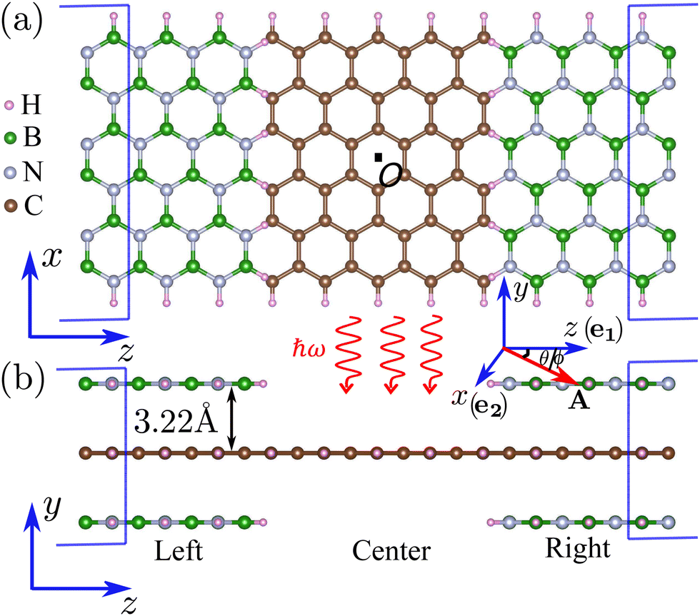 | ||
| Fig. 1 The transport junction with h-BN/graphene/h-BN vdW vertical heterostructure leads: (a) the top view and (b) the front view. It is divided into the left lead, the right lead and the channel region. In the leads, the ZGNR is sandwiched between two zigzag-edged h-BN nanoribbons. The sublattices of the h-BN nanoribbons in the left lead are exchanged with each other, compared with the sublattices of the right lead. Light is normally irradiated on the whole central region. A is the electromagnetic vector potential. e1 and e2 are two unit vectors for defining the polarization of the light, with the angle θ(ϕ) between e1 and A defined as the polarization/helicity angle. ħω is the photon energy. | ||
The calculation for the geometry relaxation is performed using density functional theory (DFT) with the Siesta code53 under the force tolerance control of 0.01 eV Å−1. Self-consistent two-probe calculations and subsequent photocurrent calculations are performed using Nanodcal,54 a package combining DFT and nonequilibrium Green's functions (NEGF) for quantum transport study. The atomic cores are described by norm-conserving pseudopotentials and the basis sets are taken as linear combinations of atomic orbitals in the form of double zeta plus polarization (DZP). The exchange–correlation potential is treated at the level of generalized gradient approximation (GGA), using the functional of Perdew, Burke, and Ernzerhof (PBE).55 The fineness of the real space grid is determined by an equivalent plane wave cutoff of 200 Ry. In this work, the spin–orbit coupling (SOC) effect is not considered since both atoms are light elements. The SOC effect will be important only in systems with heavy elements. For example, the SOC induced band gap in graphene is only 10−3 meV.56 Thus, neglecting SOC will not significantly change the band structure, density of states, and the subsequent optical properties.
The photocurrent from the central region to each lead is calculated in a postprocessing way. Firstly, the self-consistent Hamiltonians of the two leads and the central region are obtained by the DFT or DFT-NEGF formalism, without taking into account the electron–photon interaction at this stage. With these self-consistent Hamiltonians, the retarded (advanced) Green's function Gr0 (Ga0) of the central region without considering the electron–photon interaction is calculated. For simplicity of presentation, the spin index of all the quantities will be omitted temporarily. Then the electron–photon interaction is included in the calculation of the lesser (greater) Green's function of the central region by G<(>)ph = Gr0[Σ<(>)ph + Σ<(>)L + Σ<(>)R]Ga0, where Σr/aα is the self-energy of the semi-infinite lead α (α = (L, R)) and Σ</>ph is the self-energy from the electron–photon interaction considered in the first-order Born approximation.57 The effective transmission function is calculated as follows:18
| Teff,α(ε) = Tr{Γα(ε)[(1 − fα(ε))G<ph(ε) + fα(ε)G>ph(ε)]}, | (1) |
 | (2) |
 | (3) |
3. Results and discussion
First of all, we begin with the study of the electronic structures of the h-BN/graphene/h-BN vdW vertical heterostructure. In the ground state, the two edges of the single ZGNR are AFM coupled. The magnetic moment of edge carbon atoms at the two edges is 0.32μB and −0.32μB, respectively. Note that the band structure of the h-BN/graphene/h-BN vdW vertical heterostructure exhibits obvious spin-splitting (see Fig. 2(a) and (b)), which is induced by the stagger potential of the BN sheets.19 For the left lead, the band gap for spin up electrons is decreased to 0.30 eV while that for spin down electrons is increased to 0.78 eV, and the number 0.40 indicates the energy values. In contrast, the band gap for spin up electrons is increased to 0.78 eV while that for spin down electrons is decreased to 0.30 eV in the right lead. Fig. 2(c) shows the spin density of the ground state magnetic configurations of the single ZGNR, namely, AFM coupling between the two edges of the ZGNR. Importantly, the spin density exhibits spatial inversion antisymmetry, and O is the spatial inversion center. This spin density feature in the centrosymmetric h-BN/graphene/h-BN vdW vertical heterostructure suggests its great potential in the generation of pure spin current by the PGE.26 Thus, the pure spin current induced in the junction will be explored in the upcoming section. | ||
| Fig. 2 The band structure of the h-BN/graphene/h-BN vdW vertical heterostructure: (a) left lead, (b) zigzag graphene nanoribbon, and (c) right lead. The red and blue colors denote spin-up (UP) and spin-down (DN) channels, respectively. The numbers indicate the energy values. (d) The spin density of the transport junction, with O indicating the spatial inversion center. The red and blue colors indicate the atomic magnetic moments of spin up and spin down. | ||
Having understood the electronic structure of the junction with vdW vertical heterostructure leads, we now discuss the generation of a pure spin current in the system. The spin up (I↑), spin down (I↓) photocurrents, and the total charge photocurrents (Ic) as a function of photon energy under linearly polarized light with polarization angle θ = 0 are shown in Fig. 3(a). It is found that I↑, I↓ is nonzero when the photon energy ħω ≥ 0.54 eV, namely, the photon energy should be larger than the gap of the spin up Δ↑ and spin down component (Δ↑ = 0.38 + 0.16 = 0.54 eV, Δ↓ = 0.38 + 0.16 = 0.54 eV, see Fig. 2(a) and (b)), since below which electrons cannot be excited from the valence band to the conduction band due to spin mismatching, thus no photocurrent can be induced. Very interestingly, the generated photocurrents for the spin up and spin down components are equal in magnitude and opposite in direction, which indicates that the net charge current will always be zero according to Ic = I↑ + I↓ while the spin current Is = I↑ − I↓ is not. Thus, pure spin current is produced. Further investigation indicates that the pure spin current generated is so robust that it is sensitive neither to the polarization angle and nor to whether the light is linearly or elliptically polarized. Fig. 3(b and c) show the spin dependent photocurrents as a function of polarization or helicity angle under a linearly or elliptically polarized light with photon energy ħω = 0.70 eV slightly larger than the gap of Δ. It is clearly seen that both spin channels always have equal finite photocurrent with opposite signs. Therefore, pure spin current without accompanying charge current is generated and it is so robust that it is insensitive to the photon energy for ħω > Δ, its polarization angle and whether the light is linearly polarized or elliptically polarized.
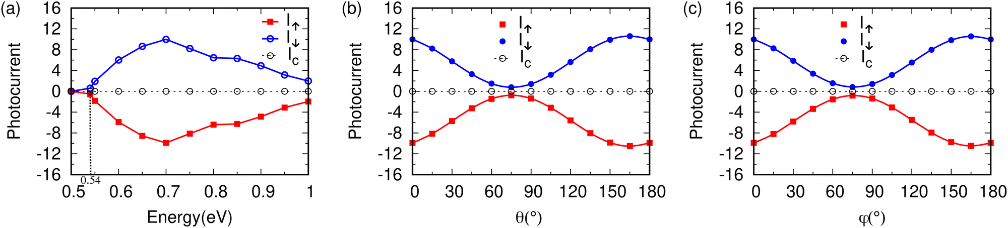 | ||
| Fig. 3 The spin-up I↑ and spin-down I↓ photocurrent, and total charge photocurrent Ic as a function of: (a) photon energy under LPL with a polarization angle θ = 0°; (b) polarization angle θ under LPL with photon energy ħω = 0.70 eV; (c) helicity angle ϕ under EPL with ħω = 0.70 eV. In the EPL case, ϕ = 45° and 135° mean right and left circularly polarized light, respectively. “I↑”, “I↓” and “Ic” mean the spin up, spin down and total charge photocurrent, respectively. | ||
To understand the physical process of pure spin current generation, the design principle of the pure spin current generated in our transport junction is illustrated in Fig. 4. The most striking feature of this system is that the band structure of the pristine ZGNR in the central region is spin degenerate while the two electrodes are spin-polarized. Moreover, two spin components in the two electrodes are exactly opposite (see Fig. 2), since the spin polarized transport is directly related to the spin resolved states of the system. We present the partial density of states (PDOS) of the left partial and the right partial of the transport junction as shown in Fig. 4(a) and (b). The energy and shape of the peaks in the left partial are the same as those in the right partial, while only the spin indices exchange. Based on these shape peaks (energy levels), the schematic diagram of the pure spin current generation is plotted in Fig. 4(c). Under light irradiation with photon energy ħω slightly larger than the spin gap Δ, the photon excites the valence electron to the conduction band. The spin down electrons at an energy level of “L1'' in the left are excited into the energy level of “R3” in the right and further move to the right lead due to spin matching. However, the same amount of spin up electrons at an energy level of “R1” in the right are excited into the energy level of “L3” in the left and further move to the left lead. Thus, the photocurrent with an opposite sign and equal magnitude is generated.
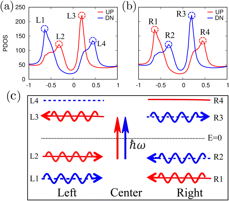 | ||
| Fig. 4 (a) The transport junction with vdW vertical heterostructure leads, while the central region is composed only of a zigzag graphene nanoribbon. (b) The process of pure spin current generation occurring between two spin subbands. v and c indicate the valence and conduction band while the red and blue lines are for the spin up and spin down channels, respectively. | ||
In the following, we will provide understanding of the physical mechanism of the generation of pure spin current by the PGE. The transport junction is symmetric with spatial inversion. The total charge density is also symmetric with spatial inversion, that is, ρ(r) = ρ(−r). Besides, ρ(r) is spin resolved for spin polarized systems, which means ρ(r) = ρ↑(r) + ρ↓(r). From Fig. 2(c), we know that the two spin dependent electron densities are anti-symmetric with spatial inversion, which means that after spatial inversion, the electron density of spin up(down) at point r has equal magnitude to that of the spin down(up) channel at point −r, that is, ρ↑(r) = ρ↓(−r) and ρ↓(r) = ρ↑(−r). Note that, the charge current is determined by total charge density, while the spin current is determined by the spin density. For our transport junction, the total charge density has spatial inversion symmetry, but that of each spin is symmetry breaking and meanwhile the spin density has spatial inversion anti-symmetry. Thus, the charge current (sum of the two spin channels) is zero while the spin current (difference of the two spin channels) is not. As a matter of fact, this is exactly the origin of zero charge current and finite pure spin current.
In order to further demonstrate the robustness of the generation of pure spin current by the PGE, we have considered several factors that may lead to the changes in the geometry structures. We mainly concern the effects of the vertical strain and the increase of h-BN nanoribbons layers on the pure spin current. To be specific, we have considered four cases: (1) an increase of the layer distance by 0.30 Å (+9.3%); (2) a decrease of the layer distance by 0.30 Å (−9.3%); (3) zigzag h-BN nanoribbons increased to four layers; (4) zigzag h-BN nanoribbons increased to six layers. We consider the first two cases since strain or pressure has become an important way to tune the properties and functions of a material or device design and we consider the last two cases since they may also appear in real situations. Since the generation of pure spin current is largely determined by spin splitting of the band structure, for qualitative discussions, it is enough to analyze the band structure change in these cases (see Fig. 5). It is seen that in all these cases, large spin splitting is always obtained. In particular, the change in the layer distance greatly affects the band structure. When it is decreased by 0.30 Å, the band gap for spin up is almost closed (0.06 eV) while that for spin down is increased to 0.86 Å (see Fig. 5(a)). Meanwhile, when the distance increased by 0.30 Å, the band gap is increased to 0.48 eV and 0.70 eV for spin up and spin down, respectively (see Fig. 5(b)). This is because the smaller the layer distance is, the larger the local potential difference between the CB and CN sublattices it will produce, which increases the energy difference of the edge states of different spins. For the case of increasing BN sheets on both sides of the graphene nanoribbons for the left and right leads, large spin splitting is still observed. Fig. 5(c) and (d) show the spin-splitting band structures with bilayer h-BN nanoribbons and trilayer h-BN nanoribbons distributed on both sides of the graphene nanoribbons, respectively. They show almost equal band gaps for each spin in the two cases (see Fig. 5(c) and (d), 0.28 and 0.28 eV for spin up while 0.79 and 0.78 eV for spin down). Therefore, pure spin current can always be achieved in all these cases, although the required photon energy range and the produced pure spin current magnitude may be different.
 | ||
| Fig. 5 The band structure for the cases where: (a) the layer distance is decreased by 0.30 Å; (b) the layer distance is increased by 0.30 Å; (c) bilayer h-BN nanoribbons distributed on both sides of graphene nanoribbons for the van der Waals heterostructure leads; (d) trilayer h-BN nanoribbons distributed on both sides of graphene nanoribbons for the van der Waals heterostructure leads. | ||
4. Conclusion
In summary, we have proposed a scheme of constructing zigzag edged graphene nanoribbon (ZGNR) transport junctions with h-BN/graphene/h-BN vdW vertical heterostructure leads for generating pure spin current with the photogalvanic effect (PGE). Since the structure of the device is symmetric and the spin density is anti-symmetric with respect to the inversion center, pure spin current without accompanying charge current can always be generated by the PGE. Importantly, the resulting pure spin current is not dependent on photon energy or the polarization/helicity angle, regardless of whether the light is linearly polarized or elliptically polarized. This scheme is quite robust because we always observe a large spin splitting, regardless of whether we decrease or increase the interlayer distance by applying compressive or tensile strain vertically to the leads. Finally, as the BN sheets on both sides of the graphene nanoribbons increase, large spin splitting is still observed and pure spin current can always be generated with the PGE in the vdW junctions. The findings highlight the significant role of h-BN/graphene/h-BN vdW vertical heterostructure in designing a ZGNR-based transport junction to generate a pure spin current and suggest the potential of using vdW heterostructures in designing spintronic devices based on two-dimensional materials.Data availability
The data that support the findings of this study are available from the corresponding author upon reasonable request.Conflicts of interest
There are no conflicts to declare.Acknowledgements
We gratefully acknowledge financial support by the National Natural Science Foundation of China under Grant No. 12104070, 12204202, 62074019, and 62174016 and the Natural Science Foundation of Jiangsu Province (Grant No. BK20210938 and BK20220679). We gratefully acknowledge HZWTECH for providing computation facilities.Notes and references
- Q. F. Sun and X. C. Xie, Phys. Rev. B, 2005, 72, 245305 CrossRef.
- J. E. Hirsch, Phys. Rev. Lett., 1999, 83, 1834–1837 CrossRef CAS.
- E. R. Mucciolo, C. Chamon and C. M. Marcus, Phys. Rev. Lett., 2002, 89, 146802 CrossRef PubMed.
- Q.-F. Sun, H. Guo and J. Wang, Phys. Rev. Lett., 2003, 90, 258301 CrossRef PubMed.
- J. Hübner, W. W. Rühle, M. Klude, D. Hommel, R. D. R. Bhat, J. E. Sipe and H. M. van Driel, Phys. Rev. Lett., 2003, 90, 216601 CrossRef PubMed.
- P. Jiang, X. X. Tao, H. Hao, L. L. Song, X. H. Zheng, L. Zhang and Z. Zeng, 2D Mater., 2017, 4, 035001 CrossRef.
- P. Jiang, X. X. Tao, L. L. Kang, H. Hao, L. L. Song, J. Lan, X. H. Zheng, L. Zhang and Z. Zeng, J. Phys. D: Appl. Phys., 2018, 52, 015303 CrossRef.
- Y. H. Zhou and X. H. Zheng, J. Condens. Matter Phys., 2019, 31, 315301 CrossRef CAS PubMed.
- Z. Ma, R. L. Wu, Y. B. Yu and M. Wang, J. Appl. Phys., 2014, 116, 043706 CrossRef.
- S. O. Valenzuela and M. Tinkham, Nature, 2006, 442, 176 CrossRef CAS PubMed.
- E. L. Ivchenko and G. E. Pikus, JETP Lett., 1978, 27, 604 Search PubMed.
- V. I. Belinicher, Phys. Lett. A, 1978, 66, 213 CrossRef.
- V. M. Asnin, A. A. Bakun, A. M. Danishevskii, E. L. Ivchenko, G. E. Pikus and A. A. Rogachev, JETP Lett., 1978, 28, 74 Search PubMed.
- Y. Yang, L. Zhang, X. Zheng, J. Chen, L. Xiao, S. Jia and L. Zhang, Phys. Chem. Chem. Phys., 2023, 25, 16363–16370 RSC.
- P. Jiang, X. Zheng, L. Kang, X. Tao, H.-M. Huang, X. Dong and Y.-L. Li, J. Mater. Chem. C, 2023, 11, 2703–2711 RSC.
- J. Chen, Y. Hu and H. Guo, Phys. Rev. B, 2012, 85, 155441 CrossRef.
- Y. Xie, L. Zhang, Y. Zhu, L. Liu and H. Guo, Nanotechnology, 2015, 26, 455202 CrossRef PubMed.
- L. Zhang, K. Gong, J. Chen, L. Liu, Y. Zhu, D. Xiao and H. Guo, Phys. Rev. B, 2014, 90, 195428 CrossRef.
- X. Tao, L. Zhang, X. Zheng, H. Hao, X. Wang, L. Song, Z. Zeng and H. Guo, Nanoscale, 2018, 10, 174–183 RSC.
- P. Zhao, J. Li, W. Wei, Q. Sun, H. Jin, B. Huang and Y. Dai, Phys. Chem. Chem. Phys., 2017, 19, 27233 RSC.
- F. Chu, M. Chen, Y. Wang, Y. Xie, B. Liu, Y. Yang, X. An and Y. Zhang, J. Mater. Chem. C, 2018, 6, 2509 RSC.
- J. Chen, L. Zhang, L. Zhang, X. Zheng, L. Xiao, S. Jia and J. Wang, Phys. Chem. Chem. Phys., 2018, 20, 26744–26751 RSC.
- P. Jiang, L. Kang, X. Tao, N. Cao, H. Hao, X. Zheng, L. Zhang and Z. Zeng, J. Phys.: Condens. Matter, 2019, 31, 495701 CrossRef CAS PubMed.
- Y. Xie, M. Chen, Z. Wu, Y. Hu, Y. Wang, J. Wang and H. Guo, Phys. Rev. Appl., 2018, 10, 034005 CrossRef CAS.
- H. Jin, J. Li, T. Wang and Y. Yu, Carbon, 2018, 137, 1–5 CrossRef CAS.
- X. Tao, P. Jiang, H. Hao, X. Zheng, L. Zhang and Z. Zeng, Phys. Rev. B, 2020, 102, 081402 CrossRef CAS.
- P. Jiang, X. Tao, H. Hao, Y. Liu, X. Zheng and Z. Zeng, npj Quantum Inf., 2021, 7, 21 CrossRef.
- L. Zhang, J. Chen, L. Zhang, F. Xu, L. Xiao and S. Jia, Carbon, 2021, 173, 565–571 CrossRef CAS.
- X. Tao, P. Jiang, Y. Dong, X. Yang, X. Zheng and Y. Liu, Phys. Chem. Chem. Phys., 2022, 24, 17131–17139 RSC.
- Z. Fu, P. Yan, J. Li, S. Zhang, C. He, T. Ouyang, C. Zhang, C. Tang and J. Zhong, Nanoscale, 2022, 14, 11316–11322 RSC.
- Y. Li, X. Shang, Y.-H. Zhou and X. Zheng, Phys. Chem. Chem. Phys., 2023, 25, 24428–24435 RSC.
- Y. Li, X. Shang, Y.-H. Zhou and X. Zheng, Phys. Chem. Chem. Phys., 2023, 25, 2890–2896 RSC.
- X. Shang, Y. Li, R. Cao, Y.-H. Zhou, W. Wan and X. Zheng, Opt. Express, 2023, 31, 36263–36272 CrossRef PubMed.
- L. Ponomarenko, A. Geim, A. Zhukov, R. Jalil, S. Morozov, K. Novoselov, I. Grigorieva, E. Hill, V. Cheianov and V. Fal'Ko, et al. , Nat. Phys., 2011, 7, 958–961 Search PubMed.
- L. Britnell, R. Gorbachev, R. Jalil, B. Belle, F. Schedin, A. Mishchenko, T. Georgiou, M. Katsnelson, L. Eaves and S. Morozov, et al. , Science, 2012, 335, 947–950 CrossRef CAS PubMed.
- C. R. Dean, A. F. Young, I. Meric, C. Lee, L. Wang, S. Sorgenfrei, K. Watanabe, T. Taniguchi, P. Kim and K. Shepard, et al. , Nat. Nanotechnol., 2010, 5, 722–726 CrossRef CAS PubMed.
- S. Haigh, A. Gholinia, R. Jalil, S. Romani, L. Britnell, D. Elias, K. Novoselov, L. Ponomarenko, A. Geim and R. Gorbachev, Nat. Mater., 2012, 11, 764–767 CrossRef CAS PubMed.
- Q. Li, M. Liu, Y. Zhang and Z. Liu, Small, 2016, 12, 32–50 CrossRef CAS PubMed.
- T. Georgiou, R. Jalil, B. D. Belle, L. Britnell, R. V. Gorbachev, S. V. Morozov, Y.-J. Kim, A. Gholinia, S. J. Haigh and O. Makarovsky, et al. , Nat. Nanotech., 2013, 8, 100–103 CrossRef CAS PubMed.
- A. K. Geim and I. V. Grigorieva, Nature, 2013, 499, 419–425 CrossRef CAS PubMed.
- Y. Liu, N. O. Weiss, X. Duan, H.-C. Cheng, Y. Huang and X. Duan, Nat. Rev. Mater., 2016, 16042 CrossRef CAS.
- S. Yang, L. Kang, X. Zheng, P. Jiang and G. Zhao, J. Chem. Phys., 2023, 159, 134702 CrossRef CAS PubMed.
- Y. Qiu, C.-S. Liu, X. Shi, X. Zheng and L. Zhang, Phys. Chem. Chem. Phys., 2023, 25, 25344–25352 RSC.
- H. Sadeghi, S. Sangtarash and C. J. Lambert, 2D Mater., 2017, 4, 015012 CrossRef.
- X. Tao, P. Jiang, L. Kang, H. Hao, L. Song, J. Lan, X. Zheng, L. Zhang and Z. Zeng, J. Phys. D: Appl. Phys., 2018, 51, 385301 CrossRef.
- K. Yasuda, X. Wang, K. Watanabe, T. Taniguchi and P. Jarillo-Herrero, Science, 2021, 372, 1458–1462 CrossRef CAS PubMed.
- A. Castellanos-Gomez, X. Duan, Z. Fei, H. R. Gutierrez, Y. Huang, X. Huang, J. Quereda, Q. Qian, E. Sutter and P. Sutter, Nat. Rev. Methods Primers, 2022, 2, 58 CrossRef CAS.
- X. Wu, X. Chen, R. Yang, J. Zhan, Y. Ren and K. Li, Small, 2022, 18, 2105877 CrossRef CAS PubMed.
- Y. Chen, C. Tan, Z. Wang, J. Miao, X. Ge, T. Zhao, K. Liao, H. Ge, Y. Wang and F. Wang, et al. , Sci. Adv., 2022, 8, eabq1781 CrossRef CAS PubMed.
- H. Wang, H. S. Wang, C. Ma, L. Chen, C. Jiang, C. Chen, X. Xie, A.-P. Li and X. Wang, Nat. Rev. Phys., 2021, 3, 791–802 CrossRef CAS.
- J. Qi, X. Qian, L. Qi, J. Feng, D. Shi and J. Li, Nano Lett., 2012, 12, 1224–1228 CrossRef CAS PubMed.
- J. Yu and W. Guo, J. Phys. Chem. Lett., 2013, 4, 951 CrossRef CAS PubMed.
- M. Brandbyge, J.-L. Mozos, P. Ordejón, J. Taylor and K. Stokbro, Phys. Rev. B, 2002, 65, 165401 CrossRef.
- J. Taylor, H. Guo and J. Wang, Phys. Rev. B, 2001, 63, 245407 CrossRef.
- J. P. Perdew, K. Burke and M. Ernzerhof, Phy. Rev. Lett., 1996, 77, 3865–3868 CrossRef CAS PubMed.
- Y. Yao, F. Ye, X.-L. Qi, S.-C. Zhang and Z. Fang, Phys. Rev. B, 2007, 75, 041401 CrossRef.
- L. E. Henrickson, J. Appl. Phys., 2002, 91, 6273–6281 CrossRef CAS.
| This journal is © the Owner Societies 2024 |