
 Open Access Article
 This Open Access Article is licensed under a
 Creative Commons Attribution 3.0 Unported Licence
Laser-induced tuning of crystallization in tetracene thin films
Andika
Asyuda
ab,
Johannes
Müller
a,
Mohammad Fardin
Gholami
a,
Anton
Zykov
a,
Linus
Pithan
c,
Christoph T.
Koch
 a,
Jürgen P.
Rabe
a,
Andreas
Opitz
*a and
Stefan
Kowarik
*d
a,
Jürgen P.
Rabe
a,
Andreas
Opitz
*a and
Stefan
Kowarik
*d
aInstitut für Physik & IRIS Adlershof, Humboldt-Universität zu Berlin, 12489 Berlin, Germany. E-mail: andreas.opitz@hu-berlin.de
bPhysik/Elektrotechnik: Institut für Mikrosensoren, -aktoren und -systeme, Universität Bremen, 28334 Bremen, Germany
cDeutsches Elektronen-Synchrotron (DESY), 22607 Hamburg, Germany
dPhysikalische Chemie, Universität Graz, 8010 Graz, Austria. E-mail: stefan.kowarik@uni-graz.at
First published on 12th September 2024
Abstract
This study explores how laser light affects the morphology of tetracene films, and it presents novel strategies for improving the creation of thin films used in (opto-)electronic devices. We demonstrate that laser light (532 nm, 1.1 W mm−2), applied during tetracene deposition, not only increases grain size but also induces photoalignment. The observed effects arise from enhanced molecular diffusion, resulting from energy transferred by light to the molecules after adsorption, but not from heating the substrate surface underneath. We observe that linearly polarized light promotes photoalignment, while increased crystallite sizes occurs with both linear and circular polarizations. We propose an Ostwald ripening process facilitated by laser illumination, where smaller crystallites get optically heated and dissolve, allowing molecules to surmount step-edge barriers and assemble into larger crystallites. Importantly, the crystallite sizes achieved with laser illumination surpass those attainable by substrate heating alone. The study demonstrates that laser illumination acts as a promising new parameter for controlling thin film properties and is distinct from growth control via substrate temperature and growth rate. Light control also includes the ability for lateral patterning, with implications for the future of molecular materials and their manufacturing technologies.
Introduction
Nucleation and crystal growth are foundational processes in the formation of crystalline materials with a wide range of applications. For tetracene, this includes nanoparticles for photocatalysis1 or semiconductor thin films used in electronics2–4 and optoelectronics.5–10 Although it is a critical step in the growth of these materials, many aspects of nucleation remain poorly understood. Questions persist about the nature of aggregates before nucleation, the existence and role of amorphous precursor phases, and the methods available to externally control the nucleation process.Laser illumination has been identified as a method with the potential to influence 3D nucleation and crystalisation.11 The technique, known as non-photochemical laser-induced nucleation (NPLIN),12,13 is gaining attention for its ability to control nucleation both spatially and temporally through the manipulation of the laser's spot size and its duration of application. Separate from NPLIN as a method for bulk crystallisation, laser illumination has also proven useful in thin film growth. For instance, for growth of organic semiconductor materials such as sexithiophene (6T), controlled laser illumination has been leveraged for selecting specific polymorphic forms and thereby influencing electrical and optical properties.14 Similarly, during growth of tetracene thin films, the direction of laser polarization has been found to influence crystal alignment, demonstrating that laser illumination is a promising way to control nucleation and thin film growth.15 However, until now, the discussion on NPLIN has primarily focused on bulk crystal growth from solutions or melts, not extending to vacuum-deposited thin films. Mechanisms such as bubble formation are specific to NPLIN from solution and the effects of laser illumination during organic molecular beam deposition have not yet been studied extensively. Also, NPLIN usually is using high peak power, pulsed lasers, whereas our work employs comparatively low power continuous wave lasers. While our previous work14,15 has established the fact that laser illumination affects crystal phase and crystal orientation in organic molecular beam deposition, crucial information regarding light-induced effects on nucleation densities, crystallite sizes, and the thin film roughness remains lacking.
In this study we demonstrate how laser illumination during tetracene thin film growth can induce the formation of larger crystallites, significantly altering the morphology of thin films. The observed effects are not a consequence of mere laser-induced substrate heating but are attributed to light-matter interactions within the growing tetracene thin film. Larger crystallite sizes and enhanced photoluminescence (PL) are noted under both linear and circularly polarized laser light. However, photoalignment is uniquely observed with linear polarization, underscoring the nuanced control that laser parameters offer in the thin film nucleation process. This study can also be seen as a first example that expands the concepts of NPLIN to the domain of thin films grown in vacuum, further establishing laser light as a novel lever to control crystallisation and film growth.
Experimental methods
Thin film growth
Tetracene powder was purchased from Sigma Aldrich and used without a further purification. It was placed into the crucible of an effusion cell. Outgassed glass wool was inserted afterwards to hold the tetracene powder in place for top-down evaporation. Silicon substrates measuring approximately 10 × 10 mm2 and featuring a 200 nm oxide layer were sequentially sonicated for 5 minutes each in acetone, followed by distilled water, and concluding with isopropanol to ensure a clean surface for thin film deposition. Then, substrates were immediately dried using a nitrogen gun, and stored in the organic molecular beam deposition (OMBD) vacuum chamber with a base pressure below 5 × 10⁻⁷ mbar. Substrates were mounted with silver conductive paint onto a molybdenum sample holder with resistive heating and cryogenic nitrogen cooling. The temperature measurements and temperature stabilisation were performed with a K-type thermocouple attached to the molybdenum sample holder. Through comparisons between the sample holder thermocouple and thermocouples in direct contact with the silicon wafer, we estimate our absolute temperature error to be below 10 K. However, the reproducibility and relative accuracy of temperature measurements within the same setup are significantly higher, with an estimated precision of 1 K. Before film growth, substrates were heated at 100 °C overnight, and then at 200 °C for 1 hour. The nominal film thickness of deposited tetracene was controlled via a quartz crystal microbalance (QCM) and kept constant at 30 nm. The same molecular flux of 1 nm min−1 was used for all films.The setup for tetracene film growth under laser illumination is illustrated schematically in Fig. 1a. During the deposition process, selected substrates were subjected to laser illumination at 1.5 W power to assess the effects of illumination on thin film growth. A 532 nm wavelength diode pumped solid state (DPSS) laser from Roithner Lasertechnik was used. The 532 nm wavelength aligns with the first Davydov component of tetracene crystallite absorption, resulting in strong and directional light absorption. The laser spot size at the sample had a full width at half maximum (FWHM) of 0.64 mm. For several films we converted the laser light from linear to circular polarization by placing a quarter-wave plate in the laser beam path before it entered the vacuum chamber glass window. The temperature of the sample holder during the film growth was kept at a constant value using a PID controlled heating element and constant liquid nitrogen flow for cooling.
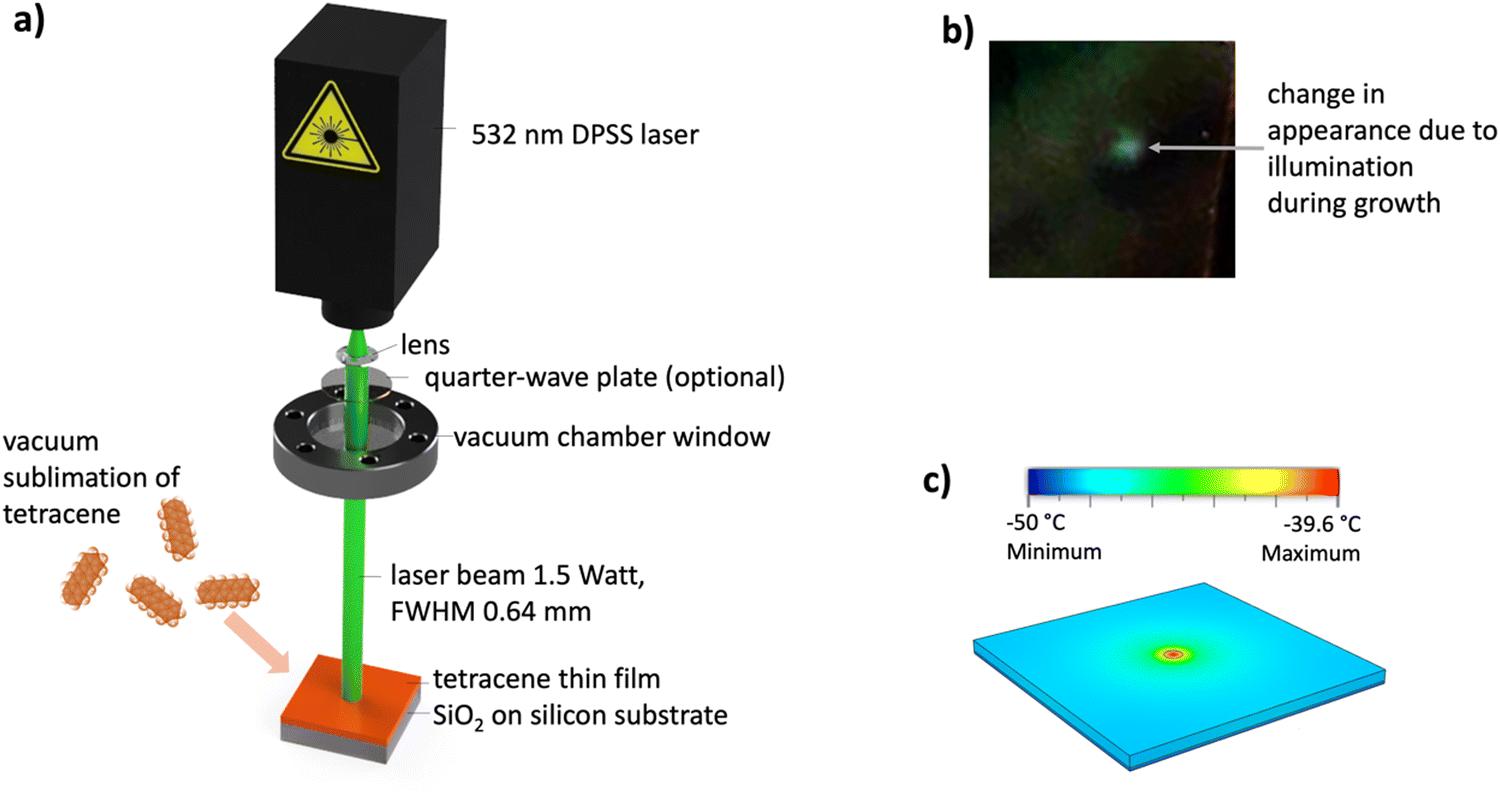 | ||
| Fig. 1 (a) Schematic of the setup for tetracene growth involving laser illumination. (b) Photograph in natural light of a ca 10 mm × 10 mm tetracene sample, which was grown under laser illumination, exhibiting a spot of ≈1 mm with changed appearance, where the laser hit. (c) Heat-flow simulation of the substrate heating through the laser demonstrates a ≈11 °C rise in substrate temperature in the illuminated spot. | ||
Photoluminescence (PL)
To gain insight into PL of tetracene films with and without laser illumination during growth, we employed a polarization-dependent PL setup. Tetracene samples were excited using a 455 nm LED from Thorlabs. Tetracene emission was collected by a lens, then passed through a polarizer, a long pass filter, and an optical fibre into the compact CCD spectrometer CCS200 from Thorlabs. Background signal and sample luminescence were both recorded for 19 seconds for each measurement at room temperature. The dependence of integrated PL counts in the range 2.3–2.5 eV on the angular position of polarizer was used to calculate a dichroic ratio.Atomic force microscopy (AFM)
The surface morphology of tetracene films was determined using a Bruker Nanoscope V multimode 8 AFM with ScanAsyst mode and OTESPA-R3 tip (spring constant 26 N m−1). AFM data were analysed with the open source software Gwyddion to obtain roughness, grain height and grain area.16Scanning electron microscope (SEM)
We used a Zeiss GeminiSEM 500 to image the samples from the top and in cross section in order to obtain the lateral grain size and the grain thickness, respectively. The SEM was operated at an acceleration voltage of 10 kV with the 20 μm aperture and the in-lens detector was used to acquire the images. For the cross-sectional SEM, the angle between sample surface and incoming electron beam was 5°. For SEM cross sections, samples were prepared by breaking the silicon substrate across the visible illumination position (see Fig. 1b). SEM images were analysed with the software Fiji.Results
Our study investigates the impact of laser illumination on the nucleation and growth of crystalline tetracene thin films. We use a comparative approach, analysing samples prepared under varying substrate temperatures and different illumination conditions. A crucial aspect is the role of trivial laser-induced substrate heating versus optical growth control by direct light absorption in the molecular layer. For this we explore morphological changes of the tetracene thin film, photoalignment of crystallites and larger crystallite sizes with enhanced photoluminescence. These changes clearly show that optical growth control goes beyond substrate heating and molecular flux control.To estimate the direct heating effects of the laser on the substrate we use finite element simulations. These simulations, one of which is depicted in Fig. 1c, confirm that a localized temperature rise is limited to about 11 K. The simulation provides the steady-state temperature distribution between a laser-heated circle with a 0.64 mm diameter at the top of the substrate, with a power density of approximately 1.1 W mm−2, and a heat sink maintained at −50 °C at the base of the glue layer. The simulations were conducted using Autodesk Fusion 360, which modelled heat flow through a silicon wafer with a thickness of 0.4 mm and a thermal conductivity of 150 W m−1 K−1, and an epoxy glue layer with a thickness of 0.1 mm and a thermal conductivity of 0.46 W m−1 K−1. The absorbed power from the laser beam, adjusted for the silicon reflectivity, was set at 0.94 W. For two backside temperatures of −50 °C and −25 °C at the sample holder, which is where the thermocouple is positioned in the experiment, the temperature increment remained below 11 K. Notably, the area of a 5 K temperature rise is a wide spot of ca. 4 mm diameter, whereas the grown tetracene film shows a narrower ca. 1 mm diameter spot with changed, milky appearance only where the laser hit (see Fig. 1b). This is a first indication that this minor, localized substrate heating cannot be the sole factor in the morphological changes observed. Note that the demarcation of non-illuminated areas and the central laser illuminated spot enables a direct comparison between the illuminated and non-illuminated film regions on the same substrate in further experiments. While it would be interesting to perform a similar calculation of the temperature within the tetracene film to understand the direct optical effects better, too little is known about heat transfer within tetracene and across tetracene-silica interfaces to arrive at a reasonably accurate estimate.
To contextualize these findings of a roughly 11 K rise due to thermal effects of the laser illumination on the Si-substrate we performed a temperature dependent growth study of tetracene growth without illumination. A wide 70 K range of different substrate temperatures was investigated with samples grown at −50 °C, −25 °C, and 20 °C in line with previous, temperature-dependent growth studies.17–19 The upper limit of 20 °C, was established based on the volatility of tetracene molecules at our specific growth rate, which precludes higher temperature growth due to molecular desorption. Note that slightly higher substrate temperatures of 30 °C in literature were possible, but only when using significantly higher deposition rates.19 The respective AFM micrographs without laser illumination are shown in Fig. 2a–c. As expected, the nucleation density decreases for higher temperatures as tetracene molecules become more mobile and can diffuse to nucleation sites in the vicinity rather than nucleating a new island. Because of the lower nucleation density, the grain size increases correspondingly with temperature.19,20 We expect the film to consist of the tetracene thin film phase,21,22 however the details of tetracene polymorphism are not the focus of this study.
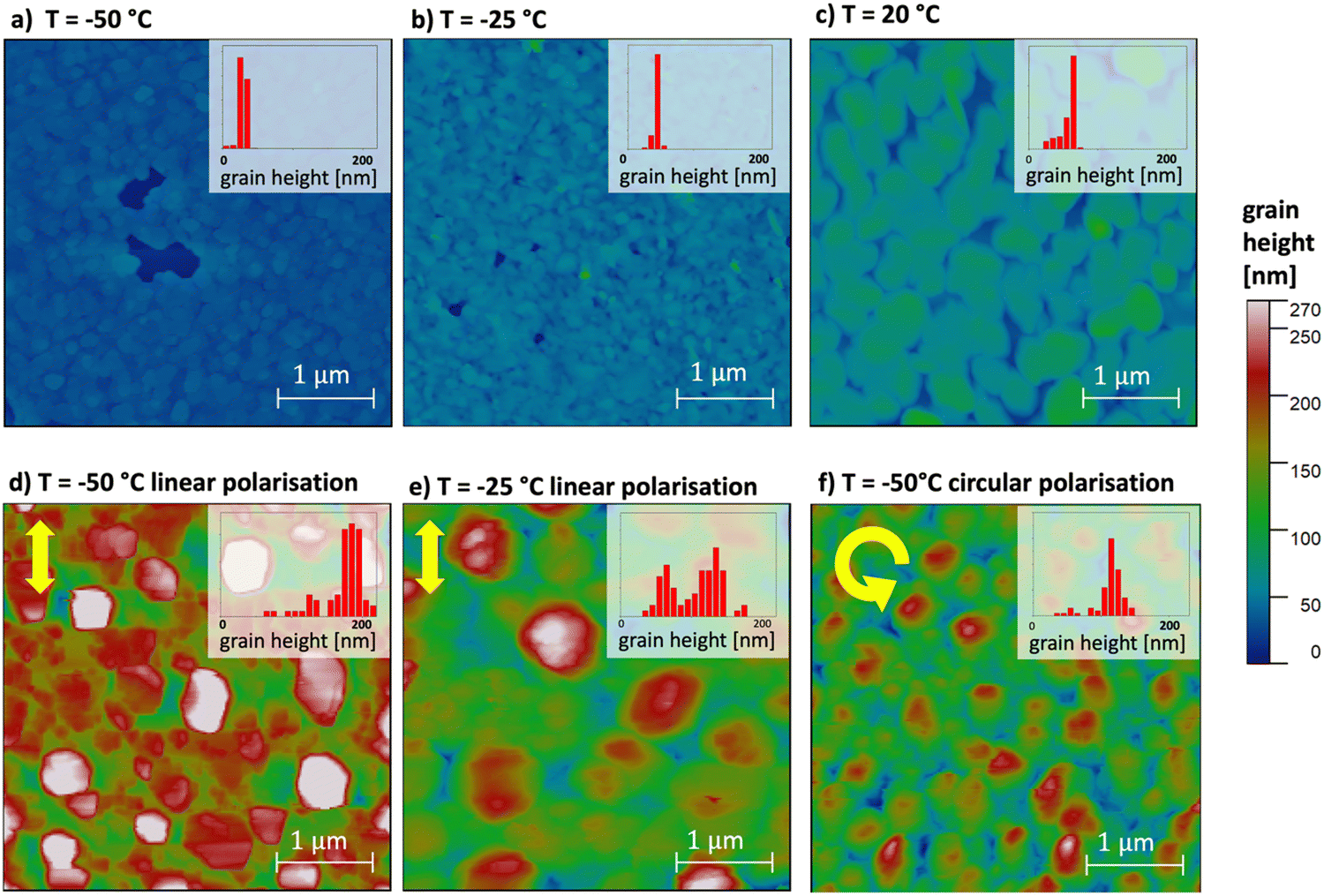 | ||
| Fig. 2 AFM micrographs of tetracene film (size 4 × 4 μm2), grown on SiO2 substrate without illumination in the top (a)–(c) and with laser illumination (LP and CP) in the bottom (d)–(f). The insets show the height histograms for the micrographs. The height and width of crystallites increases significantly under illumination. | ||
Fig. 2 panels (d)–(f) showcase the surface morphology of tetracene films grown under linearly polarized (LP) and circularly polarized (CP) laser illumination. For both LP and CP conditions during the growth phase, an increase in grain size is evident when compared to films grown without any form of illumination at equivalent temperatures. This is quantitatively detailed in Table 1, where lateral grain size, vertical grain height—as depicted in the histogram insets of the figure—and surface roughness, all measured from atomic force microscopy (AFM) images, exhibit a consistent upward trend with the introduction of illumination. The modest temperature elevation of 11 K as calculated for the laser substrate heating above cannot account for the observed augmentation in grain size. The analysis becomes even more compelling when considering that films grown without illumination at a substrate temperature of −25 °C possess grains that are markedly smaller than those in films grown under illuminated conditions at a colder −50 °C sample holder temperature, which we calculate to be −39 °C in the laser spot. Even when comparing the laser assisted growth at −39 °C/−50 °C to the dark growth at the highest substrate temperature of 20 °C, the grain size achieved under illuminated conditions is still larger. These observations underscore the role of illumination as a novel control variable in OMBD to adjust grain size.
| Growth conditions | No laser −50 °C | LP −50 °C | CP −50 °C | No laser −25 °C | LP −25 °C | No laser 20 °C |
|---|---|---|---|---|---|---|
| Lateral grain size [μm2] | 0.037 | 0.226 | 0.269 | 0.054 | 0.532 | 0.186 |
| Grain height [nm] | 29 | 171 | 112 | 44 | 105 | 62 |
| Roughness [nm] | 4 | 37 | 32 | 5 | 33 | 11 |
| Dichroic ratio (measure of crystalline alignment) | 9% | 54% | 4% | 6% | 56% | 7% |
Fig. 3 presents the SEM results that echo the AFM findings, highlighting increases in the tetracene film grain height and diameter in response to linear-polarized laser light exposure during growth. In contrast to the AFM images which are each taken on a different sample, the SEM measurements provide information on the lateral changes on spots with/without laser illumination on the same sample. These variations, summarised in Fig. 3e together with the laser intensity profile, confirm the influence of laser light on the film morphology, with grain dimensions expanding notably at the centre of the laser spot. It is noteworthy, that the FWHM of the grain height (0.70 ± 0.17) mm aligns closely with the actual laser spot FWHM (0.64 ± 0.17) mm, both deduced from Gaussian fits, suggesting a correlation with the growth process of tetracene within the vacuum chamber. Conversely, the grain diameter shows a broader distribution (1.19 ± 0.22) mm, slightly exceeding the span of the laser beam. This can be rationalised by the fact that lateral diffusion has a lower energy barrier than vertical diffusion across step edges. Therefore, hot adsorbate molecules can diffuse out of the laser spot maximum.
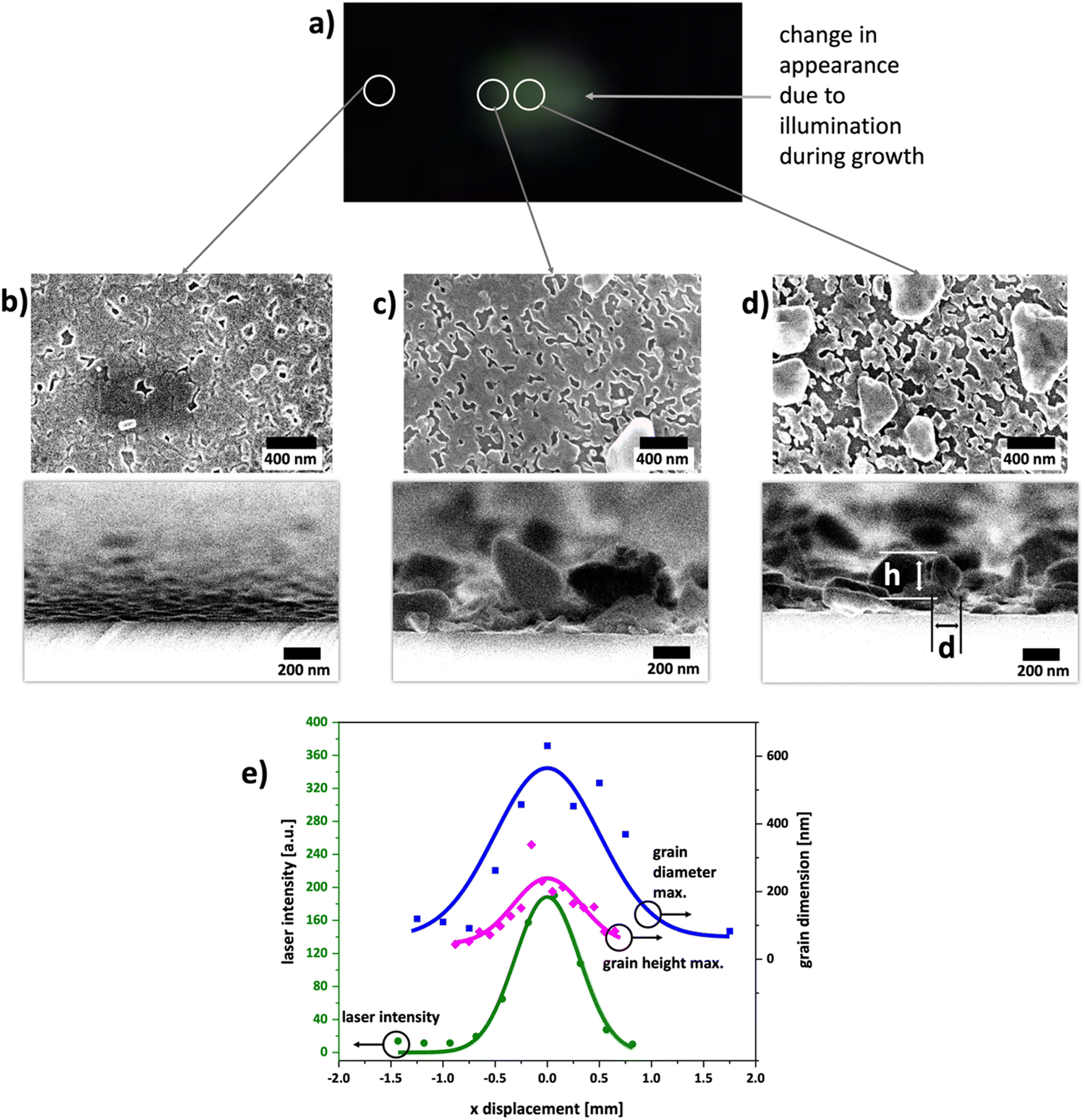 | ||
| Fig. 3 (a) Photograph of a sample which was grown at substrate temperature −50 °C and molecular flux 1 nm min−1. Up to a thickness of 30 nm, while a linear-polarized laser light was applied in the centre of the sample. Top-view and cross-section SEM images of the tetracene film grown in a region without illumination (b), at the edge of the illuminated region (c), and close to the centre of the laser spot (d). In (e) the grain height and grain diameter extracted from SEM images as well as the laser intensity profile are plotted as a function of the lateral sample position. For the combined plot, the maximum of the laser intensity profile was aligned on the x-axis to match the maximum of the grain parameters. | ||
Consistent with findings in ref. 15 our study reveals photoalignment in tetracene crystals formed under linearly polarized (LP) laser illumination, a phenomenon consistent across various substrate temperatures. Photoluminescence (PL) was observed for all films, and the presence of facets on the crystalline grains suggests that the films comprise crystallites rather than amorphous structures. Within these crystals, the orientation of tetracene molecules is predominantly vertical, allowing for efficient absorption and emission of light perpendicular to the substrate.23 Our analysis, detailed in Table 1, shows a dichroic ratio exceeding 54%, which, while significant, is less than that reported by Pithan et al.15 This discrepancy can be attributed to the higher molecular flux of 1 nm min−1 used in our experiments, which shortens the deposition time and thus, the window for interaction between the laser light and the growing crystallites. Films grown in the absence of laser illumination, or under circularly polarized (CP) light, demonstrate minimal dichroic ratios between 4% and 9%. These ratios fall within the uncertainty margin of our apparatus, suggesting that these films do not display notable dichroism. The inclusion of a quarter waveplate in the experimental setup resulted in a negligible reduction in laser power from 1.5 W to 1.4 W, insufficient to account for the dichroic ratio plummeting to 4% under CP laser light. This further underscores the crucial influence of laser polarization in fostering the growth of orientationally aligned tetracene crystals. Ultimately, the observed photoalignment serves as another proof of the direct interaction of light with the crystalline structure of the thin film, distinct from any thermal substrate heating effects that might arise but could not result in crystal alignment on an amorphous substrate.
In Fig. 4a, we observe that tetracene films grown under circularly polarized laser light at a substrate temperature of −50 °C show a significant increase in PL intensity in the illuminated areas, with a roughly twofold enhancement compared to the non-illuminated regions. This enhancement is consistent with the larger grain sizes induced by laser illumination, and may be a sign of superradiance in larger, better ordered and bulk-like crystals.24–26 This enhanced molecular ordering within the crystal structure is also evidenced by the clearer Davydov component, seen as a shoulder at ca. 2.2 eV.27 This observation of increased PL is consistently found also for other laser illuminated samples, though the exact enhancement factor varies. In Fig. 4b, polarised PL is shown as a function of the azimuthal angle of the polarizer in the detection path. The PL is clearly weaker for films grown in the dark. Strong azimuthal alignment and polarized PL is only found for LP laser illumination, while CP and dark films show little to no azimuthal dependency of the PL. These findings showcase the role of laser illumination in dictating the growth and subsequently also the photophysical behaviour of tetracene thin films.
 | ||
| Fig. 4 (a) Photoluminescence (PL) of a tetracene film grown at a substrate temperature −50 °C under circular-polarized laser light. The excitation power is 2.5 mW. A twofold enhancement of the PL intensity of tetracene is found at the position illuminated during growth with respect to the position not illuminated during growth at the side of the sample. (b) Azimuthal, polarization dependent PL intensity distribution for different illumination conditions during growth. An enhancement of the PL is observed under any laser illumination but photoalignment of crystallites only for linearly polarised laser illumination. | ||
Discussion
The role of laser illumination in the growth of crystals has been a subject of keen interest due to its unique influences on material properties. In our investigation of laser control in molecular beam deposition, we discern that laser illumination distinctly differs from a mere increase in substrate temperature. Typically, an elevated substrate temperature can cause impinging molecules to desorb immediately, a phenomenon that can hinder or completely prevent controlled thin film growth. In contrast, we propose direct laser heating of the molecular film occurs in a three-step process: (i) initial adsorption and thermalisation of hot adsorbed molecules on the cold substrate, (ii) formation of a tetracene nucleus, (iii) absorption of the light in the nucleus leading to an increase in the temperature and kinetic energy of the molecules. This technique maintains the molecules in their adsorbed state before energy is optically applied, leading to more controlled growth without desorption.Most studies on non-photochemical laser-induced nucleation (NPLIN) use laser wavelengths outside the target compound's absorption bands to avoid photochemical effects. Although single tetracene molecules exhibit no absorption for photons at 532 nm, the crystals are expected to strongly absorb at this wavelength. Still, in the vacuum environment of our experiments, stable tetracene molecules show no significant photochemical effects, affirming that we are examining a purely non-photochemical process. Tetracene crystals absorb light at 532 nm, but individual molecules do not. This indicates that the effects we observed happen after nucleation. A high nucleation density is presumed to initiate the process, but the subsequent laser-induced heating of the small crystallites may trigger their dissolution, potentially causing a process akin to Ostwald ripening.28 This would result in the growth of larger crystallites at the expense of smaller ones. Larger crystals possess a reduced surface-to-volume ratio, diminishing the probability of molecules detaching from the surface under the influence of illumination during growth. Moreover, larger crystals with their extensive molecular networks exhibit more pronounced thermalization processes, which can mitigate the loss of molecules, in contrast to smaller nuclei, which lack such extensive interactions and are more susceptible to dissolution. The presence of this effect under both linear and circular laser polarizations leads us to conclude that photoalignment and the increase in crystallite size are independent phenomena.
Notably, during the growth influenced by linearly polarized (LP) light, we observe that the efficiency of tetracene crystal dissolution is contingent upon the angle between the crystal's transition dipole moment and the laser polarization. For LP laser-assisted growth, the alignment of tetracene aggregates is enhanced, again suggesting an Ostwald ripening-like mechanism. The directional dependency supports the idea that orientationally selective energy transfer and a resulting orientation dependent temperature contributes to the growth of aligned crystals.
To further support our findings, the microscopy results from both SEM and AFM point towards an enhancement of tetracene molecule diffusion, both laterally across the substrate surface, and vertically along pre-existing tetracene grains, indicating an upward transport mechanism. This kind of transport during film growth aligns with the observations reported by Nahm et al.,19 where it was found that increasing the temperature facilitates overcoming the step-edge barrier for upward diffusion of molecules. Our results corroborate this phenomenon, as we observe that under laser illumination and optical heating the vertical crystallite size increases beyond the effect possible through increased substrate temperature. Laser illumination greatly promotes the vertical transport and assembly of tetracene molecules into taller crystalline structures.
Conclusion & outlook
Our investigation establishes that laser illumination significantly influences the growth of tetracene thin films, enhancing grain size and promoting photoalignment due to the diffusion enhancement of tetracene molecules. This is attributed to optical energy transfer mechanisms after the hot adsorbed molecules have thermalised on the cold substrate, and laser control of growth is distinct from the standard growth control parameters of substrate temperature and growth rate. The ability to modulate thin film properties through laser parameters including polarisation, wavelength, and power density along with the capability to create lateral structures with patterned light, suggests a pathway to tailored material functionalities. This technique is especially valuable in the field of organic electronics, where exact control over film morphology is crucial.Future research will benefit from a deeper exploration into the theoretical aspects of energy transfer during film growth and broadening the scope to include diverse materials and laser conditions. This advancement in laser-assisted deposition techniques promises to refine our approach to thin film growth, paving the way for enhanced and versatile structure–function relationships in molecular materials.
Data availability
The data that support the findings of this study are available on request from the corresponding author, Stefan Kowarik.Conflicts of interest
There are no conflicts to declare.Acknowledgements
We thank Dr Nikolai Severin, Dr Valentin Reiter-Scherer, Dr Paul Beyer, Dr Rongbin Wang, Prof. Xiaomin Xu, and Dr Qiankun Wang for assistance with the OMBD system and AFM. JPR and MFG acknowledge the support of the Cluster of Excellence “Matters of Activity. Image Space Material” funded by the Deutsche Forschungsgemeinschaft (DFG, German Research Foundation) under Germany's Excellence Strategy – EXC 2025 – 390648296. AA would like to acknowledge the DAAD-ACEH Scholarship of Excellence from the German Academic Exchange Service.References
- H. Y. Kim, T. G. Bjorklund, S.-H. Lim and C. J. Bardeen, Spectroscopic and Photocatalytic Properties of Organic Tetracene Nanoparticles in Aqueous Solution, Langmuir, 2003, 19, 3941–3946 CrossRef CAS.
- R. W. I. de Boer, T. M. Klapwijk and A. F. Morpurgo, Field-effect transistors on tetracene single crystals, Appl. Phys. Lett., 2003, 83, 4345–4347 CrossRef CAS.
- J. Shi, D.-T. Jiang, J. R. Dutcher and X.-R. Qin, Thickness-dependent mobility in tetracene thin-film field-effect-transistors, J. Vacuum Sci. Technol. B, 2015, 33, 050604 CrossRef.
- F. Cicoira, C. Santato, F. Dinelli, M. Murgia, M. A. Loi, F. Biscarini, R. Zamboni, P. Heremans and M. Muccini, Morphology and Field-Effect-Transistor Mobility in Tetracene Thin Films, Adv. Funct. Mater., 2005, 15, 375–380 CrossRef CAS.
- T. Takahashi, T. Takenobu, J. Takeya and Y. Iwasa, Ambipolar Light-Emitting Transistors of a Tetracene Single Crystal, Adv. Funct. Mater., 2007, 17, 1623–1628 CrossRef CAS.
- T. C. Wu, N. J. Thompson, D. N. Congreve, E. Hontz, S. R. Yost, T. Van Voorhis and M. A. Baldo, Singlet fission efficiency in tetracene-based organic solar cells, Appl. Phys. Lett., 2014, 104, 193901 CrossRef.
- N. J. Thompson, M. W. B. Wilson, D. N. Congreve, P. R. Brown, J. M. Scherer, T. S. Bischof, M. Wu, N. Geva, M. Welborn, T. V. Voorhis, V. Bulović, M. G. Bawendi and M. A. Baldo, Energy harvesting of non-emissive triplet excitons in tetracene by emissive PbS nanocrystals, Nat. Mater., 2014, 13, 1039–1043 CrossRef CAS.
- P. J. Jadhav, A. Mohanty, J. Sussman, J. Lee and M. A. Baldo, Singlet Exciton Fission in Nanostructured Organic Solar Cells, Nano Lett., 2011, 11, 1495–1498 CrossRef CAS PubMed.
- R. W. MacQueen, M. Liebhaber, J. Niederhausen, M. Mews, C. Gersmann, S. Jäckle, K. Jäger, M. J. Y. Tayebjee, T. W. Schmidt, B. Rech and K. Lips, Crystalline silicon solar cells with tetracene interlayers: the path to silicon-singlet fission heterojunction devices, Mater. Horiz., 2018, 5, 1065–1075 RSC.
- J. Niederhausen, R. W. MacQueen, E. Özkol, C. Gersmann, M. H. Futscher, M. Liebhaber, D. Friedrich, M. Borgwardt, K. A. Mazzio, P. Amsalem, M. H. Nguyen, B. Daiber, M. Mews, J. Rappich, F. Ruske, R. Eichberger, B. Ehrler and K. Lips, Energy-Level Alignment Tuning at Tetracene/c-Si Interfaces, J. Phys. Chem. C, 2020, 124, 27867–27881 CrossRef CAS.
- Y. Liu, M. H. van den Berg and A. J. Alexander, Supersaturation dependence of glycine polymorphism using laser-induced nucleation, sonocrystallization and nucleation by mechanical shock, Phys. Chem. Chem. Phys., 2017, 19, 19386–19392 RSC.
- A. J. Alexander and P. J. Camp, Non-photochemical laser-induced nucleation, J. Chem. Phys., 2019, 150, 040901 CrossRef PubMed.
- A. Ikni, B. Clair, P. Scouflaire, S. Veesler, J.-M. Gillet, N. El Hassan, F. Dumas and A. Spasojević-de Biré, Experimental Demonstration of the Carbamazepine Crystallization from Non-photochemical Laser-Induced Nucleation in Acetonitrile and Methanol, Cryst. Growth Des., 2014, 14, 3286–3299 CrossRef CAS.
- L. Pithan, C. Cocchi, H. Zschiesche, C. Weber, A. Zykov, S. Bommel, S. J. Leake, P. Schäfer, C. Draxl and S. Kowarik, Light controls polymorphism in thin films of sexithiophene, Crystal Growth Design, 2015, 15, 1319–1324 CrossRef CAS.
- L. Pithan, P. Beyer, L. Bogula, A. Zykov, P. Schäfer, J. Rawle, C. Nicklin, A. Opitz and S. Kowarik, Direct Photoalignment and Optical Patterning of Molecular Thin Films, Adv. Mater., 2017, 29, 1604382 CrossRef PubMed.
- D. Nečas and P. Klapetek, Gwyddion: an open-source software for SPM data analysis, Open Phys., 2012, 10, 181–188 CrossRef.
- R. K. Nahm and J. R. Engstrom, Who's on first? Tracking in real time the growth of multiple crystalline phases of an organic semiconductor: Tetracene on SiO2, J. Chem. Phys., 2016, 146, 052815 CrossRef.
- R. K. Nahm and J. R. Engstrom, Unexpected Effects of the Rate of Deposition on the Mode of Growth and Morphology of Thin Films of Tetracene Grown on SiO2, J. Phys. Chem. C, 2016, 120, 7183–7191 CrossRef CAS.
- R. K. Nahm, H. J. Bullen, T. Suh and J. R. Engstrom, Faster Is Smoother and So Is Lower Temperature: The Curious Case of Thin Film Growth of Tetracene on SiO2, J. Phys. Chem. C, 2017, 121, 8464–8472 CrossRef CAS.
- J. Shi and X. R. Qin, Nucleation and growth of tetracene films on silicon oxide, Phys. Rev. B: Condens. Matter Mater. Phys., 2008, 78, 115412 CrossRef.
- L. Pithan, D. Nabok, C. Cocchi, P. Beyer, G. Duva, J. Simbrunner, J. Rawle, C. Nicklin, P. Schäfer, C. Draxl, F. Schreiber and S. Kowarik, Molecular structure of the substrate-induced thin-film phase of tetracene, J. Chem. Phys., 2018, 149, 144701 CrossRef PubMed.
- J. Niederhausen, R. W. MacQueen, K. Lips, H. Aldahhak, W. G. Schmidt and U. Gerstmann, Tetracene Ultrathin Film Growth on Hydrogen-Passivated Silicon, Langmuir, 2020, 36, 9099–9113 CrossRef CAS PubMed.
- S. Tavazzi, L. Raimondo, L. Silvestri, P. Spearman, A. Camposeo, M. Polo and D. Pisignano, Dielectric tensor of tetracene single crystals: The effect of anisotropy on polarized absorption and emission spectra, J. Chem. Phys., 2008, 128, 154709 CrossRef CAS.
- S.-H. Lim, T. G. Bjorklund, F. C. Spano and C. J. Bardeen, Exciton Delocalization and Superradiance in Tetracene Thin Films and Nanoaggregates, Phys. Rev. Lett., 2004, 92, 107402 CrossRef PubMed.
- J. J. Burdett, A. M. Müller, D. Gosztola and C. J. Bardeen, Excited state dynamics in solid and monomeric tetracene: The roles of superradiance and exciton fission, J. Chem. Phys., 2010, 133, 144506 CrossRef PubMed.
- J. J. Burdett and C. J. Bardeen, The Dynamics of Singlet Fission in Crystalline Tetracene and Covalent Analogs, Acc. Chem. Res., 2013, 46, 1312–1320 CrossRef CAS PubMed.
- G. B. Piland and C. J. Bardeen, How Morphology Affects Singlet Fission in Crystalline Tetracene, J. Phys. Chem. Lett., 2015, 6, 1841–1846 CrossRef CAS.
- S. Mahesh, A. Gopal, R. Thirumalai and A. Ajayaghosh, Light-Induced Ostwald Ripening of Organic Nanodots to Rods, J. Am. Chem. Soc., 2012, 134, 7227–7230 CrossRef CAS PubMed.
| This journal is © the Owner Societies 2024 |