
 Open Access Article
 This Open Access Article is licensed under a
 Creative Commons Attribution 3.0 Unported Licence
Mechanism of charge accumulation in potassium poly(heptazine imide)†
Goichiro
Seo
 *a,
Ryoma
Hayakawa
b,
Yutaka
Wakayama
b,
Ryosuke
Ohnuki
a,
Shinya
Yoshioka
a and
Kaname
Kanai
a
*a,
Ryoma
Hayakawa
b,
Yutaka
Wakayama
b,
Ryosuke
Ohnuki
a,
Shinya
Yoshioka
a and
Kaname
Kanai
a
aDepartment of Physics and Astronomy, Faculty of Science and Technology, Tokyo University of Science, 2641 Yamazaki, Noda, Chiba 278-8510, Japan. E-mail: 6222701@ed.tus.ac.jp
bResearch Center for Materials Nano architectonics (MANA), National Institute for Materials Science (NIMS), 1-1 Namiki, Tsukuba, Ibaraki 305-0044, Japan
First published on 9th July 2024
Abstract
Dark photocatalysis is the ability of a photocatalyst to accumulate photocarriers during light irradiation and consume them for redox reactions under dark conditions. This phenomenon of photocatalysts storing photocarriers is known as charge accumulation. Dark photocatalysts can mitigate fluctuations in photocatalytic reaction efficiency in response to fluctuating solar irradiation. Potassium poly(heptazine imide) (K-PHI) has attracted considerable attention due to its high photocatalytic efficiency and ability to undergo dark photocatalysis. However, the detailed mechanism of charge accumulation in K-PHI remains unclear because photochromism, potassium ion desorption, and charge accumulation occur simultaneously triggered by light irradiation, limiting the comprehensive understanding of this mechanism. To elucidate the charge accumulation mechanism in K-PHI, highly oriented K-PHI thin films were prepared. Then, their fundamental physical properties and optical response of their electrical properties were investigated. We succeeded in separately observing photochromism, potassium ion desorption, and charge accumulation induced by light irradiation on K-PHI and proposed a comprehensive model to explain these phenomena. This study not only provides insights into the unique physical phenomena exhibited by K-PHI but also contributes to the development of solar energy–storage materials in the future.
Introduction
The realization of a low-carbon society has fueled the study on various materials, such as photocatalysts, in recent years to efficiently use renewable energy. Photocatalytic applications have been widely explored, and efforts are being taken toward their sustainability, particularly in photocatalytic water splitting for generating hydrogen or reducing carbon dioxide to produce useful substances.1–4 However, these applications require continuous light irradiation, and the photocatalytic activity may be affected due to fluctuations in solar radiation due to changes in weather conditions.5 Thus, photocatalytic activity is restricted to only daytime, limiting the application of renewable energy resources such as photovoltaics.6 Such unstable photocatalytic activities can hinder the application of futuristic facilities, wherein atmospheric carbon dioxide will be converted into fuel or water into hydrogen.7,8 This issue can be addressed using dark photocatalysis or via persistent photocatalysis, which can be performed in the dark.9,10 The rapid decrease in photocatalytic conversion efficiencies due to fluctuations in solar radiation can be moderated using dark photocatalysts.Dark photocatalysis is a phenomenon in which a photocatalyst accumulates charges under light irradiation and consumes the accumulated charge under dark conditions to oxidize or reduce targets. Transition metal oxide composites10–15 have thus far been studied for dark photocatalysis; however, poly(heptazine imide) (PHI), a carbon nitride polymeric compound, was recently discovered to exhibit this property.16–18 PHI has two advantages of being inexpensive to synthesize because it does not contain transition metals and very easy to use because it exhibits dark photocatalytic activity on its own without the need to combine it with other materials.19,20 Typical dark photocatalysts are composed of a photocatalyst and pseudo-capacitor.9 Under light irradiation, photocarriers generated in the photocatalyst by light absorption are transferred to the pseudo-capacitor bonded to it, causing charge accumulation. These accumulated charges are then consumed, leading to photocatalytic activity even under dark conditions. In this sequence, the phenomenon of charge accumulation plays an essential role in dark photocatalytic activity, and besides accumulation in a pseudo-capacitor, in some cases it also involves reduction of transition metals or charge accumulation in defect levels. PHI shows photocatalytic activity in the dark and does not require other materials to function as a pseudo-capacitor or contain transition metals in its structure. PHI also contains some amount of defects, similar to other carbon nitride materials; however, retaining the charge trapped in defects for a long time is difficult.21–25 Therefore, the mechanism known so far for dark photocatalysts cannot be simply applied to the mechanism of PHI dark photocatalytic activity. By elucidating the dark photocatalytic activity of PHI and prolongation of charge accumulation time, transition metal-free dark photocatalysts can be developed in the future.
Several models have been proposed for understanding the dark photocatalytic activity of PHI;26,27 however, all of them are based on the conventional mechanism of dark photocatalytic activity, and the role of PHI-specific phenomena such as photochromism and desorption of potassium ions with light irradiation has not been clarified. To understand the specific dark photocatalytic activity of PHI, its physical properties such as electronic structure and electrical properties must be microscopically investigated as photochromism, potassium ion desorption and charge accumulation are closely related. However, the experimental techniques applicable to conventional PHI powder samples are limited, making microscopic investigation difficult. Herein, a method for fabricating K-PHI thin films (Fig. 1) was proposed, and their physical properties such as crystal, chemical, and electronic structures and electrical properties were investigated. X-ray photoelectron spectroscopy (XPS) and ultraviolet photoelectron spectroscopy and inverse photoemission spectroscopy (UPS/IPES) results have revealed the fundamental properties of K-PHI, including the number of water molecules in the channel of the K-PHI crystal, electronic structure near the energy gap, ionization energy, and electron affinity. The results of the electrical properties of K-PHI revealed that it exhibits photochromism and K+ desorbs from its structure upon light irradiation. As the electrical conduction of K-PHI is attributed to both ionic conduction by K+ and carrier conduction by electrons and holes, selectively observing the charge accumulation phenomenon is difficult. However, we successfully distinguished between the two properties using a K-PHI thin film and observed charge accumulation in the excited state. This result is consistent with that predicted from our previously proposed charge accumulation model, i.e., the shallow trap charge accumulation (STCA) model.28 We discuss the STCA model that explains charge accumulation in K-PHI by combining the results of the optical response of the basic physical and electrical properties of K-PHI.
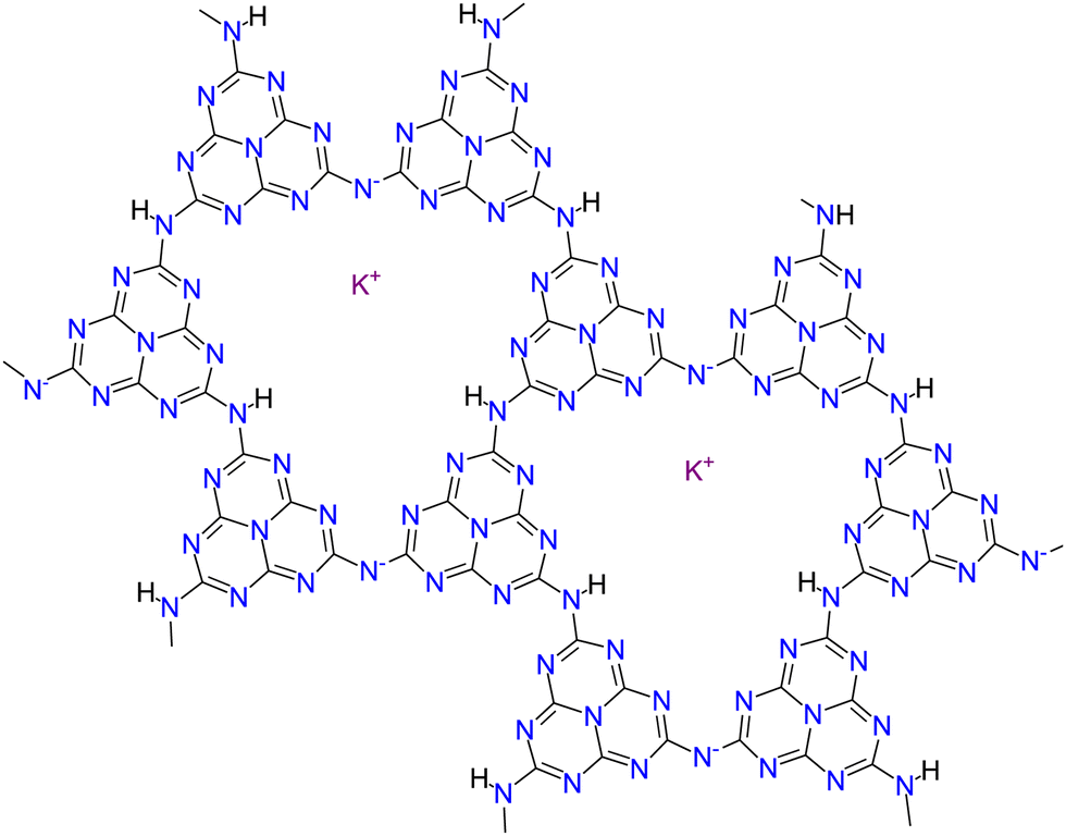 | ||
| Fig. 1 Molecular structure of K-PHI. | ||
Experimental and theoretical
Materials
A single crystal of melem hydrate was obtained after melamine calcination (5 g, purity: 99.0%, Wako Pure Chem., Ind., Ltd, 139-00945) in a tube furnace (KTF035N1/Koyo Thermo Systems Co.) by increasing the temperature to 310 °C at 1 °C min−1, followed by holding for 5 hours and then naturally cooling. The resulting product was washed with N,N-dimethylformamide (DMF) and acetone and dried at 150 °C for 24 h. The dried sample was dissolved in dimethylsulfoxide (DMSO) to obtain melem hydrate single crystals via vapor diffusion. Melon was synthesized in the same way as melem in a tube furnace. Melamine (3 g) was placed at the bottom of a quartz test tube and calcined by increasing the temperature to 550 °C at 1 °C min−1 and holding for 5 h, followed by decreasing the temperature at 2 °C min−1. K-PHI was obtained by mixing melon (0.3 g) and potassium thiocyanate (KSCN, 0.15 g, purity: 98.0%, Wako Pure Chem., Ind., Ltd, 164-04555) and calcining them in a tube furnace by increasing the temperature at 30 °C min−1 and holding for 1 h, followed by further increasing the temperature at 30 °C min−1 and holding for 30 min; then, the temperature was decreased at 2 °C min−1.Thin film fabrication
The as-synthesized melem hydrate single crystals were placed in an aluminum crucible and evaporated onto an Au (300 nm)/Si(100) substrate in an ultra-high vacuum (10−6 Pa) to fabricate a 30 nm thin film. K-PHI was dispersed in N-methyl-2-pyrrolidone (NMP) and sonicated for 60 h for chemical cleavage. The resulting dispersion was separated in a centrifuge overnight, and the supernatant liquid was considered as the K-PHI nanosheet dispersion (Fig. S1(b), ESI†). To this, chlorobenzene was mixed at a ratio of 60 vol%, and the nanosheet was precipitated via centrifugation overnight. The resulting concentrated nanosheet liquid was dropped onto the substrate to obtain the K-PHI thin film. Subsequently, UV-O3 cleaning was performed (UV253E; Filgen) for 30 min, and the cleaning chamber was replaced with oxygen before cleaning. 3, 4, 9, 10-Perylenetetracarboxylic diimide (PTCDI, >95% Tokyo Chemical Industry Co., Ltd P0984) film was fabricated by 30 nm deposition in an ultra-high vacuum in the same way as melem film on the Au (300 nm)/Si(100) substrate.Measurement methods
X-ray diffraction (XRD) analysis was performed (Smart lab, Rigaku), with Cu Ka (0.15496 nm) as the X-ray source. Transmission electron microscopy (TEM) was performed using a JEM-2100F (JEOL), with an acceleration voltage of 80 kV and spherical aberration correction Cs = 0.5 mm, using Cu300 mesh (EM Japan Co., Ltd U1015-F10) as the grid. XPS was performed using JPS-9030 (JEOL), with monochromatized Al Ka (hν = 1486.6 eV) as the X-ray source. UPS equipment was created in the laboratory using SES200 (SCIENTA) as the analyzer, and He Iα (hν = 21.22 eV) as the light source. IPES was similarly performed on the same sample on PSP vacuum technology equipment. The band-pass detector comprised a NaCl-coated Canneltron behind a SrF2 window and detected photons at hν = 9.3 eV. Pulse IV measurements were performed using source measurement units (Keysight Technologies, B2912B). Electrical impedance spectroscopy (EIS) was performed using an LCR meter (Keysight Technologies, E4980A). All the measurements were performed using a 4-probe system at room temperature under atmospheric conditions. The pyZwx software was used to obtain the impedance spectrum and fitted under appropriate equivalent circuit assumptions.29 These electrical measurements were performed on an Au (20 nm)/K-PHI/Au/Si device structure where the top Au electrode had a diameter and thickness of 0.1 mm and 20 nm, respectively.Density functional theory calculations
The density of states (DOS) and partial DOS (PDOS) were all obtained via density functional theory (DFT) simulations (Materials Studio) performed using Dmol3 as the module, DNP as the Dmol3 basis function, and SCAN, an m-GGA, as the electron correlation approximation method.30–32 The cutoff radius of the orbitals was set to 10 Å for all calculations, and the number of k-point meshes was set to only Γ points for the ‘Orbital’ calculation and 9 × 9 × 16 or 1296 points for the other cases. The cutoff radius was determined from the change in total energy, ionization energy, and electron affinity with increasing cutoff radius from 2 Å to 13 Å.Results and discussion
Structural and chemical state analysis of K-PHI
In this paper, before discussing the charge accumulation phenomenon of K-PHI, the K-PHI thin films fabrication and their basic properties are discussed in detail. The mechanism of the charge accumulation of K-PHI is then discussed below, based on the results of experiments using K-PHI thin films as samples. K-PHI thin film was first synthesized, followed by its nanosheets. Specifically, the synthesized K-PHI powder was sonicated in NMP for 60 h and centrifuged. The obtained supernatant liquid was dispersed with K-PHI nanosheets.Fig. 2(a)–(c) show the high-resolution transmission electron microscopy (HRTEM image) of the K-PHI nanosheet, magnified image, and FFT image of the HRTEM image. The K-PHI nanosheet has a size of ∼50 nm and with its c axis perpendicular to the grid. Fig. 2(b) shows that white dots are periodically arranged in the image, with their periodicity corresponding to the yellow circled points labeled 100 at 0.89 nm−1 in the FFT image shown in Fig. 2(c). This indicates that the lattice points are arranged three-fold symmetrically in the K-PHI nanosheet with a spacing of 1.1 nm, which is equal to the distances between the channels in the K-PHI structure and the symmetry of their arrangement. Furthermore, the red circles labeled 110 at 1.56 nm−1 show a three-fold symmetry, which are tilted by 30° with respect to the yellow circles. This result is consistent with a lattice constant of 0.64 nm in the PHI layer of K-PHI. Fig. 2(d) and (e) show the simulated TEM and FFT images of K-PHI, respectively. Fig. 2(d) shows a magnified view of the simulated TEM image and the molecular structure of K-PHI. The lattice of white dots corresponds to the arrangement of channels present in the PHI layer of K-PHI. The simulated FFT image (Fig. 2(e)) shows hexagonally aligned points, as in Fig. 2(c), and their distances from the center are also consistent with those in Fig. 2(e). These results indicate that the K-PHI nanosheet retains periodically aligned channels and its structure is equivalent to that of the PHI layer of K-PHI. K-PHI thin films were fabricated herein by depositing K-PHI nanosheets on the Au substrate. The photographs and UV-vis spectra of the fabricated K-PHI thin films are shown in Fig. S3 (ESI†). Fig. 2(f) shows the XRD results of the as-prepared K-PHI thin film. The out-of-plane and in-plane measurements and diffraction pattern of K-PHI are shown from top to bottom in the same figure. The in-plane measurements show peaks at 2θ = 7.98°, 13.8°, 21.2°, and 27.9°. In particular, the d-spaces of the two low-angle peaks are 1.1 and 0.64 nm, which are consistent with the periodicity observed in Fig. 2(b) and (c). The XRD patterns of the K-PHI thin film do not match those of the K-PHI powder sample (Fig. S3(b) and (c), ESI†).17 The XRD profile of the K-PHI thin film is well explained by the crystal structure model with α = β = 90°, γ = 120°, a = b = 12.78 Å and c = 3.20 Å. Compared with the simulated diffraction pattern, the in-plane measurements show (100), (110), (210), and (001) peaks at low 2θ. In particular, the (001) peak appears strongly in the out-of-plane results, indicating in the K-PHI nanosheet being oriented perpendicular to the substrate. Although K-PHI nanosheet fabrication has been studied previously, its isolation and thin film fabrication have not been investigated yet.33,34 Films fabricated from nanosheets of titanium oxides or niobium oxides are oriented perpendicular to the substrate;35,36 however, the fabrication of oriented films from nanosheets of 2D-COF have not been reported yet. Thus, to the best of our knowledge, this study is the first to report such a method.
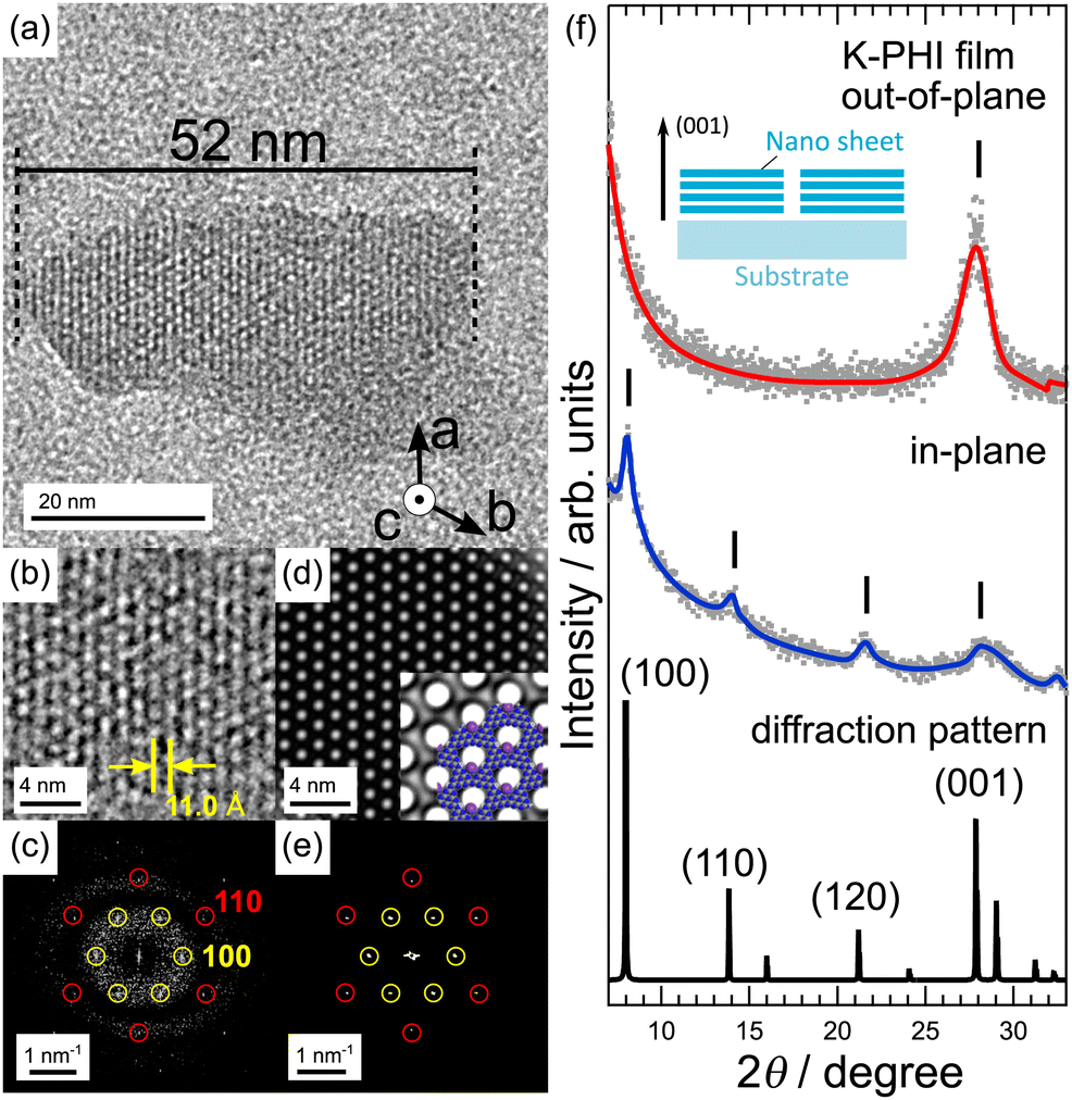 | ||
| Fig. 2 (a) and (b) High-resolution transmission electron microscopy (HRTEM) images of K-PHI nanosheets and its magnified view. (c) Fast Fourier transform (FFT) image of the HRTEM image. Yellow and red circles are located 0.89 and 1.56 nm−1, respectively, from the center. (d) and (e) TEM simulation based on the model structure of K-PHI and its FFT image. The yellow and red circles correspond to those in (c). (f) Thin-film XRD results of K-PHI thin films fabricated by depositing K-PHI nanosheets on the Au substrate. The out-of-plane and in-plane results and the simulated diffraction pattern are shown from top to bottom. The inset shows that the K-PHI nanosheet is oriented perpendicular to the substrate. | ||
The upper panel of Fig. 3(a) shows the N 1s spectrum of the K-PHI thin film and the lower panel shows the N 1s spectrum of the melem film. The fitting analysis results and the observed spectra are also shown; the assignments of the peaks used in the analysis is based on Akaike et al.'s study.37 Specifically, three types of N 1s peaks can be observed: a nitrogen peak with a C–N![[double bond, length as m-dash]](https://www.rsc.org/images/entities/char_e001.gif) C bond (peak Ni), a nitrogen peak linking an amino group or a heptazine ring (peak Nii), and a nitrogen peak attached to three carbons at the center of the heptazine ring (peak Niii). As K-PHI and melem have similar chemical structures, they have similar N peaks. The binding energies of Ni, Nii, and Niii peaks are almost equal, but their intensity ratios are different. The Ni
C bond (peak Ni), a nitrogen peak linking an amino group or a heptazine ring (peak Nii), and a nitrogen peak attached to three carbons at the center of the heptazine ring (peak Niii). As K-PHI and melem have similar chemical structures, they have similar N peaks. The binding energies of Ni, Nii, and Niii peaks are almost equal, but their intensity ratios are different. The Ni![[thin space (1/6-em)]](https://www.rsc.org/images/entities/char_2009.gif) :Nii:Niii ratios for melem and K-PHI were fitted to be 6:3:1 and 12:3:2, respectively, which agree well with the observed data. These ratios are ideal values for each sample, as shown by the molecular structures in Fig. 3(a), indicating that melem and K-PHI thin films have fewer impurities such as intermediate products. A more detailed examination of the binding energies of the peaks shows that the Ni and Niii peaks have shifted by ∼0.1 eV between K-PHI and melem, whereas the Nii peak has shifted by ∼0.4 eV. This chemical shift was caused by a change in the chemical state of Nii from an amino group to an imide bond: the hydrogen bonded to the nitrogen was replaced by carbon with higher electronegativity and the nitrogen was slightly positively charged, resulting in a chemical shift to the higher binding energy side. The Nii peak intensity of K-PHI was smaller than that of melem because during K-PHI synthesis, the amino groups in melem underwent a polymerization reaction that caused the desorption of ammonia and a decrease in the number of Nii peaks. In other words, these changes in the Nii peak indicate that K-PHI was produced via the polymerization of melem. Fig. 3(b) and (c) show the O/N and C/N values obtained from the analysis of the N 1s, C 1s, and O 1s XPS spectra. The average matrix relative sensitivity coefficients were used for elemental sensitivity correction based on the international standards.38 The PTCDI-deposited film, which contained carbon, nitrogen, and oxygen, was used as the reference sample. The error bars are expanded uncertainties based on standard uncertainties obtained from the measurements of the five K-PHI thin films, with k = 2 as the inclusion factor and a confidence level of ∼95%. Quantitative analysis and the related method are described in Note 2 in the ESI.† As shown in Fig. 3(b), the C/N ratio of K-PHI is larger than that of melem because the amount of nitrogen in the sample decreases as the amino group is desorbed from melem during polymerization from melem to K-PHI. The C/N values of K-PHI are consistent with the ideal values of K-PHI within the experimental error. The XPS intensity ratios within the same and between different elements show that the K-PHI thin film is indeed a polymer with a heptazine ring as the building unit and a theoretically predicted K-PHI structure. Lotsch et al. used nuclear magnetic resonance (NMR) to identify the chemical structure of K-PHI and this work firstly reports the identification of chemical structure of K-PHI by quantitative analysis of XPS results.17 As shown in Fig. 3(c), K-PHI has higher O/N values than melem. The oxygen detected in melem is possibly derived from water adhering to the sample surface; thus, K-PHI can be assumed to contain water molecules in its channels that are unique to the crystal structure with the heptazine-based framework. In other words, the large O/N ratio of K-PHI is presumed to be due to the water-derived oxygen in the channels of K-PHI. This is because of the humidity dependence of the ionic conductivity and the requirement of water molecules in the channel for a reasonable interpretation of the XRD results of K-PHI.17,39 These water molecules were not directly observed in the K-PHI. The C/N and O/N results are summarized in Fig. 3(d). The number of carbon and oxygen atoms were counted with respect to the number of nitrogen atoms, which was calculated by multiplying the C/N and O/N values by the number of nitrogen atoms. The K-PHI structure based on the calculated number of atoms contained in the K-PHI structure is shown on the left side of Fig. 3(d) using a space-filling model with van der Waals (vdW) radii. Note that the channel contains approximately five water molecules. The structure of K-PHI in the left figure shows that the channel is almost entirely occupied by these five water molecules and potassium ions. Therefore, the average number of potassium ions in the channel of K-PHI is estimated to be at most one. Thus, the proposed structural model from our previous research may have to be corrected.28,40 Our previous report used a model where the average number of potassium ions in the channel was three, which is inconsistent with the results in Fig. 3 of this paper. However, DFT simulations show that the energy gap was also reduced when one potassium ion bound to the heptazine-based framework in the K-PHI channel was desorbed due to light irradiation (Fig. S7(c), ESI†). This indicates that K-PHI exhibits photochromism associated with potassium ion desorption even if each channel contains only one potassium ion on average.
:Nii:Niii ratios for melem and K-PHI were fitted to be 6:3:1 and 12:3:2, respectively, which agree well with the observed data. These ratios are ideal values for each sample, as shown by the molecular structures in Fig. 3(a), indicating that melem and K-PHI thin films have fewer impurities such as intermediate products. A more detailed examination of the binding energies of the peaks shows that the Ni and Niii peaks have shifted by ∼0.1 eV between K-PHI and melem, whereas the Nii peak has shifted by ∼0.4 eV. This chemical shift was caused by a change in the chemical state of Nii from an amino group to an imide bond: the hydrogen bonded to the nitrogen was replaced by carbon with higher electronegativity and the nitrogen was slightly positively charged, resulting in a chemical shift to the higher binding energy side. The Nii peak intensity of K-PHI was smaller than that of melem because during K-PHI synthesis, the amino groups in melem underwent a polymerization reaction that caused the desorption of ammonia and a decrease in the number of Nii peaks. In other words, these changes in the Nii peak indicate that K-PHI was produced via the polymerization of melem. Fig. 3(b) and (c) show the O/N and C/N values obtained from the analysis of the N 1s, C 1s, and O 1s XPS spectra. The average matrix relative sensitivity coefficients were used for elemental sensitivity correction based on the international standards.38 The PTCDI-deposited film, which contained carbon, nitrogen, and oxygen, was used as the reference sample. The error bars are expanded uncertainties based on standard uncertainties obtained from the measurements of the five K-PHI thin films, with k = 2 as the inclusion factor and a confidence level of ∼95%. Quantitative analysis and the related method are described in Note 2 in the ESI.† As shown in Fig. 3(b), the C/N ratio of K-PHI is larger than that of melem because the amount of nitrogen in the sample decreases as the amino group is desorbed from melem during polymerization from melem to K-PHI. The C/N values of K-PHI are consistent with the ideal values of K-PHI within the experimental error. The XPS intensity ratios within the same and between different elements show that the K-PHI thin film is indeed a polymer with a heptazine ring as the building unit and a theoretically predicted K-PHI structure. Lotsch et al. used nuclear magnetic resonance (NMR) to identify the chemical structure of K-PHI and this work firstly reports the identification of chemical structure of K-PHI by quantitative analysis of XPS results.17 As shown in Fig. 3(c), K-PHI has higher O/N values than melem. The oxygen detected in melem is possibly derived from water adhering to the sample surface; thus, K-PHI can be assumed to contain water molecules in its channels that are unique to the crystal structure with the heptazine-based framework. In other words, the large O/N ratio of K-PHI is presumed to be due to the water-derived oxygen in the channels of K-PHI. This is because of the humidity dependence of the ionic conductivity and the requirement of water molecules in the channel for a reasonable interpretation of the XRD results of K-PHI.17,39 These water molecules were not directly observed in the K-PHI. The C/N and O/N results are summarized in Fig. 3(d). The number of carbon and oxygen atoms were counted with respect to the number of nitrogen atoms, which was calculated by multiplying the C/N and O/N values by the number of nitrogen atoms. The K-PHI structure based on the calculated number of atoms contained in the K-PHI structure is shown on the left side of Fig. 3(d) using a space-filling model with van der Waals (vdW) radii. Note that the channel contains approximately five water molecules. The structure of K-PHI in the left figure shows that the channel is almost entirely occupied by these five water molecules and potassium ions. Therefore, the average number of potassium ions in the channel of K-PHI is estimated to be at most one. Thus, the proposed structural model from our previous research may have to be corrected.28,40 Our previous report used a model where the average number of potassium ions in the channel was three, which is inconsistent with the results in Fig. 3 of this paper. However, DFT simulations show that the energy gap was also reduced when one potassium ion bound to the heptazine-based framework in the K-PHI channel was desorbed due to light irradiation (Fig. S7(c), ESI†). This indicates that K-PHI exhibits photochromism associated with potassium ion desorption even if each channel contains only one potassium ion on average.
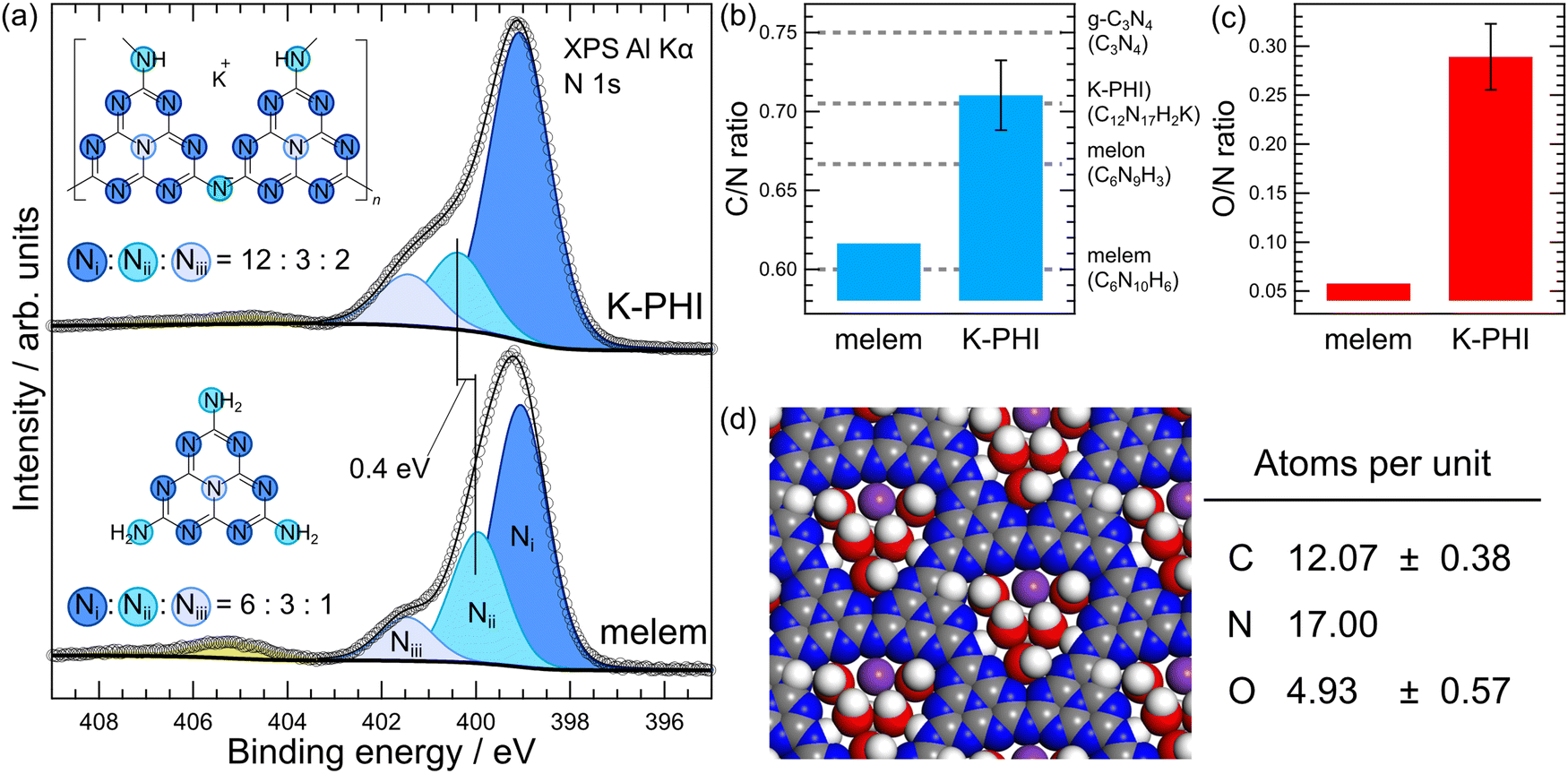 | ||
| Fig. 3 (a) The upper panel shows the XPS N 1s spectrum of the K-PHI thin film, and the lower panel shows the XPS N 1s spectrum of melem. The open circles are measured data, and the solid lines and filled peaks are the results of fitting analysis. The attribution of each peak resolved by fitting analysis is shown in correspondence with the molecular structure, i.e., the color of each peak corresponds to the color of the circle surrounding the nitrogen atom in the molecular structure. The ratio of each peak area obtained from the analysis is also shown. Details of the background subtraction and correction for binding energy are described in Note 2 (ESI†). (b) and (c) Oxygen to nitrogen ratios and carbon to nitrogen ratios of K-PHI and melem obtained from the quantitative analysis of XPS using the AMRSF method. Details of the quantitative analysis of XPS using the AMRSF method are given in Note 2 of the ESI.† Error bars in K-PHI are expanded uncertainties calculated with a coverage factor of k = 2 and have a confidence level of about 95%. (d) Model structure of K-PHI deduced from the analysis results in (b) and (c) by considering the estimated number of atoms of each element per unit cell of K-PHI and the calculated element ratios. All atoms in the molecular structure in (d) are shown according to the space-filling model with van der Waals radius. | ||
To summarize the discussion in this section, the K-PHI nanosheet is a polymer with a heptazine-based framework and each channel of the PHI layer contains, on average, five water molecules and one potassium ion. This result is the first clear indication of the number of water molecules and potassium ions in the K-PHI channels, which remains unclear for powdery K-PHI.
Electronic structure of K-PHI
Fig. 4(a) shows the UPS/IPES spectra of the K-PHI and melem films. The K-PHI thin film was cleaned with UV-O3 for 30 min to remove any surface contamination. The effect of cleaning is discussed in Fig. S2 and S6 (ESI†); however, the K-PHI nanosheet was not damaged during the process. As shown in Fig. 4(a), the blue data denote the observed UPS/IPES spectra, the black solid lines denote the smoothed raw data, and the horizontal axis shows the binding energy measured from the vacuum level. The solid red lines show the spectra with a magnified view near the energy gap, where Ith, Ath and Eg are the ionization energy, electron affinity threshold and energy gap, respectively. Here, Ith and Ath are determined by the cross points between a baseline and a tangent at the inflection points of the first peaks in the UPS and IPES spectra, respectively. Eg can be calculated based on the energy difference between Ith and Ath. The gray hatch-filled spectra denote the DOS obtained from DFT simulations, and the solid and dotted black lines in the hatch represent the N 2p and C 2p PDOS. The structural model determined from the results in Fig. 1 and 2 was used for DFT calculations (Note 3, ESI†). A notable difference in the size of the energy gap is observed in the spectra of K-PHI and melem: the energy gap of K-PHI is ∼1.5 eV smaller than that of melem because of the polymerized structure of K-PHI with melem as the building unit. This observation is consistent with that of Fig. 2. Moreover, the Ith values of K-PHI and melem were not considerably different, but the Ath of K-PHI was considerably smaller than that of melem. To illustrate the changes in ionization energy and electron affinity, Fig. 4(b) shows the energy diagrams for melem, melon, and K-PHI. The left axis represents the binding energy measured from the vacuum level, whereas the numbers in the figure represent Ith and Ath. The Ith and Ath of melon were cited from a previous study.37 The reason for comparing melem, melon and K-PHI here is that these compounds have in common that they are based on the heptazine ring, which makes it easy to compare the differences in electronic structure due to the degree of polymerization. Fig. 4(b) shows that the energy gap decreases in the order of melem, melon, and K-PHI. For melon and K-PHI, the redox levels of water are located within the energy gap. Moreover, melon and K-PHI exhibit photocatalytic activity in visible light, which corresponds with the results reported herein.16,17,41 The Ith and Ath values of melem, melon, and K-PHI are shown in Fig. 4(b). The difference in the Ith and Ath values of these materials are at most ∼0.2 and ∼1.4 eV, respectively. The PDOS in Fig. 4(a) shows that in both K-PHI and melem, a conduction band is formed by almost equal contributions from nitrogen and carbon, whereas a valence band is formed almost exclusively by nitrogen. This suggests that the wave function of the conduction band is delocalized over the molecule or the polymeric framework, whereas that of the valence band is localized to nitrogen. Fig. 4(c) shows the wave functions of the highest occupied molecular orbital (HOMO), HOMO−1, the lowest unoccupied molecular orbital (LUMO), and LUMO+1 of melem and the wave functions of the highest energy band (valence band maximum (VBM)), the second highest energy band (VBM−1) in the valence band, the lowest energy band (conduction band maximum (CBM)), and the second lowest energy band (CBM+1) in the conduction band of K-PHI. The LUMO and LUMO−1 of melem are delocalized over the heptazine ring via a π-bond between nitrogen and carbon. In contrast, the wave functions of HOMO−1 and HOMO are localized to nitrogen, indicating that these orbitals are formed by the lone pairs of nitrogen. These features can also be observed in K-PHI with the same heptazine structure as a building unit. Thus, when melem polymerizes to form K-PHI, the wave function of the valence band of K-PHI remains localized to the lone pair of nitrogen. On the other hand, the LUMO of melem becomes delocalized and a conduction band of K-PHI is formed. Thus, the ionization energy of K-PHI is almost similar to that of melem and only its electron affinity increases. | ||
| Fig. 4 (a) UPS and IPES (UPS/IPES) spectra of K-PHI and melem films. The K-PHI thin film was cleaned with UV-O3. The horizontal axis plots the binding energy measured from the vacuum level. The blue lines show the raw data, the solid black lines show the smoothed spectra of the raw data, and the solid red lines are magnified spectra near the energy gap. Ith, Ath, and Eg represent the ionization energy, electron affinity, and energy gap, respectively. The gray filled spectra show the density of states (DOS) obtained via DFT calculations. The solid black and dotted black lines in the gray region represent the N 2p and C 2p derived partial DOS, respectively. (b) Energy diagrams with Ith and Ath for melem, melon, and K-PHI. The left axis shows the binding energy measured from the vacuum level. The dotted lines indicate the redox levels of water. (c) Wave functions of HOMO−1, HOMO, LUMO, and LUMO+1 for melem and the wave functions of the highest energy band VBM, the second highest energy band VBM−1 in the valence band, the lowest energy band CBM and the second lowest energy band CBM+1 in the conduction band of K-PHI, where the red and green lobes represent the positive and negative signs of the wave functions. VBM and CBM are the valence band maximum and conduction band minimum, respectively. The nitrogen, carbon, hydrogen, and potassium ions are represented by blue, gray, white, and purple spheres, respectively. | ||
The preceding sections cover the fundamental physical properties of K-PHI thin film have been discussed from the viewpoints of crystallography, chemistry, and electronic structure. The subsequent sections will report on the electrical properties of K-PHI thin films.
Electrical properties of K-PHI
Fig. 5(a) shows the results of I–V measurements for the K-PHI thin films. The electric field swept in the order of A, B, C, D, and E. The variation in current in the segment BC is particularly noteworthy. In segment AB, the current increases proportionally to voltage, whereas in segment BC, the current becomes negative as the voltage decreases. This indicates that the current flows in the opposite direction to the applied voltage, which cannot be explained by the carrier conduction of electrons and holes or simple ionic conduction. A similar phenomenon also occurs in segment DEB, indicating that segment BCDE has a characteristic hysteresis curve. These I–V properties can be explained by considering the ionic polarization in K-PHI. As shown in Fig. 2, the K-PHI thin film has a structure of K-PHI nanosheets stacked on the substrate, so the potassium ions can move vertically in the channel with respect to the substrate and electrode surface. Therefore, when the voltage is applied to the top and bottom surfaces of the film, potassium ions move toward the cathode but only slightly shift from the position where they remain charge neutral. The K-PHI thin film shows a large polarization at point B because all the potassium ions in the film move, although the distance traveled by a potassium ion is not large. In segment BC, the polarization built up in the thin film is released as the voltage decreases, thereby generating a current flow in the direction opposite to the applied voltage. In other words, a negative current flow in the external circuit when potassium ions, which have been shifted from their charge-neutral position by the applied voltage, are attracted by the PHI anion and return to their original position. These scenarios are shown in detail in Fig. S10 (ESI†). These findings indicate that the current observed in Fig. 5(a) are polarization currents generated due to the ionic polarization of potassium ions. However, the carrier conduction of electrons and holes in K-PHI cannot be selectively observed in normal I–V measurements because of the non-negligible effect of the hysteresis in the polarization currents. To directly observe carrier conduction in K-PHI, ionic conduction must be suppressed. Herein, the pulse I–V measurement method was used to suppress the hysteresis caused by the polarization current during I–V measurements. The corresponding results are shown in Fig. 5(b). The detailed pulse I–V measurement conditions, such as the interval between pulse voltages, are shown in Fig. S11 (ESI†). Contrary to normal I–V measurements, an interval exists between pulse voltages in pulse I–V measurements during which no voltage is applied. During this interval, the potassium ions in the K-PHI thin film return to their original position before the voltage application, allowing the sample to return from the polarized state to the neutral state. This method of voltage application ensures that it is always applied to the neutral state of the K-PHI during pulse I–V measurements, such that hysteresis associated with ion polarization does not occur. Fig. 5(b) shows that the current flowing in the forward and backward directions of the voltage sweep are almost identical, without significant hysteresis. In the pulse I–V curve, the slope changes around the threshold voltage (Vth).| I = aVm | (1) |
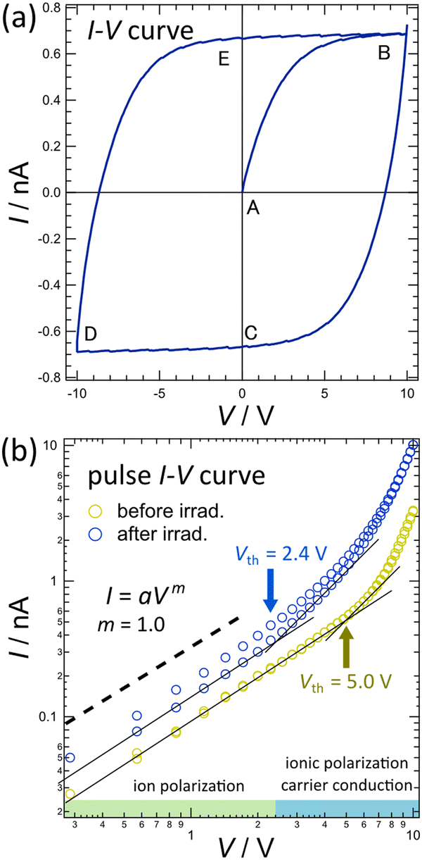 | ||
| Fig. 5 (a) Results of I–V measurements of the K-PHI thin film. I is plotted against V. The electric field is swept in the order A, B, C, D, and E. (b) The double logarithmic graph of pulse I–V measurement results for the K-PHI thin film. The yellow and blue circles show the pulse I–V curve before and after light irradiation, respectively. | ||
Eqn (1) is a general form that represents the voltage dependence of current, where I is the current, V is the voltage, and a is an arbitrary constant. Therefore, Ohmic polarization occurs in the voltage region lower than Vth for the current with m = 1 in eqn (1). Contrarily, carrier conduction occurs in the voltage region higher than Vth, which is expressed as m > 1. When the carrier injection from the electrode is not rate-limiting, carrier conduction in organic semiconductor can be described generally with m ≃ 2 according to the child rule. However, in the voltage region where trap filling is rate-limiting (trap-filling limited), m > 2.42,43 In perovskite materials, where both ionic and carrier conduction is observed, as in K-PHI, m varies based on the balance between ionic and trap densities in the sample.44,45 Carrier conduction occurs in the K-PHI thin film in the high voltage region where m > 1. Moreover, K-PHI exhibits ionic conduction, but we found that carriers can be injected into K-PHI and that it exhibits carrier and ionic conduction.39 The pulse I–V measurement results for the K-PHI thin film in Fig. 5(b) show a change in the current flow due to light irradiation. Two changes were observed in the pulse I–V curves before and after light irradiation. (1) In the low-voltage region, the intercept of the pulse I–V curve after light irradiation increases. The intercept of the I–V curve in double logarithmic graphs in Fig. 5(b) corresponds to a. This indicates that the ionic conductivity of the K-PHI thin film increases with light irradiation. This result is consistent with the desorption of potassium ions in K-PHI due to light irradiation reported previously.28,46 Here, it is beyond the scope of this study to discuss the pH values inside the channel of K-PHI, but H3O+ resulting from the dissociation of water molecules and partially present H+ in the channel would be expected to show high conductivity. The effect of variations in local pH values in the channel on ionic conduction of K-PHI will need to be investigated experimentally in the future, but it is not reasonable to assume here that these conductivities will increase upon light irradiation. (2) Vth before light irradiation is 5.0 V, whereas that after light irradiation considerably reduces to 2.4 V. This decrease in Vth indicates that light irradiation has reduced the carrier injection barrier from the Au electrode to the K-PHI thin film. In general, the carrier injection barrier is determined by the energy difference between the Fermi energy of the electrode metal and the ionization energy or electron affinity of the sample. As shown in Fig. S12 (ESI†), the energy gap of K-PHI is narrowed by photochromism. Thus, a smaller difference in the Fermi energies of the top of the valence band and the bottom of the conduction band and Au electrode is observed. Consequently, Vth is shifted to lower voltages due to a smaller carrier injection barrier caused by the narrowing of the energy gap by light irradiation. Thus, photochromism occurs in K-PHI thin films due to the stimulation by light irradiation, which increases ionic conductivity and decreases the carrier injection barrier. These changes caused by light irradiation considerably alter the optical and electrical properties of K-PHI thin films.
The increase in ionic conductivity upon light irradiation in the K-PHI thin film was further investigated by performing electrical impedance spectroscopy (EIS). Fig. 6(a) shows the response of the impedance magnitude (|Z|) and phase difference (θ) to light irradiation. Here, |Z| is the magnitude of the impedance in the complex plane, and θ is the angle with respect to the real axis of the complex plane. The yellow hatched area indicates the area where the sample was irradiated with light. As shown in Fig. 6(a), the phase difference is 90° before light irradiation; therefore, the impedance has almost only an imaginary component and the K-PHI responds similar to a capacitor. After light irradiation, the phase difference is 15° and the imaginary component in the impedance is considerably reduced to almost a real component, making the K-PHI respond in a similar way to a resistor. Typically, in the absence of an externally applied voltage, many materials respond in a similar way to a capacitor because of the absence of charge carriers within them that can respond to an applied AC voltage. However, if carriers are present in materials that can respond to external fields, such as mobile ions, they respond in a similar way to a resistor. K-PHI responds in a similar way to a capacitor before light irradiation, as is the case with many materials; however, it responds as a resistor upon light irradiation because the potassium ions detach from the heptazine-based framework and become mobile. Fig. 6(b) shows the EIS results at different light intensities. The EIS measurements were performed at equilibrium with saturated impedance at 1000 Hz (Fig. S13 (ESI†)). Without light irradiation, the EIS shows a typical response of a capacitor. In contrast, the EIS spectra obtained at light intensities of 0.24 W m−2 and above show a semicircle that can be fitted by a Randles-type equivalent circuit, with the diameter of the semicircle decreasing with increasing light intensity. For the Randles-type equivalent circuit, the diameter of the semicircle represents the resistance (Rp) of the sample. Fig. 6(b) shows that the resistance of the K-PHI thin film decreases with increasing light intensity: the ionic conductivity of the K-PHI thin film increases with the light intensity. The conductivity is plotted against light intensity in Fig. 6(c), which was calculated from Rp obtained from the results of the fitting analysis of each EIS spectrum. The results show that the ionic conductivity increases linearly with light intensity. It has been reported that the ionic conductivity of K-PHI can be controlled by humidity, and the results here show that the ionic conductivity of K-PHI can also be controlled by the light intensity.39
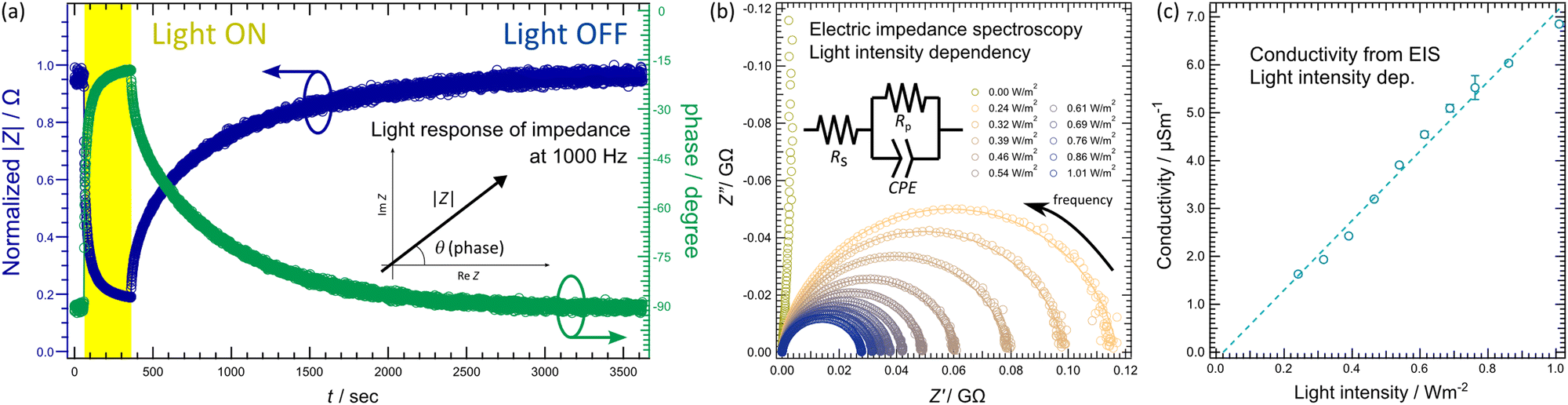 | ||
| Fig. 6 (a) Response of impedance magnitude (|Z|) and phase difference (θ) at 1000 Hz to light irradiation. The yellow hatched areas indicate time frames during which light was irradiated and not irradiated. |Z| and θ in the complex plane are shown in the figure. (b) Electrical impedance spectrum at each light intensity. The circuit in the diagram is the equivalent circuit used for fitting. (c) Light intensity dependence of conductivity obtained from the fitting analysis of the data in (b). The blue dotted line shows the result of linear fitting. | ||
Fig. 6(a) shows the variation in |Z| upon light irradiation, wherein the time constant (τ) of the impedance change is considerably different during and after light irradiation. During light irradiation, τ = 66 s, whereas after light irradiation, τ = 826 s, i.e., approximately 12 times longer. The change in |Z| is caused by the desorption and recombination of potassium ions. However, it is difficult to regard this asymmetry in τ as being caused solely by the thermal motion of the ions. To clarify this finding, other factors that inhibit the recombination of potassium ions with the heptazine-based framework are considered. The desorption of potassium ions from the heptazine-based framework is caused by the transition of K-PHI to an excited state upon light irradiation. Conversely, as long as K-PHI is in an excited state, potassium ions will not recombine into the heptazine-based framework. On the other hand, as mentioned in the introduction, K-PHI is a material that exhibits charge accumulation upon light irradiation. Since the charge accumulation phenomenon is caused by maintaining the excited state generated by light absorption for a long time, the recombination between potassium ions and the heptazine-based framework does not proceed quickly in K-PHI after light irradiation and the impedance gradually changes.
Mechanism of charge accumulation in K-PHI
In this section, we proposed the model to explain the charge-accumulated state (CA) of K-PHI. The ionic conductivity in K-PHI increases upon light irradiation due to photochromism and potassium ion desorption. In addition, CA appears as a stable intermediate state. These phenomena in K-PHI are closely related to each other, which have been explained by developing a model that can comprehensively explain each of these phenomena. Fig. 7(a) shows an energy diagram. The horizontal axis represents the bonding distance between the nitrogen and potassium ions in K-PHI. The experimental fact we obtained in this study is attempted to be explained using this energy diagram. Based on this diagram, we discuss (A) the increase in ionic conductivity and (B) photochromism of K-PHI upon light irradiation. As shown in Fig. 4(c), the wave function of the VBM of K-PHI is localized in the nitrogen bound to the potassium ion, whereas the wavefunction of the excited state of the CBM is spread over the entire heptazine ring. When the electrons of nitrogen in the bridge site, which attracted potassium ions, are excited from the VBM to the CBM, the electron density distribution changes considerably and become delocalized over the heptazine-based framework. Thus, the bond between the potassium ion and nitrogen is cleaved and the potassium ion is desorbed from the heptazine-based framework, causing the system to transition from Y* to B*, followed by the deactivation of B* to B. Here, B* and B are the blue states resulting from the narrowing of the energy gap of K-PHI due to potassium ion desorption, indicative of photochromism. In many photochromic materials, these changes in molecular structure caused by electron density redistribution are responsible for photochromism.47,48 In B, where the N–K bond is cleaved, the energy gap is narrowed and potassium ions released from the heptazine-based framework become more mobile (Fig. S7(c) (ESI†)). These findings explain the phenomena (A) and (B) well. The light intensity dependence of (C) impedance and (D) asymmetry of τ in the dark and light states of the K-PHI is subsequently discussed. Photochromism and ionic conductivity in K-PHI are correlated and photochromism shows a light intensity dependence, as observed in T-type photochromic materials.49–51 This phenomenon generally occurs because the transition to the colored state by light irradiation and the transition to the colorless state by thermal deactivation reach an equilibrium. This equilibrium position is determined by the balance between the excitation rate due to light irradiation and thermal deactivation rate, i.e., the equilibrium position is determined by the light intensity under a constant temperature. A similar equilibrium state also exists between states Y and B in K-PHI, suggesting that the impedance of K-PHI shows light intensity dependence under a constant temperature. The higher the light intensity, the smaller the impedance, and the decrease in impedance saturates with the irradiation time and reaches an equilibrium (Fig. S13(a) (ESI†)). | ||
| Fig. 7 (a) Energy diagram showing the energies of the light-irradiated excited state and the subsequent charge accumulated state of K-PHI. The horizontal axis represents the bonding distance between nitrogen and potassium ions in K-PHI. Y, Y*, B, and B* in the diagram show the color of the sample due to photochromism, representing the ground state (yellow state), the excited state immediately after light absorption (yellow state), the ground state of the K+-desorbed structure (blue state), and the excited state of the K+-desorbed structure (blue state) respectively. CA represents the state in which charges are accumulated on the K-PHI. k1, k2, k3, and k4 represent the rate constants for each reaction, and ΔE represents the activation energy required to relax from CA to B. (b) The molecular structure of K-PHI in yellow and blue states. The blue color in the molecular structure conceptually depicts the electron density in the ground (Y) and excited (B*) states. (c) The left diagram is a schematic of K-PHI in CA. The energy diagram of K-PHI in CA is shown on the right. | ||
We discuss how K-PHI reaches a stable intermediate state CA upon light irradiation. The transition from B to the ground state Y occurs with thermal deactivation at about room temperature. This transition cannot explain the phenomenon shown in Fig. 6(a), where the blue state is maintained for a long time without K+ returning to the heptazine-based framework. Furthermore, after deexcitation from B*, the system presumably transfers directly to the B and then deactivates to Y; only the rate constant k2 is involved in the relaxation. This indicates that the relaxation process of the impedance in K-PHI in the dark state can be described by a simple single exponential function with respect to time. However, as shown in Fig. S13(b) (ESI†), the relaxation process of K-PHI impedance can only be reproduced by the superposition of two exponential functions, indicating that the excited state of K-PHI undergoes two relaxation processes. In addition, the dependence of time constant of the impedance relaxation on light intensity and irradiation time cannot be explained by considering k2 alone (Fig. S14 (ESI†)). This is because the transition from B to Y is caused by thermal deactivation and the rate must be independent of light intensity. These findings indicate that K-PHI does not directly transition from B* to B during the relaxation process in the dark state but via another state. Therefore, a scenario is proposed in which the relaxation from the excited state B* of K-PHI involves a stable intermediate state CA (Fig. 7(c)). CA is a state where photocarriers are accumulated in the blue K-PHI due to the charge separation of excitons in B*. The stabilization of the system with similar charge transfer has also been reported for charge-transfer photochromic materials.48,52 K-PHI deexcited by charge separation from B* has a blue state with a smaller energy gap than the yellow state. Therefore, the blue region of K-PHI works as a shallow trap for electrons and holes as long as it is surrounded by a yellow region with a larger energy gap (left side of Fig. 7(c)). An energy diagram representing this scenario is shown on the right side of Fig. 7(c). To avoid the recombination of charge generated by charge separation and form excitons, the electrons and holes are spatially separated and accumulated in separate blue K-PHI regions (Fig. 7(c)). The charge separation can assume to be facilitated by the electric field gradient created at the boundary between the blue and yellow regions. The accumulated charge is then consumed in the dark state, resulting in the dark photocatalytic activity of K-PHI. Although models of charge accumulation in traps have been developed for other dark photocatalysts, K-PHI is unique as charge is accumulated in a shallow trap formed by its own photochromism.9,13,14,53 We refer to this model as the STCA model.27 Finally, the CA relaxes to B by consuming charge carriers and exciton regeneration and recombination. The charge accumulated in the blue K-PHI region must overcome the energy barrier ΔE corresponding to the energy difference between B and Y to be released from the trap. This is governed by the rate constant k4, which explains another relaxation mechanism observed in the impedance relaxation process upon light irradiation: K-PHI stabilizes in CA during deexcitation, resulting in a large impedance relaxation time constant in the dark state, as shown in the abovementioned experimental fact (D). (D) and the fact that K-PHI exhibits dark photocatalysis suggests that the transition from CA to B takes a long time and k4 is very small. After the accumulated charges are released, excitons regenerate and immediately recombine. Accordingly, K-PHI falls into B, but K+ is reaccommodated in the heptazine-based framework and returns to the ground state Y as the electron density distribution of PHI returns to the same as the ground state Y. Considering its use in dark photocatalysis, if only the holes accumulated in K-PHI are consumed using a hole scavenger such as 4-methyl-benzyl-alcohol (4-MBA), the recombination probability between electrons and holes is even smaller and the state CA is maintained for a longer time.16–18
Conclusions
In this study, K-PHI nanosheets were successfully isolated from K-PHI powder, and K-PHI thin films were subsequently prepared from these nanosheets. XRD and XPS results showed that the chemical and crystal structures of K-PHI thin film and K-PHI were similar. In addition, UPS/IPES measurements were performed to obtain an electronic structure that closely agreed with DFT simulations, and the energy gap, ionization energy, and electron affinity were precisely measured as the fundamental properties of K-PHI. Its electrical properties were also determined. Pulse I–V measurements indicated that K-PHI was an ionic and a carrier conductor and the threshold voltage for carrier conduction shifted due to photochromism. EIS measurements revealed that the ionic conductivity of K-PHI increased proportionally to light intensity and an asymmetry existed in the impedance relaxation process with and without light irradiation, suggesting that K-PHI formed a charge-accumulated state in the dark state. To summarize these results, three phenomena induced by light irradiation in K-PHI, i.e., photochromism, potassium ion desorption, and charge accumulation, were observed with shifts in threshold voltage in the carrier conduction region, a proportional increase in ionic conductivity with light intensity, and long-lived excited states with moderated relaxation. Finally, a model was developed to comprehensively explain these phenomena. The energy diagram suggests the bond between the nitrogen and potassium ions is cleaved during the transition from Y* to B* and the existence of a CA between B* and B of K-PHI. The CA is constituted by charges that accumulate in shallow traps created by photochromism in K-PHI. The discussion of CA is an important insight for understanding and developing dark photocatalyst activity in K-PHI. Moreover, the charge accumulation phenomenon in K-PHI is unique as it does not require bonding with heterogeneous materials and does not involve transition metals. The reported findings thus provide a new opening for the future development of energy-storing photocatalysts.Author contributions
This manuscript was written through contributions of all authors.Data availability
All data included in this study are available upon request by contacting the corresponding author.Conflicts of interest
There are no conflicts to declare.Acknowledgements
The authors gratefully acknowledge Prof. Y. Idemoto and T. Ichihashi for the TEM measurements. This work was supported by JST SPRING, Grant Number JPMJSP2151 and JSPS KAKENHI Grant Number 23KJ1967.Notes and references
- L. Wang and H. Xu, Two-dimensional conjugated polymer frameworks for solar fuel generation from water, Prog. Polym. Sci., 2023, 145, 101734 CrossRef CAS.
- J. Xu, F. A. Roghabadi, Y. Luo, V. Ahmadi, Q. Wang and Z. Wang, et al., Recent advances in heterogeneous catalysis of solar-driven carbon dioxide conversion, J. Environ. Sci., 2024, 140, 165–182 CrossRef CAS PubMed.
- J. D. Xiao, R. Li and H. L. Jiang, Metal–Organic Framework-Based Photocatalysis for Solar Fuel Production, Small Methods, 2023, 7(1), 1–36 CrossRef PubMed.
- Q. Xu, Z. Xia, J. Zhang, Z. Wei, Q. Guo and H. Jin, et al., Recent advances in solar-driven CO2 reduction over g-C3N4-based photocatalysts, Carbon Energy, 2023, 5, 2 Search PubMed.
- D. Matuszko, Influence of the extent and genera of cloud cover on solar radiation intensity, Int. J. Climatol., 2012, 32(15), 2403–2414 CrossRef.
- D. Schmidt, M. D. Hager and U. S. Schubert, Photo-Rechargeable Electric Energy Storage Systems, Adv. Energy Mater., 2016, 6(1), 1–11 Search PubMed.
- N. S. Lewis, An integrated, systems approach to the development of solar fuel generators, Electrochem. Soc. Interface, 2013, 22(2), 43–49 CrossRef CAS.
- I. Ganesh, Conversion of carbon dioxide into methanol - A potential liquid fuel: Fundamental challenges and opportunities (a review), Renewable Sustainable Energy Rev., 2014, 31, 221–257 CrossRef CAS.
- J. Y. Y. Loh, N. P. Kherani and G. A. Ozin, Persistent CO2 photocatalysis for solar fuels in the dark, Nat. Sustainability, 2021, 4(6), 466–473 CrossRef.
- M. Sakar, C. C. Nguyen, M. H. Vu and T. O. Do, Materials and Mechanisms of Photo-Assisted Chemical Reactions under Light and Dark Conditions: Can Day–Night Photocatalysis Be Achieved?, ChemSusChem, 2018, 11(5), 809–820 CrossRef CAS PubMed.
- T. Tatsuma, S. Saitoh, Y. Ohko and A. Fujishima, TiO2-WO3 photoelectrochemical anticorrosion system with an energy storage ability, Chem. Mater., 2001, 13(9), 2838–2842 CrossRef CAS.
- P. M. Stanley, F. Sixt and J. Warnan, Decoupled Solar Energy Storage and Dark Photocatalysis in a 3D Metal–Organic Framework, Adv. Mater., 2023, 35, 1 Search PubMed.
- P. Feng, X. Tang, J. Zhang, Y. Mei and H. Li, Persistent photocatalysis effect of black peony-like BiOCl and its potential full-time photocatalytic applications, RSC Adv., 2017, 7(53), 33241–33247 RSC.
- J. Li, Y. Liu, Z. Zhu, G. Zhang, T. Zou and Z. Zou, et al., A full-sunlight-driven photocatalyst with super long-persistent energy storage ability, Sci. Rep., 2013, 3, 2–7 Search PubMed.
- X. Fu, Y. Kong, M. Wang, T. Cai and Q. Zeng, MXene derived Ti3C2/TiO2/Ag persistent photocatalyst with enhanced electron storage capacity for round-the-clock degradation of organic pollutant, J. Colloid Interface Sci., 2024, 656, 233–240 CrossRef CAS PubMed.
- J. Kröger, A. Jiménez-Solano, G. Savasci, P. Rovó, I. Moudrakovski and K. Küster, et al., Interfacial Engineering for Improved Photocatalysis in a Charge Storing 2D Carbon Nitride: Melamine Functionalized Poly(heptazine imide), Adv. Energy Mater., 2021, 11, 6 Search PubMed.
- H. Schlomberg, J. Kröger, G. Savasci, M. W. Terban, S. Bette and I. Moudrakovski, et al., Structural Insights into Poly(Heptazine Imides): A Light-Storing Carbon Nitride Material for Dark Photocatalysis, Chem. Mater., 2019, 31(18), 7478–7486 CrossRef CAS PubMed.
- V. W. Lau, D. Klose, H. Kasap, F. Podjaski, M. C. Pignié and E. Reisner, et al., Dark Photocatalysis: Storage of Solar Energy in Carbon Nitride for Time-Delayed Hydrogen Generation, Angew. Chem., Int. Ed., 2017, 56(2), 510–514 CrossRef CAS PubMed.
- A. Gouder, A. Jiménez-Solano, N. M. Vargas-Barbosa, F. Podjaski and B. V. Lotsch, Photomemristive sensing via charge storage in 2D carbon nitrides, Mater. Horiz., 2022, 9(7), 1866–1877 RSC.
- V. Sridhar, F. Podjaski, J. Kröger, A. Jiménez-Solano, B. W. Park and B. V. Lotsch, et al., Carbon nitride-based light-driven microswimmers with intrinsic photocharging ability, Proc. Natl. Acad. Sci. U. S. A., 2020, 117(40), 24748–24756 CrossRef CAS PubMed.
- Z. Liu, G. Wang, H. S. Chen and P. Yang, An amorphous/crystalline g-C3N4 homojunction for visible light photocatalysis reactions with superior activity, Chem. Commun., 2018, 54(37), 4720–4723 RSC.
- H. Kim, S. Gim, T. H. Jeon, H. Kim and W. Choi, Distorted Carbon Nitride Structure with Substituted Benzene Moieties for Enhanced Visible Light Photocatalytic Activities, ACS Appl. Mater. Interfaces, 2017, 9(46), 40360–40368 CrossRef CAS PubMed.
- I. Papailias, T. Giannakopoulou, N. Todorova, D. Demotikali, T. Vaimakis and C. Trapalis, Effect of processing temperature on structure and photocatalytic properties of g-C3N4, Appl. Surf. Sci., 2015, 358, 278–286 CrossRef CAS.
- Q. Tay, P. Kanhere, C. F. Ng, S. Chen, S. Chakraborty and A. C. H. Huan, et al., Defect Engineered g-C3N4 for Efficient Visible Light Photocatalytic Hydrogen Production, Chem. Mater., 2015, 27(14), 4930–4933 CrossRef CAS.
- P. Niu, M. Qiao, Y. Li, L. Huang and T. Zhai, Distinctive defects engineering in graphitic carbon nitride for greatly extended visible light photocatalytic hydrogen evolution, Nano Energy, 2018, 44, 73–81 CrossRef CAS.
- A. Rogolino, I. F. Silva, N. V. Tarakina, M. A. R. da Silva, G. F. S. R. Rocha and M. Antonietti, et al., Modified Poly(Heptazine Imides): Minimizing H2O2 Decomposition to Maximize Oxygen Reduction, ACS Appl. Mater. Interfaces, 2022, 14(44), 49820–49829 CrossRef CAS PubMed.
- Y. Markushyna, P. Lamagni, C. Teutloff, J. Catalano, N. Lock and G. Zhang, et al., Green radicals of potassium poly(heptazine imide) using light and benzylamine, J. Mater. Chem. A, 2019, 7(43), 24771–24775 RSC.
- G. Seo, Y. Saito, M. Nakamichi, K. Nakano, K. Tajima and K. Kanai, Mechanism of charge accumulation of poly(heptazine imide) gel, Sci. Rep., 2021, 11(1), 1–12 CrossRef PubMed.
- K. Kobayashi and T. S. Suzuki, Free analysis and visualization programs for electrochemical impedance spectroscopy coded in python, Electrochemistry, 2021, 89(2), 218–222 CrossRef CAS.
- J. Sun, A. Ruzsinszky and J. Perdew, Strongly Constrained and Appropriately Normed Semilocal Density Functional, Phys. Rev. Lett., 2015, 115(3), 1–6 CrossRef PubMed.
- B. Delley, From molecules to solids with the DMol3 approach, J. Chem. Phys., 2000, 113(18), 7756–7764 CrossRef CAS.
- B. Delley, An all-electron numerical method for solving the local density functional for polyatomic molecules, J. Chem. Phys., 1990, 92(1), 508–517 CrossRef CAS.
- C. Zhu, X. Luo, C. Liu, Y. Wang, X. Chen and Y. Wang, et al., Defect-rich ultrathin poly-heptazine-imide-framework nanosheets with alkali-ion doping for photocatalytic solar hydrogen and selective benzylamine oxidation, Nano Res., 2022, 15(10), 8760–8770 CrossRef CAS.
- W. Wang, X. Fan, Z. Shu, J. Zhou and D. Meng, Sustainable and mild exfoliation of bulk crystalline carbon nitride into ultrathin nanosheets via ion-exchange in pure-water, Carbon, 2023, 205, 76–85 CrossRef CAS.
- Y. Shi, M. Osada, Y. Ebina and T. Sasaki, Single droplet assembly for two-dimensional nanosheet tiling, ACS Nano, 2020, 14(11), 15216–15226 CrossRef CAS PubMed.
- M. Osada, K. Akatsuka, Y. Ebina, H. Funakubo, K. Ono and K. Takada, et al., Robust high-κ response in molecularly thin perovskite nanosheets, ACS Nano, 2010, 4(9), 5225–5232 CrossRef CAS PubMed.
- K. Akaike, K. Aoyama, S. Dekubo, A. Onishi and K. Kanai, Characterizing Electronic Structure near the Energy Gap of Graphitic Carbon Nitride Based on Rational Interpretation of Chemical Analysis, Chem. Mater., 2018, 30(7), 2341–2352 CrossRef CAS.
- ISO 18118:2015 Surface chemical analysis—Auger electron spectroscopy and X-ray photoelectron spectroscopy—Guide to the use of experimentally determined relative sensitivity factors for the quantitative analysis of homogeneous materials.
- J. Kröger, F. Podjaski, G. Savasci, I. Moudrakovski, A. Jiménez-Solano and M. W. Terban, et al., Conductivity Mechanism in Ionic 2D Carbon Nitrides: From Hydrated Ion Motion to Enhanced Photocatalysis, Adv. Mater., 2022, 34, 7 CrossRef PubMed.
- M. Hattori, M. Nakamichi, A. Yamaguchi, C. Miyazaki, G. Seo and R. Ohnuki, et al., Influence of Ion Exchange on Photoresponsive Properties of Potassium Poly(heptazine imide), Chem. Mater., 2023, 35(3), 1283–1294 CrossRef CAS.
- V. W. H. Lau, I. Moudrakovski, T. Botari, S. Weinberger, M. B. Mesch and V. Duppel, et al., Rational design of carbon nitride photocatalysts by identification of cyanamide defects as catalytically relevant sites, Nat. Commun., 2016, 7 Search PubMed.
- X. Tang, M. Chen, L. Jiang, M. Li, G. Tang and H. Liu, Improvements in Efficiency and Stability of Perovskite Solar Cells Using a Cesium Chloride Additive, ACS Appl. Mater. Interfaces, 2022, 14(23), 26866–26872 CrossRef CAS PubMed.
- Z. Fang, W. Chen, Y. Shi, J. Zhao, S. Chu and J. Zhang, et al., Dual Passivation of Perovskite Defects for Light-Emitting Diodes with External Quantum Efficiency Exceeding 20%, Adv. Funct. Mater., 2020, 30(12), 1–9 CrossRef.
- V. M. Le Corre, E. A. Duijnstee, O. El Tambouli, J. M. Ball, H. J. Snaith and J. Lim, et al., Revealing Charge Carrier Mobility and Defect Densities in Metal Halide Perovskites via Space-Charge-Limited Current Measurements, ACS Energy Lett., 2021, 6(3), 1087–1094 CrossRef CAS PubMed.
- E. A. Duijnstee, J. M. Ball, V. M. Le Corre, L. J. A. Koster, H. J. Snaith and J. Lim, Toward Understanding Space-Charge Limited Current Measurements on Metal Halide Perovskites, ACS Energy Lett., 2020, 5(2), 376–384 CrossRef CAS.
- M. Nakamichi, M. Hattori, G. Seo, R. Ohnuki, S. Yoshioka and K. Kanai, Formable Optoelectronic Functional Composites with Potassium Poly(heptazine imide), ACS Appl. Electron. Mater., 2022, 4(12), 5747–5751 CrossRef CAS.
- A. Khodko, V. Khomenko, Y. Shynkarenko, O. Mamuta, O. Kapitanchuk and D. Sysoiev, et al., Ultrafast ring-closing reaction dynamics of a photochromic furan-based difurylethene, Chem. Phys. Lett., 2017, 669, 156–160 CrossRef CAS.
- Y. Kobayashi and J. Abe, Recent advances in low-power-threshold nonlinear photochromic materials, Chem. Soc. Rev., 2022, 51(7), 2397–2415 RSC.
- K. Mutoh, Y. Nakagawa, A. Sakamoto, Y. Kobayashi and J. Abe, Stepwise two-photon-gated photochemical reaction in photochromic [2.2]paracyclophane-bridged bis(imidazole dimer), J. Am. Chem. Soc., 2015, 137(17), 5674–5677 CrossRef CAS PubMed.
- I. Yonekawa, K. Mutoh and J. Abe, Visible light intensity dependent negative photochromism of a binaphthyl-bridged phenoxyl-imidazolyl radical complex, Chem. Commun., 2019, 55(9), 1221–1224 RSC.
- I. Yonekawa, K. Mutoh, Y. Kobayashi and J. Abe, Intensity-Dependent Photoresponse of Biphotochromic Molecule Composed of a Negative and a Positive Photochromic Unit, J. Am. Chem. Soc., 2018, 140(3), 1091–1097 CrossRef CAS PubMed.
- Y. Kobayashi, T. Katayama, T. Yamane, K. Setoura, S. Ito and H. Miyasaka, et al., Stepwise two-photon-induced fast photoswitching via electron transfer in higher excited states of photochromic imidazole dimer, J. Am. Chem. Soc., 2016, 138(18), 5930–5938 CrossRef CAS PubMed.
- Z. Zou, X. Tang, C. Wu, D. Wang, J. Zhang and Z. Ci, et al., How to tune trap properties of persistent phosphor: Photostimulated persistent luminescence of NaLuGeO4:Bi3+,Cr3+ tailored by trap engineering, Mater. Res. Bull., 2018, 97, 251–259 CrossRef CAS.
Footnote |
| † Electronic supplementary information (ESI) available. See DOI: https://doi.org/10.1039/d4cp02012j |
| This journal is © the Owner Societies 2024 |