Negative capacitance in Au/CuInGaSe2/SiO2/n-Si/Al Schottky barrier diode devices
Received
11th May 2024
, Accepted 21st August 2024
First published on 22nd August 2024
Abstract
This study pioneers the use of CuInGaSe2, a quaternary alloy, in Schottky barrier diodes, beyond its traditional application in solar cells, highlighting its potential in sustainable energy technologies such as supercapacitors. We delve into its unique electrical and dielectric characteristics by introducing CuInGaSe2 into the Schottky barrier diode device, synthesized via an innovative liquid phase epitaxy on silicon substrates. Our investigation into the structural, electrical, and dielectric properties reveals the alloy's exceptional capacitance behavior, which transitions from positive to negative with varying frequency. It takes negative values at a frequency of 12![[thin space (1/6-em)]](https://www.rsc.org/images/entities/char_2009.gif) 900 Hz and a temperature of 300 K. In comparison, at a frequency of 1216 Hz, all curves take negative and positive values, demonstrating significant promise for enhancing the efficiency and sustainability of energy storage solutions. These findings contribute to the advancement of supercapacitor production and underscore the broader applicability of CuInGaSe2 in promoting sustainable energy technologies.
900 Hz and a temperature of 300 K. In comparison, at a frequency of 1216 Hz, all curves take negative and positive values, demonstrating significant promise for enhancing the efficiency and sustainability of energy storage solutions. These findings contribute to the advancement of supercapacitor production and underscore the broader applicability of CuInGaSe2 in promoting sustainable energy technologies.
Introduction
Copper indium gallium selenide (CuInGaSe2 or CIGS) is a versatile quaternary alloy primarily utilized in high-efficiency thin-film solar cells,1,2 achieving efficiencies over 20%, which are incorporated into solar panels, building-integrated photovoltaics (BIPVs), and portable electronics due to its high absorption coefficient and flexibility on various substrates. Its applications extend to architectural integration, enabling seamless solar integration into building facades, windows, and wearable technologies, offering energy solutions for gadgets like solar-powered watches and clothing. Furthermore, CIGS's robustness against radiation and high efficiency-to-weight ratio make it suitable for spacecraft solar panels, and its potential in powering vehicles and consumer electronics signifies its role in reducing fossil fuel reliance.3–6 These varied applications underscore CIGS's potential in advancing green technology across multiple sectors. CIGSe thin film fabrication has been advanced using non-hydrazine-based solution processes, overcoming previous thickness limitations of about 1.2–1.3 microns.7 Researchers have fabricated CIGSe absorbers up to 2 microns thick by altering the ink formulation and using high-temperature processes. This also helped eliminate the fine-grain layers common in thinner films. This improvement aligns the film morphology with those made using more efficient hydrazine-based methods.8 Electrodeposition is a cost-effective alternative to vacuum-based processes. It involves depositing the metallic elements from an aqueous solution onto a conductive substrate, followed by annealing in the presence of selenium to form a CIGS layer. This method allows for low-cost production and is particularly useful in large-area applications. Bhattacharya et al. comprehensively reviewed the electrodeposition process for CIGS.9 Co-evaporation is one of the most common methods for depositing CIGS layers. This process evaporates copper, indium, gallium, and selenium in a vacuum to form a thin film on a substrate. The advantage of this technique is the precise control it offers over the composition and thickness of the film, which is crucial for achieving high-efficiency solar cells. Studies like those by Rockett and Birkmire provide extensive insights into the process and its optimization.10 CIGSe solar cells with a change efficiency of superior 22% have been manufactured through the multi-process co-evaporation procedure. Still, the implementation of wide-area modules in mass production is limited due to the high product charges.11–13 Hybrid techniques combine elements from different deposition methods to leverage the benefits of each. For instance, combining sputtering for the deposition of metal precursors and rapid thermal processing (RTP) for the selenization step can result in improved film quality and reduced production time. The study by Kim et al. explores such hybrid approaches in detail.14
Sputtering is widely used for manufacturing CIGSe devices and large modules due to its reliable characteristics, ensuring a consistent composition over a large area.15,16 Manufacturing based on the mixing of sputtering ceramic targets and annealing must be further investigated; for example, the device performance, especially the open-circuit voltage (VOC), is lower compared to devices made using the co-evaporation technique.17,18 Enhancement of the device efficiency is related to the increase of VOC;19 an increase in the Ga content in CIGSe-based absorbers causes Eg to expand from 1.04 to 1.68 eV, resulting in an increase in VOC and a decrease in short-circuit current density.20 The optimal efficiency of solar cells can theoretically be obtained when the absorber Eg approaches 1.45 eV; temporarily, the consistent ratio of Ga/(In + Ga) (GGI) for CIGSe devices is 0.6–0.7.21,22 Various researchers in the solar cell fabrication field have investigated CuInGaSe2.
However, we will address the structure of Au/CuInGaSe2/SiO2/n-Si/Al as a Schottky barrier diode, giving the possibility to be used in other applications such as supercapacitors. Several deposition methods have been used for CuInGaSe2 alloys, such as molecular beam epitaxy, sputtering deposition, and metal–organic vapor deposition. To our knowledge, liquid phase epitaxy (LPE) deposition is yet to be investigated. We manufactured CuInGaSe2 on a silicon wafer using (LPE); the prepared structure's structural, electrical, and dielectric properties were investigated by scanning electron microscopy, and I–V and C–V measurements. A comprehensive study of the capacitance behavior of the Au/CuInGaSe2/SiO2/n-Si/Al structure is presented here, and its values change from positive to negative with frequency. It takes negative values at 12900 Hz and 300 K; at a frequency of about 1216 Hz, all curves take negative and positive values. However, at low frequencies of 114 Hz and 30 Hz, all curves take only negative values. The capacitance values were extremely high, indicating that the structure is ideal for supercapacitor manufacturing.
Experimental procedure
The quaternary alloy CuInGaSe2 was synthesized using the liquid phase epitaxy (LPE) technique. The substrate chosen for this procedure was an n-type silicon wafer oriented explicitly along the (100) plane. The raw materials, namely copper (Cu), indium (In), gallium (Ga), and selenium (Se), were sourced from Sigma Aldrich, each with a purity level of 95%. These metallic elements were first dissolved in an indium-based solvent for epitaxial growth. This preparation step was crucial to ensure the formation of a supersaturated solution of CuInGaSe2. The chosen temperature to dissolve the metals in the indium solvent was 1173 Kelvin, which facilitated the formation of a homogeneous alloy solution. As the solution cooled, the crystallization of CuInGaSe2 commenced on the surface of the silicon wafer. This crystallization was primarily influenced by the cooling rate of the solution and the specific interactions between the supersaturated solution and the silicon substrate. These interactions are pivotal as they determine the quality and uniformity of the epitaxial layer formed. The detailed mechanics of the LPE process, including the precise parameters and the conditions under which crystallization was optimized, have been discussed extensively in previously published literature. This foundational knowledge aids in understanding the subtleties of the liquid phase epitaxy technique as applied to the fabrication of CuInGaSe2 thin films.23
A layer of silicon dioxide was formed between CuInGaSe2 and silicon wafers to create the CuInGaSe2/SiO2/n-Si structure, and then two electrodes of gold and aluminum were deposited on the upper and lower surfaces of the unit Au/CuInGaSe2/SiO2/n-Si/Al using thermal evaporation. Fig. 1 presents the XRD pattern of the epitaxial-grown CuInGaSe2 film on a SiO2/Si substrate. In addition to the XRD peak corresponding to Si at 2θ = 68.999°, which is assigned to the diffraction plane (400) for the Si substrate JCPDS PDF no. (00-0787), there are two dispersed small peaks centered at 2θ = 17.5° and 27.2° corresponding to CuGa0.5In0.5Se JCPDS PDF no. (40-1488). These results confirmed the formation of the CuInGaSe2 as a single-phase on the SiO2/Si substrate. Gaussian fitting for XRD peaks at 2θ = 17.5° and 27.2° is performed (Fig. 2), and their FWHM values are estimated. By applying Scherrer's equation,24 the crystallite size could be calculated as follows:
| |  | (1) |
where
λ is the wavelength of the radiation,
β is the width at full width at half maximum intensity,
θ is Bragg's angle, and
K is the Scherrer constant. The estimated crystallite size is 23 and 45 nm as deduced by the XRD peaks at 2
θ =17.5° and 27.2°, respectively. Further morphological details are revealed by SEM imaging, as shown in
Fig. 3, which displays the top surfaces of the CuInGaSe
2 films. The SEM micrographs distinctly illustrate the film's grain sizes and structural arrangement. Such imagery is crucial for assessing the uniformity and quality of the film, as grain boundaries and size can significantly influence the electrical and optical properties of the material. The evident variation in grain size, as visually supported by the SEM analysis, corroborates the XRD findings and highlights the heterogeneity in the crystalline formation across the film. This combination of XRD and SEM analyses is vital for a comprehensive understanding of the film's physical characteristics, directly impacting its potential applications in photovoltaic devices and other semiconductor technologies.
 |
| | Fig. 1 XRD pattern of Au/CuInGaSe2/SiO2/n-Si/Al. | |
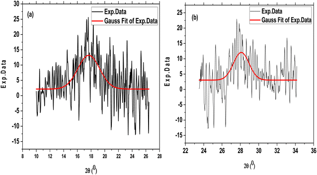 |
| | Fig. 2 Gaussian fit of the XRD peaks at planes (101) (a) and (112) (b) for CuInGaSe2/SiO2/Si. | |
 |
| | Fig. 3 SEM image of Au/CuInGaSe2/SiO2/n-Si/Al. | |
Capacitance properties
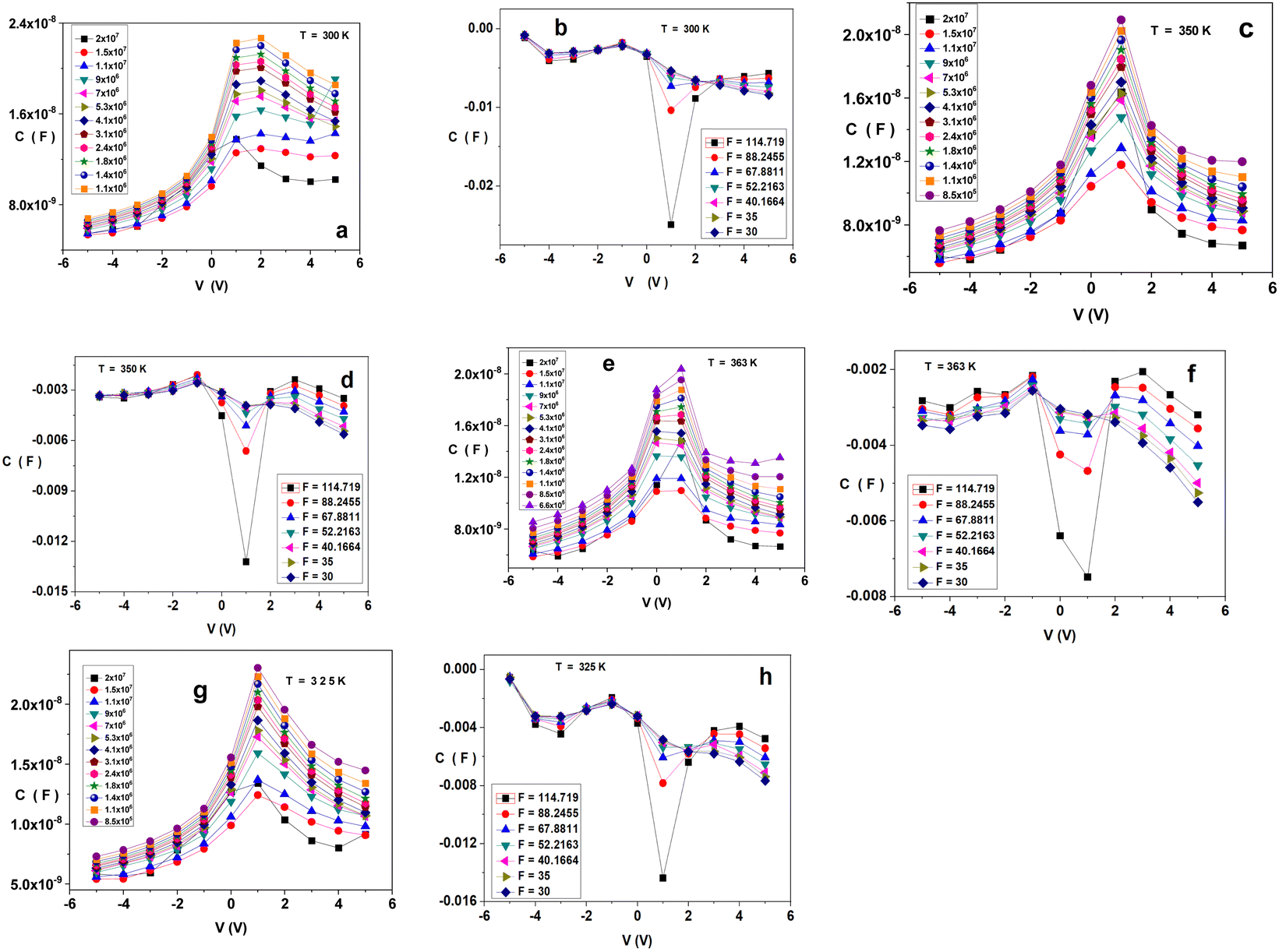
The measurements were performed across a frequency range of 0.1 Hz to 20 MHz and a temperature range of 303 to 423 K using a Novocontrol high-resolution alpha analyzer. The setup included a Quatro temperature controller, which utilized clean nitrogen as a heating agent, ensuring temperature stability within ±0.2 K. This instrument is equipped to provide comprehensive dielectric parameters, including capacitance, conductance, impedance, modulus, dielectric constant, and series resistance, across various frequencies, temperatures, and voltages. The dielectric properties of the Au/CuInGaSe2/SiO2/n-Si/Al structure, as detailed in Fig. 4 (a through g), reveal complex capacitance behaviors dependent on the temperature, voltage, and frequency variations. As the temperature decreases, capacitance notably increases, peaking around 1 V, indicative of thermal sensitivity in the dielectric properties due to potential changes in charge carrier mobility or density. This trend is particularly pronounced at higher frequencies (2 × 10⁷ and 1115970 Hz), where capacitance values remain positive and increase with frequency reduction, suggesting charge dispersion effects related to polarization and charge trapping. The anomalous peak observed in the forward bias region may be attributed to several factors. Firstly, the combined effect of series resistance and charge trapping/de-trapping at the interface states can lead to a noticeable increase in capacitance. Additionally, dielectric relaxation phenomena within the material could contribute to this effect. As the frequency increases, the relaxation processes might not be able to keep up with the applied voltage changes, resulting in a capacitance peak. Furthermore, in forward bias, particularly at higher voltages, there might be an increased injection of minority carriers. This can lead to additional recombination and generation processes, thereby affecting the overall capacitance of the device. At lower frequencies (105236 Hz), increased capacitance in the positive voltage region suggests enhanced charge storage capacity.
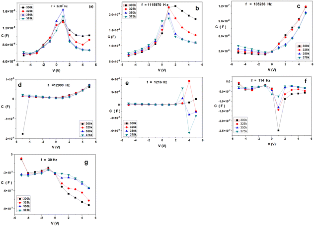 |
| | Fig. 4 (a)–(g) C vs. V at different temperatures and frequencies of Au/CuInGaSe2/SiO2/n-Si/Al. | |
Further reduction in the frequency (12900 and 1216 Hz) results in the capacitance displaying positive and negative values, expanding dramatically in response to voltage changes, which could be linked to complex interfacial charge dynamics involving electrons and holes. Notably, at very low frequencies (114 and 30 Hz), the structure exhibits only negative capacitance values, which might be attributed to border charge loss, series resistance, and ionization processes, possibly exacerbated by interface states (Nss) and series resistance (Rs) as indicated in the literature.25–27 This detailed characterization underscores the intricate interplay between thermal, electrical, and frequency parameters in shaping the dielectric behaviour of this semiconductor structure, highlighting its potential for tailored applications in semiconductor and photovoltaic technologies.
Fig. 5(a) and (b) illustrates the capacitance behavior of the Au/CuInGaSe2/SiO2/n-Si/Al structure as a function of temperature at a constant voltage of V = −5 V across various frequencies. The observed capacitance behavior diverges significantly between low and high-frequency ranges. At low frequencies, the capacitance remains steady at a temperature of 350 K but then decreases, forming peaks at around 360 K, with all recorded values being negative. This suggests a specific thermal response of the dielectric properties at these frequencies, potentially indicative of negative capacitance phenomena related to interfacial charge dynamics or ionization processes that become more pronounced at this temperature range. Conversely, at high frequencies, the capacitance increases as the frequency decreases, remains stable up to 350 K, and then rises to reach maximum values as the temperature grows. The capacitance values in this high-frequency range are consistently positive, highlighting a distinct frequency-dependent thermal sensitivity. These observations, as shown in Fig. 5(a) and (b), suggest complex interactions between temperature, voltage, and frequency that affect the dielectric properties of the structure, which is critical for optimizing device performance in practical applications. The underlying mechanisms likely involve changes in charge carrier dynamics and polarization effects.28–30
 |
| | Fig. 5 (a) and (b) C vs. T at different frequencies and constant Au/CuInGaSe2/SiO2/n-Si/Al voltage. | |
Fig. 6 presents the capacitance variation with frequency at different temperatures and voltages of Au/CuInGaSe2/SiO2/n-Si/Al. The capacitance curves in Fig. 6(a)–(h) all have near-zero values at high and mid frequencies, though the capacitance disperses and takes positive and negative values at low frequencies. The difference is that capacitance curves disperse further at positive V = 5, 4, 3, and 2 V compared to negative voltages. Diodes with imperfections and boundary states can exhibit the NC effect using appropriate bias and frequency;31,32 even the electrons can cross the boundary with enough energy. Electrons collect extra energy and disrupt trapped electrons as they are exposed to a particular bias and frequency. This causes a time delay in the trapped carrier, causing current flow, which corresponds to a non-perfectly phase connection where the current pauses behind the voltage, which causes an inductive effect or negative capacitance effect.33
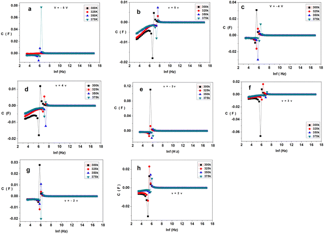 |
| | Fig. 6 (a)–(h) C vs. lnf at different temperatures and voltages of Au/CuInGaSe2/SiO2/n-Si/Al. | |
Fig. 7(a)–(h) shows the capacitance dependence of voltage at different frequencies and temperatures of Au/CuInGaSe2/SiO2/n-Si/Al. The capacitance has the same behavior over various frequencies; it raises with decreasing frequencies and voltage, showing characteristic peaks at about V = 1 V, and it decreases in the positive voltage region. The capacitance at high frequencies has positive values, as displayed in Fig. 7(a), (c), (e) and (g), while at low frequencies, it takes negative values and has the same peak position at about V = 1 V. Negative capacitance means that the materials display inductive performance;34 significantly, the NC phenomenon originates from electron–hole recombination by local traps.35,36 NC dependences on the frequency and bias voltage are reliable with bimolecular recombination, representing that the electron–hole recombination is mediated by trap states and/or materials contamination.32,37
 |
| | Fig. 7 (a)–(h) C vs. V at different frequencies and temperatures of Au/CuInGaSe2/SiO2/n-Si/Al. | |
Fig. 8(a)–(d) showcases the capacitance characteristics of the Au/CuInGaSe2/SiO2/n-Si/Al structure across different frequencies, voltages, and temperatures, revealing critical insights into the device's electrical behavior. Notably, the capacitance exhibits a uniform behavior at high and mid-frequencies, where it is nearly zero, indicating minimal energy storage capability or negligible charge accumulation under these conditions. This consistency suggests a stable dielectric response within these frequency ranges regardless of the applied voltage or ambient temperature.
 |
| | Fig. 8 (a)–(d) C vs. lnf at different voltages and temperatures of Au/CuInGaSe2/SiO2/n-Si/Al. | |
However, at higher frequencies, the scenario shifts dramatically. Here, the capacitance deviates from zero and forms relaxation peaks at each voltage setting. The amplitude of these peaks varies with temperature, and they display both positive and negative values. This behavior indicates complex dielectric relaxation processes occurring within the material, where the dielectric polarization lags the applied electric field at high frequencies. The positive and negative values of the capacitance peaks suggest that the material exhibits both conventional and unconventional (negative) dielectric behaviors depending on the specific voltage and temperature conditions. These phenomena could be attributed to various factors such as interface states, charge trapping, and the movement of charge carriers that respond differently under changing environmental conditions. The detailed analysis provided by Fig. 8(a)–(d) highlights the intricate interplay of frequency, voltage, and temperature in shaping the capacitance behavior of this semiconductor structure, which is essential for understanding its potential applications in electronics and photovoltaics.
I–V current–voltage
The I–V and lnI–V curves of the Au/CuInGaSe2/SiO2/n-Si/Al structure measured at different temperatures are shown in Fig. 9(a) and (b). The thermionic emission (TE) approach describes the process by which electrons overcome the potential energy barrier at the interface of a metal and a semiconductor. According to this theory, the current I flowing through a Schottky diode can be expressed using the following equation:38–40| |  | (2) |
| |  | (3) |
| |  | (4) |
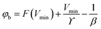
where I0 is the saturation current, Rs is the series resistance, V is the practical voltage, n is the ideality factor, T is the measured temperature in Kelvin, q is the electronic charge, K is the Boltzmann constant, ϕb is the Schottky barrier height (SBH), A* is the Richardson constant, and A is the contact area of the diode.| |  | (5) |
 |
| | Fig. 9 (a) and (b) I, lnI vs. V at different temperatures of Au/CuInGaSe2/SiO2/n-Si/Al. | |
I
0 was distinct by the intersection amid the interpolated straight lines of the lined area and the current axis. The n value can be calculated using eqn (2).41–43 The ϕb, n, and series resistance values of the diode are listed in Table 1.
| |  | (6) |
| |  | (7) |
| |  | (8) |
Table 1 Electrical parameters of a Schottky diode constructed with an Au/CuInGaSe2/SiO2/n-Si/Al structure, evaluated using different theoretical approaches across varying temperatures
|
T (K) |
(I–V) |
Cheung (H) |
dV/dlnI |
Nord (F) |
|
n
|
ϕ
h (eV) |
R
s (Ω) |
n
|
ϕ
h (eV) |
R
s (Ω) |
n
|
R
s (Ω) |
n
|
ϕ
h (eV) |
R
s (Ω) |
| 30 |
10.85 |
0.64 |
6.7 × 10³ |
8.28 |
0.24 |
6.71 × 10³ |
8.28 |
7.12 × 10³ |
10.85 |
0.68 |
7.45 × 10⁴ |
| 50 |
9.89 |
0.76 |
6.2 × 10³ |
6.82 |
0.25 |
7.69 × 10³ |
6.82 |
5.58 × 10³ |
9.89 |
0.71 |
4.20 × 10⁴ |
| 75 |
7.98 |
0.75 |
1.13 × 10⁴ |
5.42 |
0.29 |
1.76 × 10⁴ |
5.42 |
1.34 × 10⁴ |
7.98 |
0.78 |
5.77 × 10⁴ |
| 100 |
6.29 |
0.82 |
1.54 × 10⁴ |
2.62 |
0.30 |
4.71 × 10⁴ |
2.62 |
3.69 × 10⁴ |
6.29 |
0.83 |
3.43 × 10⁴ |
| 125 |
6.03 |
0.85 |
1.20 × 10⁴ |
1.60 |
0.33 |
3.19 × 10⁴ |
1.60 |
2.13 × 10⁴ |
6.03 |
0.87 |
4.20 × 10⁴ |
Fig. 10 shows the analysis of the Au/CuInGaSe2/SiO2/n-Si/Al structure and illustrates the conduction mechanisms via a double-logarithmic (logI vs. logV) presentation under forward bias across a temperature range of 300–400 K. The curves exhibit two distinct linear segments with varying slopes based on the applied voltage. At lower voltages (V ≤ 0.6 V), the I–V relationship is linear with a slope of approximately 1, suggesting ohmic conduction where current increases linearly with voltage. This region reflects the unimpeded flow of charge carriers across a potential gradient. However, as the voltage increases beyond 0.6 V up to 2 V, the slope changes to between 2.2 and 2.9, indicating a transition to space charge limited conduction (SCLC). SCLC suggests that the external voltage drives the current and is also significantly influenced by the internal electric fields due to accumulated charge carriers, which is typical in scenarios with high defect densities or deep traps. This behavior under higher voltage settings highlights robust charge injection and carrier transport capabilities, suggesting that the device can handle high-power applications efficiently, even at elevated temperatures. Understanding these transitions in conduction mechanisms is vital for optimizing the junction's design and enhancing its performance across various operating conditions.44
 |
| | Fig. 10 lnI vs. lnV at different Au/CuInGaSe2/SiO2/n-Si/Al temperatures. | |
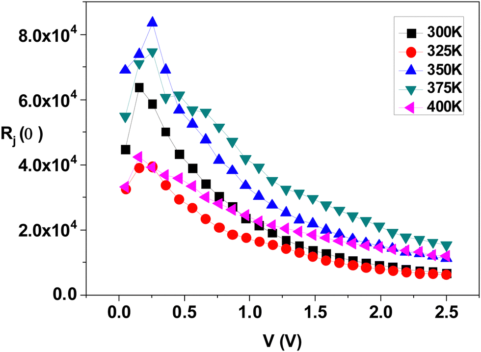
Fig. 11 confirms that the device has a good rectification ratio. Fig. 12 illustrates the variation of junction resistance (Rj) with voltage, allowing the series and shunt resistances to be calculated; as seen in Fig. 13 and 14, both decrease with an increase in temperature.
 |
| | Fig. 11
R
R
vs. V at different Au/CuInGaSe2/SiO2/n-Si/Al temperatures. | |
 |
| | Fig. 12
R
j
vs. V at different Au/CuInGaSe2/SiO2/n-Si/Al temperatures. | |
 |
| | Fig. 13
R
s
vs. T of Au/CuInGaSe2/SiO2/n-Si/Al. | |
 |
| | Fig. 14
R
sh
vs. T of Au/CuInGaSe2/SiO2/n-Si/Al. | |
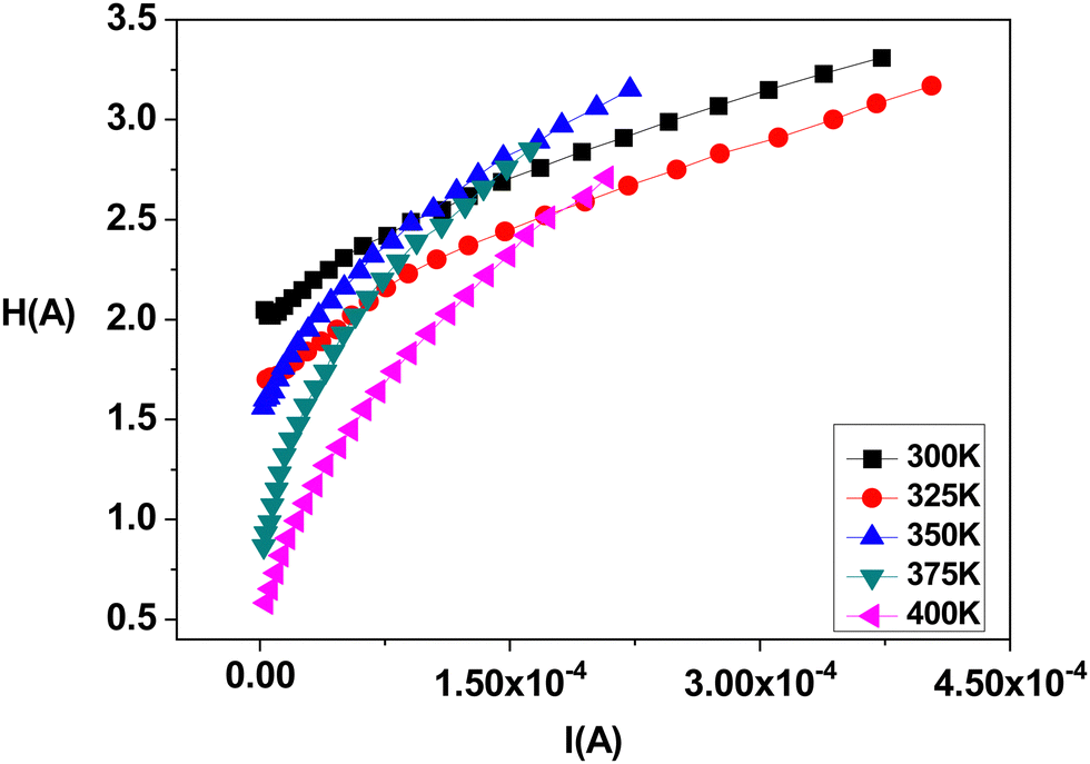
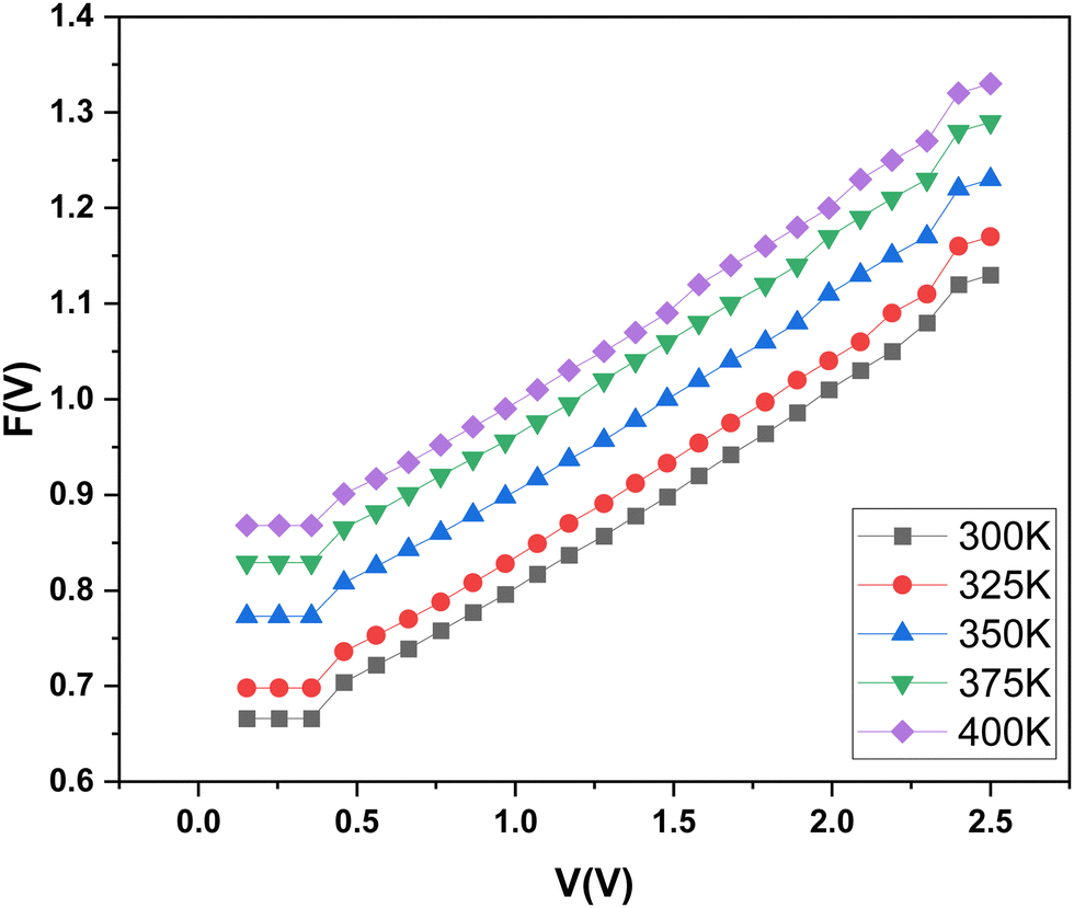
Regarding Cheung's method, Rs and n can be determined by intersecting the slope from the lined area of the dV/d(lnI) and H(I) curves.45–49 As shown in Fig. 15 and 16, calculations shown in eqn (5) and (8) presented the values of Rs and n that are listed in Table 1. The prepared MOS Schottky diode has a high Rs value as there was a thin film of SiO2 layer amid the metal and semiconductor. The Norde equation was also used to determine the ϕb value of the diodes. The Norde function is described as the F(V) vs. the voltage V, as shown in Fig. 17.50,51
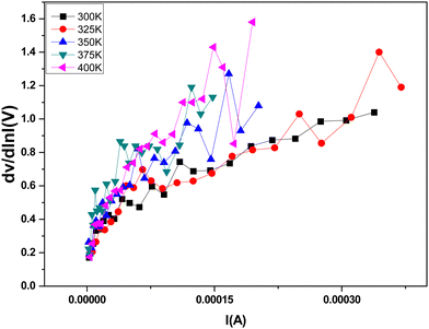 |
| | Fig. 15 dV/dlnI vs. I at different temperatures of Au/CuInGaSe2/SiO2/n-Si/Al. | |
 |
| | Fig. 16
H(I) vs. I at different temperatures of Au/CuInGaSe2/SiO2/n-Si/Al. | |
 |
| | Fig. 17
F(V) vs. V at different temperatures of Au/CuInGaSe2/SiO2/n-Si/Al. | |
Table 1 presents the electrical parameters of a Schottky diode constructed with an Au/CuInGaSe2/SiO2/n-Si/Al structure, evaluated using different theoretical approaches across varying temperatures. The parameters provided include the diode's barrier height (ϕb), ideality factor (n), and series resistance (Rs), which are essential for characterizing the diode's performance and understanding its behavior under different conditions. The data are organized to reflect the outcomes from various theoretical models and temperature settings. Generally, the series resistance decreases as the temperature increases, which suggests improved conductivity. Barrier heights and ideality factors also show variations that indicate different charge carrier dynamics at elevated temperatures. This comprehensive data set is crucial for understanding the impact of temperature on the diode's performance and optimizing its use in various applications.
Conclusions
This study introduced a novel approach to studying the CuInGaSe2 alloy, a material crucial to the modern solar cell industry but explored here for its potential in microelectronic applications, particularly as a Schottky diode and supercapacitor. For the first time, CuInGaSe2 was grown on a silicon wafer using liquid phase epitaxy, highlighting an innovative method of layer deposition that could enhance the performance of semiconductor devices. The study comprehensively examined the structural, electrical, and dielectric properties of the Au/CuInGaSe2/SiO2/n-Si/Al structure through various techniques. Scanning electron microscopy provided insights into the material's morphology, while I–V and C–V measurements assessed its electrical and dielectric behaviors. X-ray diffraction analysis confirmed the successful formation of a single-phase CuInGaSe2 on the SiO2/Si substrate, indicating good crystallinity and structural integrity. Capacitance measurements were particularly revealing, showing negative values at a frequency of 12900 Hz and a temperature of 300 K, which suggests unusual dielectric properties that may be advantageous for specific applications. At around 1216 Hz, the capacitance showed both negative and positive values, and at even lower frequencies of 114 Hz and 30 Hz, it consistently showed negative values. These results indicate a complex interplay of charge dynamics within the material, influenced by frequency and temperature. Most notably, the observed high capacitance levels at these frequencies demonstrate the structure's excellent potential for use in supercapacitors. The ability to handle such high capacitance levels makes this CuInGaSe2-based structure a promising candidate for energy storage applications, where high efficiency and reliability are paramount. Overall, the findings from this work not only enhance our understanding of CuInGaSe2 in microelectronic applications but also open up new avenues for using this versatile material in advanced technological applications.
Data availability
The data supporting this article have been included as part of the article.
Conflicts of interest
The authors declare no conflicts of interest.
References
- R. Sun, D. Zhuang, M. Zhao, Q. Gong, Y. Wei and G. Ren,
et al., Cu2ZnSnSSe4 solar cells with 9.6% efficiency via selenizing Cu-Zn-Sn-S precursor sputtered from a quaternary target, Solar Energy Mater. Solar Cells, 2018, 174, 42–49, DOI:10.1016/j.solmat.2017.08.011.
- Y. Lian, J. Zhang, X. Ma, P. Yang and M. An, Synthesizing three-dimensional ordered macroporous CuInxGa1−xSe2 thin films by template-assisted electrodeposition from modified ionic liquid, Ceram. Int., 2018, 44, 2599–2602, DOI:10.1016/j.ceramint.2017.10.171.
- P. Jackson, D. Hariskos, E. Lotter, S. Paetel, R. Wuerz and R. Menner,
et al., New world record efficiency for Cu(In,Ga)Se2 thin-film solar cells beyond 20%, Prog. Photovoltaics Res. Appl., 2011, 19, 894–897, DOI:10.1002/PIP.1078.
- N. Delen, S. A. Yerişkin, A. Özbay and İ. Taşçıoğlu, Origin of frequency and voltage dependent negative dielectric properties in the Al/p-Si Schottky diodes with (Cd0.3Zn0.7O) interfacial layer in the wide range of frequency and voltage, Phys. B, 2023, 665, 415031, DOI:10.1016/j.physb.2023.415031.
- A. F. Özdemir, Z. Kotan, D. A. Aldemir and S. Altndal, The effects of the temperature on I-V and C-V characteristics of Al/P2ClAn(C2H5COOH)/p-Si/Al structure, EPJ Appl. Phys., 2009, 46, DOI:10.1051/EPJAP/2009035.
- E. Erbilen Tanrıkulu, Variation of electrical and dielectric characteristics of Schottky diodes (SDs) depending on the existence of PVC and carbon-nanotube (CNT)-doped PVC interlayers, J. Mater. Sci.: Mater. Electron., 2023, 34, DOI:10.1007/S10854-022-09479-W.
- S. A. Yerişkin, G. E. Demir and İ. Yücedag, On the Frequency-Voltage Dependence Profile of Complex Dielectric, Complex Electric Modulus and Electrical Conductivity in Al/ZnO/p -GaAs Type Structure at Room Temperature, J. Nanoelectron. Optoelectron., 2019, 14, 1126–1132, DOI:10.1166/JNO.2019.2623.
- S. D. Deshmukh, K. G. Weideman, R. G. Ellis, K. Kisslinger and R. Agrawal, Enabling fine-grain free 2-micron thick CISe/CIGSe film fabrication via a non-hydrazine based solution processing route, Mater. Adv., 2022, 3, 3293–3302, 10.1039/D2MA00095D.
- M. Saeed and O. Israel González Peña, Mass Transfer Study on Improved Chemistry for Electrodeposition of Copper Indium Gallium Selenide (CIGS) Compound for Photovoltaics Applications, Nanomaterials, 2021, 11, 1222, DOI:10.3390/nano11051222.
- Y. C. Lin, S. J. Wei, Y. J. Liang and W. J. Syus, A simple non-toxic simultaneous selenization/sulfurization process for Cu(In, Ga)(S, Se)2 solar cells, Mater. Chem. Phys., 2018, 219, 283–291, DOI:10.1016/J.MATCHEMPHYS.2018.08.045.
- W. Thongkham, A. Pankiew, K. Yoodee and S. Chatraphorn, Enhancing efficiency of Cu(In,Ga)Se2 solar cells on flexible stainless steel foils using NaF co-evaporation, Sol. Energy, 2013, 92, 189–195, DOI:10.1016/j.solener.2013.03.010.
- P. Reinhard, A. Chirilă, P. Blösch, F. Pianezzi, S. Nishiwaki and S. Buecheler,
et al., Review of Progress Toward 20% Efficiency Flexible CIGS Solar Cells and Manufacturing Issues of Solar Modules, IEEE J. Photovolt., 2013, 3, 572–580, DOI:10.1109/JPHOTOV.2012.2226869.
- L. Zhang, D. Zhuang, M. Zhao, Q. Gong, L. Guo and L. Ouyang,
et al., The effects of selenium content on Cu(InGa)Se2 thin film solar cells by sputtering from quaternary target with Se-free post annealing, Vacuum, 2017, 137, 205–208, DOI:10.1016/j.vacuum.2016.12.041.
- M. Acciarri, A. Le Donne, S. Marchionna, M. Meschia, J. Parravicini, A. Gasparotto and S. Binetti, CIGS thin films grown by hybrid sputtering-evaporation method: Properties and PV performance, Solar Energy, 2018, 175, 16–24 CrossRef CAS.
- J. C. Park, M. Al-Jassim, S. W. Shin, J. H. Kim and T. W. Kim, Comprehensive characterization of CIGS absorber layers grown by one-step sputtering process, Ceram. Int., 2019, 45, 4424–4430, DOI:10.1016/j.ceramint.2018.11.120.
- H. X. Zhang and R. J. Hong, CIGS absorbing layers prepared by RF magnetron sputtering from a single quaternary target, Ceram. Int., 2016, 42, 14543–14547, DOI:10.1016/j.ceramint.2016.06.067.
- X. Peng, M. Zhao, D. Zhuang, R. Sun, L. Zhang and Y. Wei,
et al., Study on how the content of selenium in the precursors influences the properties of CuInSe2 thin films, Appl. Surf. Sci., 2018, 434, 452–455, DOI:10.1016/j.apsusc.2017.10.139.
- M. Acciarri, A. Le Donne, S. Marchionna, M. Meschia, J. Parravicini and A. Gasparotto,
et al., CIGS thin films grown by hybrid sputtering-evaporation method: Properties and PV performance, Sol. Energy, 2018, 175, 16–24, DOI:10.1016/j.solener.2018.02.024.
- J. Ramanujam and U. P. Singh, Copper indium gallium selenide based solar cells – a review, Energy Environ. Sci., 2017, 10, 1306–1319, 10.1039/C7EE00826K.
- M. Behr, M. Sharma, S. Sprague, N. Shinkel, J. Kerbleski and C. Alvey,
et al., Effect of growth conditions on microstructure of sputtered precursor for CuIn1-xGaxSe2 (CIGS) absorber layer deposited on stainless steel substrates, Thin Solid Films, 2018, 665, 36–45, DOI:10.1016/j.tsf.2018.08.045.
- M. Saifullah, J. H. Moon, S. Ahn, J. Gwak, S. Ahn and K. Kim,
et al., Effect of Cu content on the photovoltaic properties of wide bandgap CIGS thin-film solar cells prepared by single-stage process, Curr. Appl. Phys., 2016, 16, 1517–1522, DOI:10.1016/j.cap.2016.08.019.
- S. Béchu, A. Loubat, M. Bouttemy, J. Vigneron, J.-L. Gentner and A. Etcheberry, A challenge for x-ray photoelectron spectroscopy characterization of Cu(In,Ga)Se2 absorbers: The accurate quantification of Ga/(Ga + In) ratio, Thin Solid Films, 2019, 669, 425–429, DOI:10.1016/j.tsf.2018.11.029.
- A. Tataroglu, A. Buyukbas Ulusan, Ş. Altındal and Y. Azizian-Kalandaragh, A Compare Study on Electrical Properties of MS Diodes with and Without CoFe2O4-PVP Interlayer, J. Inorg. Organomet. Polym. Mater., 2021, 31, 1668–1675, DOI:10.1007/S10904-020-01798-X/TABLES/2.
-
P. Scherrer in Bestimmung der inneren Struktur und der Größe von Kolloidteilchen mittels Röntgenstrahlen BT, Kolloidchemie Ein Lehrbuch. ed. Zsigmondy R., Springer Berlin Heidelberg, Berlin, Heidelberg, 1912, 387–409. DOI:10.1007/978-3-662-33915-2_7.
- E. Leung, T. Broadhurst, J. Lim, S. A. Rodney, B. Patel and D. Scolnic,
et al., Structural, Optical and Optoelectrical Properties of CuAlSnS4 Thin Films, ECS J. Solid State Sci. Technol., 2024, 13, 035002, DOI:10.1149/2162-8777/AD3366.
- S. Y. Gezgin, Kiliç HŞ. The Effect of Ag and Au Contacts on the Efficiency of CZTS/n-Si Solar Cell: the Confirmation of Experimental and Theoretical Results by SCAPS Simulation, Braz. J. Phys., 2022, 52, 1–10, DOI:10.1007/S13538-022-01145-0/FIGURES/8.
- T. Çakıcı, A. Ajjaq, A. O. Çağırtekin, Ö. Barin, M. Özdal and S. Acar, Surface activation of Si-based Schottky diodes by bacterial biosynthesized AgInSe2 trimetallic alloy nanoparticles with evidenced negative capacitance and enhanced electro-dielectric performance, Appl. Surf. Sci., 2023, 631, 157522, DOI:10.1016/J.APSUSC.2023.157522.
- Ö. Güllü, Dielectric spectroscopy studies on AL/p-Si photovoltaic diodes with Coomassie Brilliant Blue G-250, Appl. Phys. A: Mater. Sci. Process., 2022, 128, 1–14, DOI:10.1007/S00339-022-05729-0/FIGURES/33.
- N. Tuğluoğlu, S. Eymur and N. Turan, Investigation of inhomogeneous device parameters by current–voltage characteristics of identically prepared lateral Schottky diodes with tin oxide interface layer, J. Mater. Sci.: Mater. Electron., 2023, 34, 1–9, DOI:10.1007/S10854-022-09659-8/FIGURES/13.
- M. A. Mohamed, S. E. Zaki, K. Rahmani, R. En-nadir and Y. R. Eker, Negative Photoconductivity in 2D α-MoO3/Ir Self-Powered Photodetector: Impact of Post-Annealing, Materials, 2023, 16, 6756, DOI:10.3390/MA16206756/S1.
- A. Ashery, S. A. Gad, G. M. Turky and A. E. H. Gaballah, Negative Capacitance, Negative Resistance in CNT/TiO2/SiO2/p-Si Heterostructure for Light-Emitting Diode Applications, ECS J. Solid State Sci. Technol., 2021, 10, 31006, DOI:10.1149/2162-8777/abed9a.
- C. Lungenschmied, E. Ehrenfreund and N. S. Sariciftci, Negative capacitance and its photo-inhibition in organic bulk heterojunction devices, Org. Electron., 2009, 10, 115–118, DOI:10.1016/j.orgel.2008.10.011.
- L. E. Byrum, G. Ariyawansa, R. C. Jayasinghe, N. Dietz, A. G. U. Perera and S. G. Matsik,
et al., Negative capacitance in GaN/AlGaN heterojunction dual-band detectors, J. Appl. Phys., 2009, 106, 53701, DOI:10.1063/1.3211292.
- M. Yalcin and F. Yakuphanoglu, Graphene-TiO2 Nanocomposite Photoanode Based on Quantum Dot Solar Cells, J. Nanoelectron. Optoelectron., 2017, 12, 254–259, DOI:10.1166/jno.2017.1952.
- M. Ershov, H. C. Liu, L. Li, M. Buchanan, Z. R. Wasilewski and A. K. Jonscher, Negative capacitance effect in semiconductor devices, IEEE Trans. Electron Devices, 1998, 45, 2196–2206, DOI:10.1109/16.725254.
-
A. A. Al, R. K. Gupta, Y. Al, F. El Tantawy and F. Yakuphanoglu, Efficiency enhancement and transient photocapacitance characteristics of the silicon solar cell by graphene oxide 2015;1:11–14.
- E. Ehrenfreund, C. Lungenschmied, G. Dennler, H. Neugebauer and N. S. Sariciftci, Negative capacitance in organic semiconductor devices: Bipolar injection and charge recombination mechanism, Appl. Phys. Lett., 2007, 91, 12112, DOI:10.1063/1.2752024.
-
B. P. Modi and J. M. Dhimmar The temperature dependent ideality factor effect on I-V characteristics of Schottky diode. Proceedings on 2012 1st International Conference on Emerging Technology Trends in Electronics, Communication and Networking, ET2ECN 2012 2012. 10.1109/ET2ECN.2012.6470063.
- A. Tataroǧlu and Ş. Altindal, The analysis of the series resistance and interface states of MIS Schottky diodes at high temperatures using I–V characteristics, J. Alloys Compd., 2009, 484, 405–409, DOI:10.1016/J.JALLCOM.2009.04.119.
- A. Turut, Analysis of temperature-dependent current–voltage characteristics of Schottky diodes by the modified thermionic emission current model, J. Vacuum Sci. Technol. B, 2024, 42, DOI:10.1116/6.0003463.
- V. Rajagopal Reddy and P. Koteswara Rao, Annealing Temperature Effect on Electrical and Structural Properties of Cu/Au Schottky Contacts to n-Type GaN, Microelectron. Eng., 2008, 85, 470–476 CrossRef.
- T. T. A. Tuan, D.-H. Kuo, C.-C. Li and G.-Z. Li, Effect of Temperature Dependence on Electrical Characterization of p-n GaN Diode Fabricated by RF Magnetron Sputtering, Mater. Sci. Appl., 2015, 06, 809–817, DOI:10.4236/msa.2015.69083.
- B. Barış, Analysis of device parameters for Au/tin oxide/n-Si(100) metal–oxide–semiconductor (MOS) diodes, Phys. Rev. B: Condens. Matter Mater. Phys., 2014, 438, 65–69, DOI:10.1016/j.physb.2014.01.009.
- F. Yakuphanoglu, N. Tugluoglu and S. Karadeniz, Space charge-limited conduction in Ag/p-Si Schottky diode, Phys. Rev. B: Condens. Matter Mater. Phys., 2007, 392, 188–191, DOI:10.1016/j.physb.2006.11.018.
- T. A. Thi, D.-H. Kuo, P. T. Cao, P. Quoc-Phong, V. K. Nghi and N. P. Tran, Electrical and Structural Properties of All-Sputtered Al/SiO2/p-GaN MOS Schottky Diode, Coatings, 2019, 9, DOI:10.3390/coatings9100685.
- C. K. Ramesh, V. R. Reddy and C.-J. Choi, Electrical characteristics of molybdenum Schottky contacts on n-type GaN, Mater. Sci. Eng., B, 2004, 112, 30–33, DOI:10.1016/j.mseb.2004.05.005.
- S. K. Cheung and N. W. Cheung, Extraction of Schottky diode parameters from forward current-voltage characteristics, Appl. Phys. Lett., 1986, 49, 85–87, DOI:10.1063/1.97359.
- T. T. A. Tuan, D.-H. Kuo, A. D. Saragih and G.-Z. Li, Electrical properties of RF-sputtered Zn-doped GaN films and p-Zn-GaN/n-Si hetero junction diode with low leakage current of 10–9A and a high rectification ratio above 105, Mater. Sci. Eng., B, 2017, 222, 18–25, DOI:10.1016/j.mseb.2017.04.008.
- K. Çınar, N. Yıldırım, C. Coşkun and A. Turut, Temperature dependence of current-voltage characteristics in highly doped Ag/p-GaN/In Schottky diodes, J. Appl. Phys., 2009, 106, 73717, DOI:10.1063/1.3236647.
- T. T. A. Tuan, D.-H. Kuo, C.-C. Li and W.-C. Yen, Schottky barrier characteristics of Pt contacts to all sputtering-made n-type GaN and MOS diodes, J. Mater. Sci.: Mater. Electron., 2014, 25, 3264–3270, DOI:10.1007/s10854-014-2012-1.
- H. Norde, A modified forward I–V plot for Schottky diodes with high series resistance, J. Appl. Phys., 1979, 50, 5052–5053, DOI:10.1063/1.325607.
|
| This journal is © the Owner Societies 2024 |
Click here to see how this site uses Cookies. View our privacy policy here. 
 Open Access Article
 This Open Access Article is licensed under a
  *cde
*cde