
 Open Access Article
 This Open Access Article is licensed under a Creative Commons Attribution-Non Commercial 3.0 Unported Licence
Effect of Sb–Bi alloying on electron–hole recombination time of Cs2AgBiBr6 double perovskite†
Yuzhuo
Lv‡
,
Chang
Liu‡
,
Yuhang
Ma‡
,
Guodong
Liu
,
Fei
Wang
,
Yuhong
Xia
,
Chundan
Lin
,
Changjin
Shao
and
Zhenqing
Yang
 *
*
Basic Research Center for Energy Interdisciplinary, Beijing Key Laboratory of Optical Detection Technology for Oil and Gas, College of Science, China University of Petroleum, Beijing 102249, P. R. China. E-mail: yangzhq@cup.edu.cn
First published on 1st November 2024
Abstract
The double perovskite material Cs2AgBiBr6, characterized by high stability, low toxicity, and excellent optoelectronic properties, has emerged as a promising alternative to lead-based halide perovskites in photovoltaic applications. However, its photovoltaic conversion efficiency after integration into solar cell devices is less than 3%, significantly lower than that of traditional perovskite solar cells. While alloying methods have been widely applied in the design of photovoltaic materials, their specific role in modulating the lifetime of photo-generated charge carriers in double-perovskite solar cells remains inadequately explored. In this study, through nonadiabatic molecular dynamics (NAMD) simulations, the excited-state dynamics properties of Cs2AgBiBr6 and alloyed Cs2AgSb0.375Bi0.625Br6 samples were compared. The results revealed that the introduction of Sb ions into the double perovskite structure induces lattice deformation upon heating to 300 K, leading to distortion of Bi–Br bonds and enhanced valence band delocalization. Using the decoherence-induced surface hopping method, the capture and recombination processes of charge carriers between different states were simulated. It was suggested that hole lifetime serves as the primary limiting factor for carrier lifetime in Cs2AgBiBr6, and replacing 0.375 proportion of Bi with Sb can decelerate the hole capture rate, extending carrier lifetime by 3–4 times. This study demonstrates that alloying offers a viable approach to optimizing the optoelectronic performance of the Cs2AgBiBr6 perovskite, thereby advancing the application of double perovskite materials in the field of photovoltaics.
1. Introduction
The perovskites with the chemical formula ABX3 (A+ = Cs+, MA+, FA+; B2+ = Sn2+, Pb2+; X− = Cl−, Br−, I−) exhibit excellent electronic and optical properties, such as long carrier diffusion lengths,1,2 high light absorption coefficients,3 and low exciton binding energies,4 thus attracting extensive attention as materials for solar energy and optoelectronics. In 2012, the team led by Nam-Gyu Park first reported on perovskite solar cells with an efficiency approaching 10% for the first time,5 and the efficiency of perovskite solar cells has now soared to 26.1%.6 However, lead-containing perovskite solar cells suffer from environmental instability and toxicity,7,8 prompting many researchers to seek materials capable of replacing lead while retaining outstanding optoelectronic properties.9,10 In recent years, lead-free halide double perovskites of the form A2BIBIIX6 have emerged as promising alternatives to lead halide perovskites in photovoltaic applications due to their high stability, low toxicity, and excellent optoelectronic properties.11–13 Among them, Cs2AgBiBr6 is one of the most representative materials.14,15 Through experiments, Robert et al. found that the Cs2AgBiBr6 system possesses a long carrier lifetime of 1.4 μs, demonstrating the theoretically excellent optoelectronic performance of Cs2AgBiBr6 perovskite solar cells.16 However, the photovoltaic conversion efficiency of double perovskite solar cells based on Cs2AgBiBr6 falls short of expectations, reaching only around 6%, far below the Shockley–Queisser limit of 16%.17 Ou et al. enhanced the stability of Cs2AgBiBr6 perovskites by introducing SnS quantum dots, which suppressed the recombination of holes and electrons.18 Hence, further exploration of the photophysical properties of Cs2AgBiBr6 and a deeper understanding of carrier extraction and electron capture processes are of significant importance.The lifetime of photo-generated charge carriers is an inherent factor influencing the photovoltaic conversion efficiency of solar cell devices. When the absorbing layer material of a solar cell is excited by light, it generates two types of charge carriers, electrons and holes. Electrons are excited to the conduction band, while holes remain in the valence band. Subsequently, relaxation occurs, and the electrons in the conduction band and the holes in the valence band recombine. Part of the energy is released in the form of photons, known as radiative recombination, while the other part is released as phonons, known as non-radiative recombination. Non-radiative recombination in perovskites increases the energy loss of charges, resulting in significantly lower efficiency compared to the Shockley–Queisser limit, thereby limiting the photovoltaic conversion efficiency of perovskite solar cells.19 Therefore, by simulating the dynamics of charge carriers and elucidating the mechanism of non-radiative recombination of electrons and holes, it is possible to provide theoretical explanations for corresponding experimental phenomena and guide the exploration of new materials. Understanding the effects of different modulation methods on charge carrier recombination and relaxation is crucial for enhancing the efficiency of perovskite solar cells.
The widely used Born–Oppenheimer approximation (adiabatic approximation) in traditional first-principles calculations only considers the average effect of stationary atomic nuclei and cannot adequately explain the nonadiabatic processes of electronic transitions from the ground state to the excited state.20 To address this issue, we adopted the ab initio nonadiabatic molecular dynamics calculation program (Hefei-NAMD) developed by the research group led by Jin Zhao, which combines time-dependent density functional theory (TD-DFT) with the fewest switches surface hopping (FSSH) method to simulate excited-state dynamics.21,22 Currently, a considerable amount of work has utilized nonadiabatic dynamics to explore the charge carrier recombination and relaxation mechanisms in halide perovskites,23–31 but its application in the field of double perovskites remains limited.
In 2022, She et al. demonstrated the presence of harmful defect centers in Cs2AgBiBr6, attributed to the existence of Br vacancies, which increased hole trapping, while In doping slowed down hole trapping, extending charge recombination time by fourfold.32 This study thoroughly illustrates the significant modulation effect of alloying methods on the electronic structure of perovskites, capable of altering bandgap properties and values, passivating defects, and reducing hole trapping rates. Additionally, the influence of alloying on carrier relaxation, extraction, and transport has attracted attention from some researchers.33–37 Perovskite materials offer abundant routes for alloying modification, providing possibilities for defect passivation of Cs2AgBiBr6 using alloying methods. E. M. Hutter's group prepared Sb-doped Bi double perovskite films through powder wet chemistry treatment experiments, obtaining charge mobility and bandgap width at doping ratios of 0.05, 0.1, and 0.4, with the material exhibiting optimal light absorption ability at a doping ratio of 0.4.38 However, there is still no consensus on whether doping Bi with Sb in Cs2AgBiBr6 can improve the efficiency of solar cell devices.
Inspired by the aforementioned experimental work, we partially replaced Bi elements in Cs2AgBiBr6 with Sb elements at a ratio of 0.375, constructing the Cs2AgBixSb1−xBr6 (x = 0.375) system, and conducted nonadiabatic molecular dynamics (NAMD) simulations on the charge capture and relaxation processes in both systems. The results indicate that the bandgap of the alloyed system decreases, with significant influence on the orbital electrons of the Ag–Br bonds contributing to the valence band maximum (VBM), resulting in a decrease in the corresponding wave function's inverse participation ratio (IPR), indicating enhanced localization of the VBM. During the relaxation process of electron–hole pairs, quantum decoherence increases and the nonadiabatic (NA) coupling decreases. Ultimately, under the combined effects of both factors, the carrier lifetime is effectively extended by 3–4 times. This work demonstrates that alloying can effectively reduce energy losses, prolong carrier lifetimes, and provide another effective strategy for reducing electron–hole non-radiative recombination, offering guidance for enhancing the optoelectronic performance of halide double perovskites.
2. Methodology
This study employed the method of time-dependent density functional theory (TDDFT) combined with nonadiabatic molecular dynamics (NAMD) simulations. The Vienna ab initio simulation package (VASP) was utilized for geometric optimization, electronic structure calculations, and adiabatic molecular dynamics simulations.39–42 The electron–ion interactions were described using the projector augmented wave (PAW) method,43 and the Perdew–Burke–Ernzerhof (PBE) functional under the generalized gradient approximation (GGA) was employed to handle the exchange–correlation energy of electrons.44 The energy gap and chemical bond analyses were conducted using the projected crystal orbital Hamilton populations (pCOHP) method.45–47 K-point sampling was performed at the Γ point for geometric optimization and molecular dynamics. In geometric optimization, relaxation was halted when the force on all atoms fell below 1 × 10⁻⁵ eV Å−1, with a plane-wave cutoff energy set at 450 eV. The structure after geometric optimization was heated to 300 K using the Nose–Hoover thermostat and then subjected to molecular dynamics simulations in the micro-canonical ensemble (NVE) with a time step of 1 fs for 10 ps. Subsequently, the population evolution of electrons and holes within 1 ns was computed using the decoherence-induced surface hopping (DISH) method based on the time-dependent Kohn–Sham (TD–KS) theory,48–53 leveraging the Hefei-NAMD code released by Zhao et al. in 2019.22 Since the Hefei-NAMD program is well-established for investigating carrier transitions at the same k-point and Cs2AgBiBr6 is an indirect bandgap material, in this work, the “supercell construction” approach was employed to achieve band folding, approximating the treatment with the Hefei-NAMD program at the Γ point.3. Results and discussion
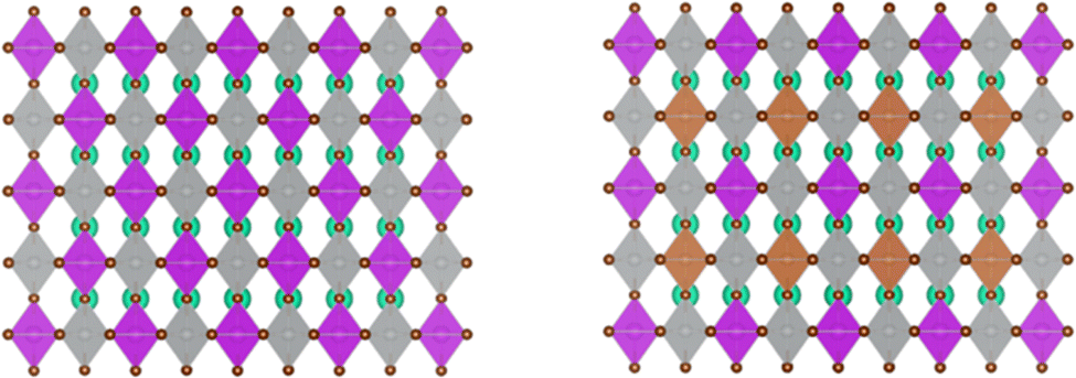
We employed first-principles calculations to investigate the band gap and photoelectric performance of the system after doping with different ratios of Sb. The specific calculation results and analysis process can be found in the ESI.† By comparing the results, we hypothesize that doping Bi in the original system with a ratio of 0.375 Sb will be more beneficial for improving the photoelectric conversion efficiency of Cs2AgBiBr6. This study established a 2 × 2 × 2 Cs2AgBiBr6 perovskite supercell comprising 320 atoms, with Ag and Bi atoms alternately arranged in three dimensions, as depicted in Fig. 1(a). For the doping sites, we chose high-symmetry points. The specific doping method involved interlayer substitution on the xz plane of the Cs2AgBiBr6 supercell, where 3/4 of the Bi atoms were replaced by Sb, resulting in a 2 × 2 × 2 Cs2AgSb0.375Bi0.625Br6 supercell, as depicted in Fig. 1(b). This doping method minimizes structural disruption, maintaining overall material stability. At the same time, high-symmetry sites also play a crucial role in the band structure and help reduce lattice scattering. Previous studies have shown that doping at high-symmetry points can effectively improve the performance of perovskite materials.38,54,55 After doping using this method, we performed geometric optimization and static calculations; the alloyed supercell is shown in Fig. 2. We found that structural changes were minimal, with negligible cell deformation, bond lengths even shortening, ionic binding energy decreasing, and crystallographic parameters remaining stable. The deformation caused by alloying was within 0.35%, and there was a trend of cell volume reduction. From a thermodynamic perspective, alloying can occur spontaneously in nature. Fig. S4 (ESI†) presents perspective views of the pristine Cs2AgBiBr6 system and the doped Cs2AgSb0.375Bi0.625Br6 system in various directions. | ||
| Fig. 1 Crystalline structures of (a) Cs2AgBiBr6 and (b) Cs2AgSb0.375Bi0.625Br6. | ||
 | ||
| Fig. 2 Cs2AgBixSb1−xBr6 alloying solute Bi–Sb ratio diagram. | ||
Fig. 3 illustrates the cell models of the (a) pristine Cs2AgBiBr6 and (b) Sb-doped Cs2AgSb0.375Bi0.625Br6 systems after geometric optimization at 0 K and 300 K. At low temperatures, the alloyed sample exhibited minimal deviation from the pristine sample after structural optimization. However, following a thermal bath at 300 K, significant differences arose in the octahedral structures of the two distinct cells. The pristine cell maintained a stable inorganic framework, with only slight adjustments in the geometric structure upon heating. In contrast, the Sb-doped system experienced substantial lattice distortion due to the introduction of smaller Sb ions compared to Bi ions. Fig. S5 (ESI†) shows the local octahedral structure configurations of the two cells at room temperature.
 | ||
| Fig. 3 Optimized geometric structures of (a) pristine Cs2AgBiBr6 and (b) Sb-doped Cs2AgSb0.375Bi0.625Br6 at 0 K and 300 K. | ||
To quantitatively describe the effect of Sb element doping on the geometry of double perovskites, we calculated the average bond lengths of the original and doped systems at 0 K and 300 K, as shown in Table 1. At 0 K, the average Bi–Br and Ag–Br bond lengths in Cs2AgBiBr6 are 2.877 Å and 2.834 Å, respectively. At 300 K, due to thermal effects, the average bond lengths of Bi–Br and Ag–Br extend to 2.904 Å and 2.873 Å. After Sb doping, the average bond lengths of Bi–Br and Ag–Br increase from 2.875 Å and 2.835 Å at 0 K to 2.903 Å and 2.873 Å at 300 K. Under thermal effects, the average Bi–Br and Ag–Br bond lengths in the original system increase by 0.027 Å and 0.039 Å, respectively, while in the doped system, they increase by 0.028 Å and 0.038 Å.
| Pristine | Doped | ||||
|---|---|---|---|---|---|
| Bi–Br | Ag–Br | Bi–Br | Ag–Br | Sb–Br | |
| 0 K | 2.877 | 2.834 | 2.875 | 2.835 | 2.822 |
| 300 K | 2.904 | 2.873 | 2.903 | 2.873 | 2.855 |
| Increase | 0.027 | 0.039 | 0.028 | 0.038 | 0.033 |
In addition to bond lengths, we also calculated the average Br–Bi–Br bond angles and Br–Ag–Br bond angles of the original and Sb-doped systems at 300 K, as shown in Table 2. The results show that both the Br–Bi–Br bond angle and Br–Ag–Br bond angle in Cs2AgSb0.375Bi0.625Br6 (144.04°, 143.28°) are smaller than those in Cs2AgBiBr6 (144.66°, 143.84°). Angles closer to the ideal 180° indicate weaker distortion of the shape. These results suggest that with the addition of Sb, bond lengths increase and bond angles decrease. The incorporation of Sb increases geometric distortion, enhances atomic disorder, increases atomic motion, and promotes atomic fluctuations.
| Pristine | Doped | ||||
|---|---|---|---|---|---|
| Br–Bi–Br | Br–Ag–Br | Br–Bi–Br | Br–Ag–Br | Br–Sb–Br | |
| 0 K | 180 | 180 | 180 | 180 | 180 |
| 300 K | 144.66 | 143.84 | 144.04 | 143.28 | 143.88 |
| Increase | 35.34 | 36.16 | 35.96 | 36.72 | 36.12 |
The migration and transport of carriers in double perovskites are closely related to the octahedral cage structure rather than the ions of a particular element. Therefore, the changes in the electronic structure brought about by Sb doping are not easily detected in traditional bandgap engineering. We used the Lobster software to calculate the pCOHP for analyzing bonding characteristics, as shown in Fig. 4. Fig. 4(a) illustrates that the conduction band minimum (CBM) of the pristine cell is mainly contributed by the Bi–Br bonds, while the VBM is primarily contributed by the Ag–Br bonds. Fig. 4(b) demonstrates that the contribution of the Sb–Br bonds after doping is significantly higher than that of the other two types of bonds. The results indicate that the VBM is elevated compared to the pristine cell Fermi level, with a shift of approximately 0.2 eV, reducing the bandgap from 1.27 eV to 0.97 eV, which is more favorable for light absorption.
 | ||
| Fig. 4 Crystal orbital Hamilton populations (COHP) of (a) Cs2AgBiBr6 and (b) Cs2AgSb0.375Bi0.625Br6. | ||
The strength of non-adiabatic (NA) electron–phonon coupling is related to the overlap between the highest occupied molecular orbital (HOMO) and the lowest unoccupied molecular orbital (LUMO) wave functions. The matrix element between them is expressed as −iℏ〈φi|∇RH|φj〉, where φi and φj are the wave functions corresponding to the two orbitals. The formula for NAC is as follows:

Here, Ei and Ej are the energies of the two orbitals and Ej − Ei is the corresponding energy gap. H is the Kohn–Sham Hamiltonian and dR/dt represents the nuclear velocity.56 It can be seen that smaller overlap between HOMO and LUMO, a larger energy gap, and smaller nuclear velocity result in smaller NAC, which has a positive effect on the extension of carrier lifetime.
Fig. 5 illustrates the charge density of the HOMO and LUMO for both samples. In the pristine Cs2AgBiBr6 cell, the charge density of the HOMO primarily resides on the Br atoms, while the charge density of the LUMO is mainly concentrated on the Bi atoms, followed by the Br atoms. After Sb doping in the Cs2AgSb0.375Bi0.625Br6 lattice, the charge distribution on the LUMO orbitals tends to localize on the Sb and Br atoms, while the charge density on the Br atoms in the HOMO orbitals gradually delocalizes. The overlap of charge density distributions between LUMO and HOMO was reduced after alloying, thereby decreasing the nonadiabatic coupling (NAC). The nuclear velocity is mainly related to temperature and atomic mass, both of which do not change significantly. The reduced overlap between the wave functions of LUMO and HOMO contributes to the reduction of NAC, whereas the increased band gap after alloying has a suppressing effect on reducing NAC. Between these two factors, the former plays a dominant role. Ultimately, the NAC of the system decreases after alloying. The calculated non-adiabatic coupling values are shown in Table 3. Fig. S6 (ESI†) provides three-dimensional charge isodensity surface imaging.
 | ||
| Fig. 5 Charge densities of the HOMO and LUMO in the (a) pristine Cs2AgBiBr6 and (b) Sb-doped Cs2AgSb0.375Bi0.625Br6. | ||
| Pristine | Doped | |
|---|---|---|
| Initial–ground | Initial–ground | |
| Dephasing (fs) | 30.4 | 22.7 |
| |NAC| (10−6 eV) | 105.8 | 13.7 |
To identify the phonon modes involved in charge trapping and recombination dynamics, we performed a Fourier transform (FT) of the non-normalized autocorrelation function (un-ACF) of CBM–VBM band gap fluctuations to obtain the spectral density.57 As shown in Fig. 6, low-frequency phonon modes play a major role in both the original and doped systems, as they generate non-adiabatic coupling and drive non-radiative electron–hole recombination. Phonon modes below 40 cm−1 dominate the electron–hole recombination process. When the spectral signals of both the original and doped systems are distributed in regions below 40 cm−1, the doped system exhibits higher-frequency vibration modes overall compared to the original system. This is due to the introduction of Sb elements, forming Sb–Br bonds, which fluctuate most intensely, further enhancing the motion of the double perovskite lattice. This influences the selection rules of electron–vibration coupling, activating new high-frequency vibration modes. The introduction of new high-frequency phonon modes accelerates the decoherence process, facilitating the prolongation of the charge recombination process.
 | ||
| Fig. 6 The spectral density of the original and doped systems obtained by the Fourier transform of the energy gap fluctuation autocorrelation function. | ||
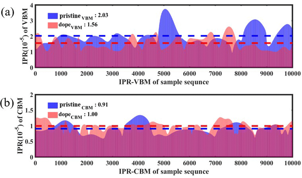
To further characterize the impact of alloying on the charge distribution of key electronic states, we calculated the inverse participation ratio (IPR) of the VBM and CBM over a 10 ps MD trajectory at 300 K. The IPR is an important parameter for calculating the orbital space probability amplitude,

0 < IPR ≤ 1, where N represents the sum of the total grid points in the plane wave basis in the Kohn–Sham equation and ki represents the charge density contributed by electronic state i.58,59 By computing the IPR sequences, the localization degree of the wave function in a certain state can be obtained. A larger IPR value indicates a more localized wave function. IPR = 1 indicates a fully localized state. Fig. 7(a) and (b) respectively show the comparison of the IPR at the VBM and CBM for the pristine Cs2AgBiBr6 sample and the alloyed sample Cs2AgSb0.375Bi0.625Br6. In these figures, blue represents the pristine sample, pink represents the sample after alloying, and purple indicates the overlapping parts. From Fig. 7(b), it can be observed that the change in IPR at the CBM can be almost negligible. However, in Fig. 7(a), the average IPR of the VBM after alloying increased by approximately 1.3 times compared to the pristine sample, indicating a high degree of localization of the VBM wave function. The high localization of electronic states facilitates effective separation of electrons and holes, thereby weakening NAC.
 | ||
| Fig. 7 Comparison of the IPR sequences at the (a) VBM and (b) CBM between the pristine sample and the doped sample. | ||
Finally, we simulated the capture and recombination processes of carriers between different states using the DISH method, obtaining the decay process of the excited-state carriers. We fitted the relaxation curve with an exponential function to obtain a smooth curve, where equilibrium was reached at infinity, and 98% of the equilibrium distribution was considered the end of relaxation. The results are shown in Fig. 8, with the unfitted images displayed in Fig. S7 (ESI†). Fig. 8(a) and (b) depict the evolution curves of electrons and holes in different states for the pristine sample, while Fig. 8(c) and (d) show the evolution curves of electrons and holes for the doped sample. According to the previous analysis in this paper, the lifetime of holes is the main factor determining the carrier lifetime of the system we are studying. When exposed to light, electrons and holes separate, and the holes absorb the photon's energy and are excited to the valence band. Due to the randomness of energy level transitions, holes may occupy different energy levels in the valence band. Studying only one of these states does not provide a comprehensive understanding, and the probability of transitions to energy levels deeper than the deep state is relatively low. Therefore, to ensure more accurate, rigorous, and comprehensive results, we studied three representative states in the valence band. Electrons transition from the initial state to the ground state, while holes transition from the initial state to the other three states (initial state, shallow state and deep state). Comparing Fig. 8(a) and (b), it can be observed that the lifetimes of electrons and holes differ by an order of magnitude. When surplus electrons accumulate net charges at the two poles of the battery material, forming a saturated drift field, the excess electrons annihilate through non-radiative recombination involving mutual repulsion. According to previous studies, holes, as minority carriers in the Cs2AgBiBr6 system, play a major role in determining carrier lifetime.60,61 Therefore, in the samples constructed in this study, we primarily consider the evolution of hole populations. We investigated three representative states in the valence band: the initial state, shallow state, and deep state. As for the electrons, which do not play a major role, their lifetime is mainly related to recombination with holes in the ground state. However, carriers may dwell in shallow and deep energy states, but these states are merely transitional during the relaxation process. In most cases, electron–hole recombination occurs in the ground state, so we mainly compare the recombination time of carriers in the ground state. As shown in Fig. 8(b) and (d), the relaxation process in the pristine sample ends before 10 ps, while in the doped sample, the capture time of non-radiative transitions for holes is extended, and the multi-level states only reach equilibrium at 20 ps. Thus, Sb doping significantly slows down the electron–hole recombination, extending the carrier lifetime by 3–4 times.
 | ||
| Fig. 8 Time-dependent orbital population evolution curves of (a) electrons and (b) holes in the pristine sample, and (c) electrons and (d) holes in the doped sample. | ||
The decoherence method can observe the quantum state evolution of microscopic systems, providing physical evidence for particle jumps between potential energy surfaces; the decoherence time corresponding to state α is τα.
 | (1) |
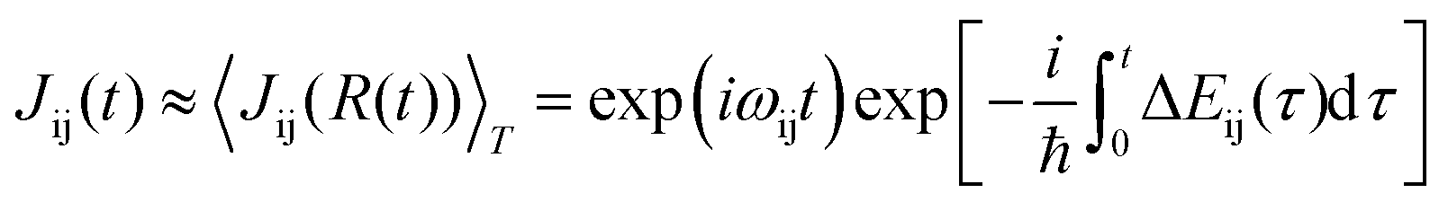 | (2) |
The time-dependent term Jij is the wavepacket overlap of the two-state system, and the environmentally induced decoherence process can be estimated. Zheng Qijing et al. approximated the canonical averaging of the above equation to second-order cumulant terms.
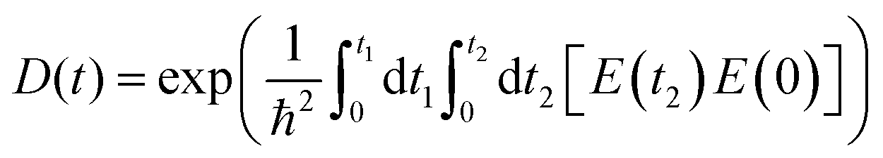 | (3) |
When the response function is obtained by accumulating trajectories according to the above cumulative terms, the characteristic time obtained from fitting a Gaussian function can be considered the decoherence time of the two-state system.
 | (4) |
Meanwhile, the nuclear potential energy acts as the system bath in the quasi-continuous time-dependent evolution, and the NAC vector generated by the two states is part of the time-dependent Hamiltonian evolution.52,62,63
Table 3 provides the decoherence times and NAC coefficients for the electron evolution between the initial and ground states in the pristine Cs2AgBiBr6 system and the Sb-doped system Cs2AgSb0.375Bi0.625Br6. It can be observed that after doping, the decoherence time decreases, and the decoherence rate increases by approximately 1.34 times. Additionally, Sb doping reduces the NAC coefficient by an order of magnitude. While electrons do not predominantly influence the recombination time, alloying still significantly modulates the electron orbitals, which is beneficial for extending the carrier lifetime.
In the dominant thermal hole evolution process, alloying modulation leads to a significant enhancement in the ability to capture carriers by shallow defects. The decoherence time and NAC coefficients for the evolution of holes from the shallow state to the deep state and ground state in the pristine Cs2AgBiBr6 system and the Sb-doped Cs2AgSb0.375Bi0.625Br6 system are shown in Table 4. The relaxation process from the shallow state to the deep state primarily dominates the decoherence time, and after alloying, the decoherence acceleration of hot holes under this pair of energy states is twice that of the pristine sample, greatly hindering the recombination process. In general, a smaller band gap, stronger nonadiabatic coupling, and slower decoherence will lead to faster carrier recombination. After Sb doping, the NAC during the transition from the shallow state to the deep state significantly decreases, indicating an extension of the carrier lifetime. However, there is an opposite trend in NAC when transitioning from the shallow state to the ground state. The final electron–hole recombination time is related to both NAC and decoherence time. We can consider that the reduced decoherence time successfully outweighs the increased NAC. Alloying is an important means of coherence modulation, which can accelerate the decoherence process and delay carrier recombination, and thus extend carrier lifetime.
| Pristine | Doped | |||
|---|---|---|---|---|
| Shallow–deep | Shallow–ground | Shallow–deep | Shallow–ground | |
| Dephasing (fs) | 77.2 | 29.4 | 32.6 | 19.4 |
| |NAC| (10−6 eV) | 2847.5 | 7.12 | 1152.4 | 144.0 |
4. Conclusion
In this study, to elucidate the regulatory mechanism of alloying on the carrier lifetime of the Cs2AgBiBr6 double perovskite, we established the pristine Cs2AgBiBr6 system and an alloying system, Cs2AgSb0.375Bi0.625Br6, by replacing Bi with Sb at a ratio of 0.375. Nonadiabatic molecular dynamics simulations combined with time-dependent density functional theory were employed to systematically investigate the excited-state dynamics of these systems. The results indicate that introducing Sb ions with a smaller radius than Bi ions significantly alters the lattice structure of the double perovskite, changes the intrinsic frequencies of atomic vibrations, and reduces the wave function overlap, thereby lowering the NAC of relevant states. The bandgap of the alloyed sample decreased from 1.27 eV to 0.97 eV, with significant effects on bromine bonds and modification of the conduction band contributed by Bi–Br bonds. Particularly, Sb doping slowed down the hole capture rate and decelerated the non-radiative recombination process of carriers by 3–4 times. The thermalization processes of electrons and holes were presented separately, with electron decoherence increasing by approximately 1.34 times and NAC decreasing. Hole lifetime, which is the bottleneck affecting carrier lifetime, was significantly increased by the alloying method, ultimately effectively extending the carrier lifetime. In summary, this study demonstrates the regulatory effect of alloying on the Cs2AgBiBr6 system, provides compelling evidence for extending carrier lifetime in the Cs2AgSb0.375Bi0.625Br6 sample, and offers suggestions for mitigating harmful defects in Cs2AgBiBr6 double perovskite solar cells.Data availability
All data included in this study are available upon request by contact with the corresponding author.Conflicts of interest
There are no conflicts to declare.References
- D. Shi, V. Adinolfi, R. Comin, M. Yuan, E. Alarousu, A. Buin, Y. Chen, S. Hoogland, A. Rothenberger, K. Katsiev, Y. Losovyj, X. Zhang, P. A. Dowben, O. F. Mohammed, E. H. Sargent and O. M. Bakr, Low trap-state density and long carrier diffusion in organolead trihalide perovskite single crystals, Science, 2015, 347, 519–522 CrossRef CAS PubMed.
- L. Ma, F. Hao, C. C. Stoumpos, B. T. Phelan, M. R. Wasielewski and M. G. Kanatzidis, Carrier Diffusion Lengths of over 500 nm in Lead-Free Perovskite CH3NH3SnI3 Films, J. Am. Chem. Soc., 2016, 138, 14750–14755 CrossRef CAS PubMed.
- W. Liao, D. Zhao, Y. Yu, N. Shrestha, K. Ghimire, C. R. Grice, C. Wang, Y. Xiao, A. J. Cimaroli, R. J. Ellingson, N. J. Podraza, K. Zhu, R.-G. Xiong and Y. Yan, Fabrication of Efficient Low-Bandgap Perovskite Solar Cells by Combining Formamidinium Tin Iodide with Methylammonium Lead Iodide, J. Am. Chem. Soc., 2016, 138, 12360–12363 CrossRef CAS PubMed.
- V. D’Innocenzo, G. Grancini, M. J. P. Alcocer, A. R. S. Kandada, S. D. Stranks, M. M. Lee, G. Lanzani, H. J. Snaith and A. Petrozza, Excitons versus free charges in organo-lead tri-halide perovskites, Nat. Commun., 2014, 5, 3586 CrossRef PubMed.
- H.-S. Kim, C.-R. Lee, J.-H. Im, K.-B. Lee, T. Moehl, A. Marchioro, S.-J. Moon, R. Humphry-Baker, J.-H. Yum, J. E. Moser, M. Grätzel and N.-G. Park, Lead iodide perovskite sensitized all-solid-state submicron thin film mesoscopic solar cell with efficiency exceeding 9%, Sci. Rep., 2012, 2, 591 CrossRef PubMed.
- Z. Liang, Y. Zhang, H. Xu, W. Chen, B. Liu, J. Zhang, H. Zhang, Z. Wang, D.-H. Kang, J. Zeng, X. Gao, Q. Wang, H. Hu, H. Zhou, X. Cai, X. Tian, P. Reiss, B. Xu, T. Kirchartz, Z. Xiao, S. Dai, N.-G. Park, J. Ye and X. Pan, Homogenizing out-of-plane cation composition in perovskite solar cells, Nature, 2023, 624, 557–563 CrossRef CAS.
- M. I. H. Ansari, A. Qurashi and M. K. Nazeeruddin, Frontiers, opportunities, and challenges in perovskite solar cells: A critical review, J. Photochem. Photobiol., C, 2018, 35, 1–24 CrossRef CAS.
- A. Babayigit, A. Ethirajan, M. Muller and B. Conings, Toxicity of organometal halide perovskite solar cells, Nat. Mater., 2016, 15, 247–251 CrossRef CAS PubMed.
- A. E. Shalan, S. Kazim and S. Ahmad, Lead-Free Perovskites: Metals Substitution towards Environmentally Benign Solar Cell Fabrication, ChemSusChem, 2019, 12, 4116–4139 CrossRef CAS PubMed.
- A. Abate, Perovskite Solar Cells Go Lead Free, Joule, 2017, 1, 659–664 CrossRef CAS.
- P. Han and K. Han, Recent Advances in All-Inorganic Lead-Free Three-Dimensional Halide Double Perovskite Nanocrystals, Energy Fuels, 2021, 35, 18871–18887 CrossRef CAS.
- M. R. Filip, S. Hillman, A. A. Haghighirad, H. J. Snaith and F. Giustino, Band Gaps of the Lead-Free Halide Double Perovskites Cs2BiAgCl6 and Cs2BiAgBr6 from Theory and Experiment, J. Phys. Chem. Lett., 2016, 7, 2579–2585 CrossRef CAS PubMed.
- G. Volonakis, M. R. Filip, A. A. Haghighirad, N. Sakai, B. Wenger, H. J. Snaith and F. Giustino, Lead-Free Halide Double Perovskites via Heterovalent Substitution of Noble Metals, J. Phys. Chem. Lett., 2016, 7, 1254–1259 CrossRef CAS PubMed.
- A. H. Slavney, T. Hu, A. M. Lindenberg and H. I. Karunadasa, A Bismuth-Halide Double Perovskite with Long Carrier Recombination Lifetime for Photovoltaic Applications, J. Am. Chem. Soc., 2016, 138, 2138–2141 CrossRef CAS PubMed.
- E. T. McClure, M. R. Ball, W. Windl and P. M. Woodward, Cs2AgBiX6 (X = Br, Cl): New Visible Light Absorbing, Lead-Free Halide Perovskite Semiconductors, Chem. Mater., 2016, 28, 1348–1354 CrossRef CAS.
- R. L. Z. Hoye, L. Eyre, F. Wei, F. Brivio, A. Sadhanala, S. Sun, W. Li, K. H. L. Zhang, J. L. MacManus-Driscoll, P. D. Bristowe, R. H. Friend, A. K. Cheetham and F. Deschler, Fundamental Carrier Lifetime Exceeding 1 μs in Cs2AgBiBr6 Double Perovskite, Adv. Mater. Interfaces, 2018, 5, 1800464 CrossRef.
- V. K. Ravi, N. Singhal and A. Nag, Initiation and future prospects of colloidal metal halide double-perovskite nanocrystals: Cs2AgBiX6 (X = Cl, Br, I), J. Mater. Chem. A, 2018, 6, 21666–21675 RSC.
- Y. Ou, J. Lu, X. Zhong, X. Li, S. Wu, P. Chen and L. Zhou, Efficiency improvement of Cs2AgBiBr6 perovskite solar cells with modification of SnS quantum dots, Mater. Lett., 2022, 312, 131672 CrossRef CAS.
- W. Shockley and H. Queisser, Detailed balance limit of efficiency of p-n junction solar cells, Appl. Phys. Lett., 1961, 510–519 CAS.
- M. Born and R. Oppenheimer, Zur Quantentheorie der Molekeln, Ann. Phys., 1927, 389, 457–484 CrossRef.
- Z. Zhen-Fa, J. Xiang, C. Wei-Bin, Z. Li-Li, G. Hong-Li, Z. Chuan-Yu, W. Ya-Nan, W. Ao-Lei, Z. Qi-Jing and Z. Jin, Investigation of ab initio nonadiabatic molecular dynamics of excited carriers in condensed matter systems, Acta Phys. Sin., 2021, 70, 177101 CrossRef.
- Q. Zheng, W. Chu, C. Zhao, L. Zhang, H. Guo, Y. Wang, X. Jiang and J. Zhao, Ab initio nonadiabatic molecular dynamics investigations on the excited carriers in condensed matter systems, Wiley Interdiscip. Rev.: Comput. Mol. Sci., 2019, 9, e1411 CAS.
- L. Qiao, W.-H. Fang, R. Long and O. V. Prezhdo, Photoinduced Dynamics of Charge Carriers in Metal Halide Perovskites from an Atomistic Perspective, J. Phys. Chem. Lett., 2020, 11, 7066–7082 CrossRef CAS PubMed.
- W. Li, Y. She, A. S. Vasenko and O. V. Prezhdo, Ab initio nonadiabatic molecular dynamics of charge carriers in metal halide perovskites, Nanoscale, 2021, 13, 10239–10265 RSC.
- H. E. Jinlu, L. Run and F. Weihai, A-site Cation Effects on Hot Carrier Relaxation in Perovskites by Nonadiabatic Molecular Dynamics Simulations, Chem. J. Chin. Univ., 2020, 41, 439 Search PubMed.
- R. Shi and R. Long, Atomic Model for Alkali Metal-Doped Tin–Lead Mixed Perovskites: Insight from Quantum Dynamics, J. Phys. Chem. Lett., 2023, 14, 2878–2885 CrossRef CAS.
- C.-J. Tong, L. Li, L.-M. Liu and O. V. Prezhdo, Long Carrier Lifetimes in PbI2-Rich Perovskites Rationalized by Ab Initio Nonadiabatic Molecular Dynamics, ACS Energy Lett., 2018, 3, 1868–1874 CrossRef CAS.
- Z. Zhang and R. Long, Doping-Induced Rapid Decoherence Suppresses Charge Recombination in Mono/Divalent Cation Mixed Perovskites from Nonadiabatic Molecular Dynamics Simulation, J. Phys. Chem. Lett., 2019, 10, 3433–3439 CrossRef CAS PubMed.
- J. Su, Q. Zheng, Y. Shi and J. Zhao, Interlayer Polarization Explains Slow Charge Recombination in Two-Dimensional Halide Perovskites by Nonadiabatic Molecular Dynamics Simulation, J. Phys. Chem. Lett., 2020, 11, 9032–9037 CrossRef CAS PubMed.
- J. Jankowska and O. V. Prezhdo, Ferroelectric Alignment of Organic Cations Inhibits Nonradiative Electron-Hole Recombination in Hybrid Perovskites: Ab Initio Nonadiabatic Molecular Dynamics, J. Phys. Chem. Lett., 2017, 8, 812–818 CrossRef CAS PubMed.
- Z. Zhang, W.-H. Fang, M. V. Tokina, R. Long and O. V. Prezhdo, Rapid Decoherence Suppresses Charge Recombination in Multi-Layer 2D Halide Perovskites: Time-Domain Ab Initio Analysis, Nano Lett., 2018, 18, 2459–2466 CrossRef CAS.
- Y. She, Z. Hou, O. V. Prezhdo and W. Li, Identifying and Passivating Killer Defects in Pb-Free Double Cs2AgBiBr6 Perovskite, J. Phys. Chem. Lett., 2021, 12, 10581–10588 CrossRef CAS PubMed.
- F. Valadares, I. Guilhon, L. K. Teles and M. Marques, Tunable Band Gap and Rhombohedral Distortion in Lead-Free CsSn1–xGexI3 Mixed Perovskites, J. Phys. Chem. C, 2021, 125, 21740–21747 CrossRef CAS.
- W.-J. Yin, Y. Yan and S.-H. Wei, Anomalous Alloy Properties in Mixed Halide Perovskites, J. Phys. Chem. Lett., 2014, 5, 3625–3631 CrossRef CAS PubMed.
- M.-H. Shang, J. Zhang, P. Zhang, Z. Yang, J. Zheng, M. A. Haque, W. Yang, S.-H. Wei and T. Wu, Stable Bandgap-Tunable Hybrid Perovskites with Alloyed Pb–Ba Cations for High-Performance Photovoltaic Applications, J. Phys. Chem. Lett., 2019, 10, 59–66 CrossRef CAS PubMed.
- R. Shi and R. Long, Hole Localization Inhibits Charge Recombination in Tin–Lead Mixed Perovskites: Time–Domain ab Initio Analysis, J. Phys. Chem. Lett., 2019, 10, 6604–6612 CrossRef CAS PubMed.
- J. Liu and O. V. Prezhdo, Chlorine Doping Reduces Electron–Hole Recombination in Lead Iodide Perovskites: Time-Domain Ab Initio Analysis, J. Phys. Chem. Lett., 2015, 6, 4463–4469 CrossRef CAS PubMed.
- E. M. Hutter, M. C. Gélvez-Rueda, D. Bartesaghi, F. C. Grozema and T. J. Savenije, Band-Like Charge Transport in Cs2AgBiBr6 and Mixed Antimony–Bismuth Cs2AgBi1–xSbxBr6 Halide Double Perovskites, ACS Omega, 2018, 3, 11655–11662 CrossRef CAS PubMed.
- G. Kresse and J. Furthmüller, Efficiency of ab-initio total energy calculations for metals and semiconductors using a plane-wave basis set, Comput. Mater. Sci., 1996, 6, 15–50 CrossRef CAS.
- A. Stroppa, P. Barone, P. Jain, J. M. Perez-Mato and S. Picozzi, Hybrid Improper Ferroelectricity in a Multiferroic and Magnetoelectric Metal-Organic Framework, Adv. Mater., 2013, 25, 2284–2290 CrossRef CAS PubMed.
- D. B. Kim, J. Han, Y. S. Jung, K. S. Park, Y. Park, J. Heo and Y. S. Cho, Origin of the anisotropic-strain-driven photoresponse enhancement in inorganic halide-based self-powered flexible photodetectors, Mater. Horiz., 2022, 9, 1207–1215 RSC.
- K. R. Hansen, C. E. McClure, J. S. Colton and L. Whittaker-Brooks, Franz-Keldysh and Stark Effects in Two-Dimensional Metal Halide Perovskites, PRX Energy, 2022, 1, 013001 CrossRef.
- P. E. Blöchl, Projector augmented-wave method, Phys. Rev. B: Condens. Matter Mater. Phys., 1994, 50, 17953–17979 CrossRef PubMed.
- J. P. Perdew, K. Burke and M. Ernzerhof, Generalized Gradient Approximation Made Simple, Phys. Rev. Lett., 1996, 77, 3865–3868 CrossRef CAS PubMed.
- R. Dronskowski and P. E. Bloechl, Crystal orbital Hamilton populations (COHP): energy-resolved visualization of chemical bonding in solids based on density-functional calculations, J. Phys. Chem., 1993, 97, 8617–8624 CrossRef CAS.
- A. Decker, G. A. Landrum and R. Dronskowski, Structural and Electronic Peierls Distortions in the Elements (B): The Antiferromagnetism of Chromium, Z. Anorg. Allg. Chem., 2002, 628, 303–309 CrossRef CAS.
- R. Hoffmann, How Chemistry and Physics Meet in the Solid State, Angew. Chem., Int. Ed. Engl., 1987, 26, 846–878 CrossRef.
- C. F. Craig, W. R. Duncan and O. V. Prezhdo, Trajectory Surface Hopping in the Time-Dependent Kohn-Sham Approach for Electron-Nuclear Dynamics, Phys. Rev. Lett., 2005, 95, 163001 CrossRef PubMed.
- W. Kohn and L. J. Sham, Self-Consistent Equations Including Exchange and Correlation Effects, Phys. Rev., 1965, 140, A1133–A1138 CrossRef.
- Z. Li, X. Zhang and G. Lu, Dipole-Assisted Charge Separation in Organic–Inorganic Hybrid Photovoltaic Heterojunctions: Insight from First-Principles Simulations, J. Phys. Chem. C, 2012, 116, 9845–9851 CrossRef CAS.
- S. A. Fischer, B. F. Habenicht, A. B. Madrid, W. R. Duncan and O. V. Prezhdo, Regarding the validity of the time-dependent Kohn-Sham approach for electron-nuclear dynamics via trajectory surface hopping, J. Chem. Phys., 2011, 134, 024102 CrossRef PubMed.
- H. M. Jaeger, S. Fischer and O. V. Prezhdo, Decoherence-induced surface hopping, J. Chem. Phys., 2012, 137, 22A545 CrossRef PubMed.
- L. Wang, A. Akimov and O. V. Prezhdo, Recent Progress in Surface Hopping: 2011–2015, J. Phys. Chem. Lett., 2016, 7, 2100–2112 CrossRef CAS PubMed.
- M. Righetto, S. Caicedo-Dávila, M. T. Sirtl, V. J.-Y. Lim, J. B. Patel, D. A. Egger, T. Bein and L. M. Herz, Alloying Effects on Charge-Carrier Transport in Silver–Bismuth Double Perovskites, J. Phys. Chem. Lett., 2023, 14, 10340–10347 CrossRef CAS PubMed.
- S. Jiang, M. Liu, D. Zhao, Y. Guo, J. Fu, Y. Lei, Y. Zhang and Z. Zheng, Doping strategies for inorganic lead-free halide perovskite solar cells: progress and challenges, Phys. Chem. Chem. Phys., 2024, 26, 4794–4811 RSC.
- L. Qiao, W.-H. Fang, O. V. Prezhdo and R. Long, Suppressing Oxygen-Induced Deterioration of Metal Halide Perovskites by Alkaline Earth Metal Doping: A Quantum Dynamics Study, J. Am. Chem. Soc., 2022, 144, 5543–5551 CrossRef CAS PubMed.
- A. V. Akimov and O. V. Prezhdo, Persistent Electronic Coherence Despite Rapid Loss of Electron–Nuclear Correlation, J. Phys. Chem. Lett., 2013, 4, 3857–3864 CrossRef CAS.
- J. F. Justo, F. De Brito Mota and A. Fazzio, First-principles investigation of a−SiNx: H, Phys. Rev. B, 2002, 65, 073202 CrossRef.
- S. Ashhab, O. Voznyy, S. Hoogland, E. H. Sargent and M. E. Madjet, Effect of disorder on transport properties in a tight-binding model for lead halide perovskites, Sci. Rep., 2017, 7, 8902 CrossRef CAS PubMed.
- R. E. Brandt, R. C. Kurchin, R. L. Z. Hoye, J. R. Poindexter, M. W. B. Wilson, S. Sulekar, F. Lenahan, P. X. T. Yen, V. Stevanović, J. C. Nino, M. G. Bawendi and T. Buonassisi, Investigation of Bismuth Triiodide (BiI3) for Photovoltaic Applications, J. Phys. Chem. Lett., 2015, 6, 4297–4302 CrossRef CAS PubMed.
- R. Jaramillo, M.-J. Sher, B. K. Ofori-Okai, V. Steinmann, C. Yang, K. Hartman, K. A. Nelson, A. M. Lindenberg, R. G. Gordon and T. Buonassisi, Transient terahertz photoconductivity measurements of minority-carrier lifetime in tin sulfide thin films: Advanced metrology for an early stage photovoltaic material, J. Appl. Phys., 2016, 119, 035101 CrossRef.
- N. Mondal and A. Samanta, Complete ultrafast charge carrier dynamics in photo-excited all-inorganic perovskite nanocrystals (CsPbX3), Nanoscale, 2017, 9, 1878–1885 RSC.
- B. J. Schwartz, E. R. Bittner, O. V. Prezhdo and P. J. Rossky, Quantum decoherence and the isotope effect in condensed phase nonadiabatic molecular dynamics simulations, J. Chem. Phys., 1996, 104, 5942–5955 CrossRef CAS.
Footnotes |
| † Electronic supplementary information (ESI) available. See DOI: https://doi.org/10.1039/d4cp01678e |
| ‡ Yuzhuo Lv, Chang Liu and Yuhang Ma contributed equally to this paper. |
| This journal is © the Owner Societies 2024 |