Enhanced electron transport and optical properties of experimentally synthesized monolayer Si9C15: a comprehensive DFT study for nanoelectronics and photocatalytic applications†
Received
9th April 2024
, Accepted 26th July 2024
First published on 30th July 2024
Abstract
Two-dimensional silicon-carbide (SixCy) materials stand out for their compatibility with current silicon-based technologies, offering unique advantages in nanoelectronics and photocatalysis. In this study, we employ density functional theory and nonequilibrium Green's function methods to investigate the electronic properties, electron transport characteristics, and optoelectronic qualities of experimentally synthesized monolayer Si9C15. Utilizing the modified deformation potential theory formula, we unveil Si9C15's significant directional anisotropy in electron mobility (706.42 cm2 V−1 s−1) compared to holes (432.84 cm2 V−1 s−1) in the a direction. The electrical transport calculations reveal that configurations with a 3 nm channel length demonstrate an ON state when biased, reaching a peak current of 150 nA. Moreover, this maximum current value escalates to 200 nA under tensile strain, marking an increase of approximately 100 times compared to the 5 nm channel, which remains in an OFF state. Si9C15 exhibits high light absorption coefficients (∼105 cm−1) and suitable band edge positions for water splitting at pH 0–7. Applying 1–5% tensile strain can tune the conduction band minimum and valence band maximum closer to the standard redox potentials, enhancing photocatalytic water splitting efficiency. Remarkably, under illumination at pH 0 and 7, Si9C15 can spontaneously catalyze water splitting, demonstrating its potential as a highly efficient photocatalyst. Our findings emphasize the importance of strain control and device length optimization for performance enhancement in nanoelectronics and renewable energy applications, positioning Si9C15 as a promising material for high-performance field-effect transistors and photocatalytic water splitting.
Introduction
In recent years, the push for better electronic device performance has highlighted the potential of two-dimensional (2D) semiconductors in applications like field-effect transistors (FETs) and photocatalysis.1–15 However, despite their promise, limitations such as low mobility, susceptibility to oxidation, and unsuitable bandgap ranges pose significant barriers to broader applications, especially in FETs and photocatalytic water splitting.16 Specifically, the limited mobility of TMDs like MoS2 restricts their efficiency in high-speed electronics,17–19 while phosphorene's propensity for oxidation undermines its long-term stability.15,20–22 Moreover, the narrow bandgaps of materials like silicene and germanene curtail their effectiveness, particularly as the substantial misalignment between their band edges and the hydrogen or oxygen evolution potentials leads to reduced catalytic efficiency in energy-related applications.23–26 These challenges call for the exploration of new materials to overcome existing limitations.
In this context, silicon-carbide (SixCy) materials (x and y represent the relative content or stoichiometric ratio of silicon and carbon atoms, respectively) with their unique advantages, especially their high compatibility with existing silicon-based semiconductor technology, have shown significant research and application value.27 This compatibility not only allows for the easier integration of silicon-carbide materials into existing silicon-based fabrication processes but also significantly reduces the research and development costs and complexity of new devices, accelerating the transition from laboratory to market. The development of SixCy materials not only highlights compatibility with existing silicon-based technology but also, due to their inherent electronic and optical property diversity, research indicates that SixCy, depending on the chemical stoichiometry and type of bonding, can be semiconductors, insulators, or semimetals with a variety of electronic and optical properties.27 For instance, 2D monolayer SiC, with its wide bandgap of 2.56 eV28 achieved through chemical vapor deposition (CVD) and ultrasonication methods, has become a leading material for high-power electronics and high-temperature applications;29,30 g-SiC2, with a bandgap of 1.1 eV,27 shows potential for optoelectronic applications; likewise, variants such as SiC3, Si3C, SiC2, and SiC7, with predicted bandgaps ranging from 0.5 to 3 eV, are anticipated to find broad applications in electronic and optoelectronic devices.27,31 Overall, SixCy and its related structures, due to their excellent performance and broad application prospects, are considered key materials for advancing future semiconductor technology. Gao et al. recently synthesized high-quality monolayer Si9C15 with a honeycomb structure on Ru(0001) and Rh(111) substrates on a large scale. This material exhibited a bandgap of approximately 1.9 eV, indicating distinct semiconductor properties.32 Through a high-temperature reaction process applied to graphene, they transformed it into a dynamically stable Si9C15 layer, elucidating its formation mechanism. Si9C15 demonstrated remarkable environmental stability, retaining its lattice structure and electronic properties with minimal changes even after 72 hours of exposure to air. The potential applications of atomic monolayer Si9C15 are diverse, including in nanoelectronics, nanophotonic, and other advanced technological fields. Its exceptional properties make it a promising candidate for developing new functional materials and devices in areas such as sensors, catalysis, and energy storage.
In addition, researchers are not only focused on discovering new 2D materials but are also committed to changing and optimizing the performance of existing 2D materials through methods such as applying strain,33–35 forming heterostructures,11,36,37 doping with n-type or p-type dopants,38–41 and introducing atomic defects.42–44 Applying strain, as one of these methods, has been proven to be an effective means of controlling the bandgap, expanding the application prospects of 2D semiconductors in nanoelectronics and optoelectronic devices.45,46 For silicon-carbide materials like Si9C15, studying the changes in their electronic properties under the influence of strain is crucial for improving their performance in FET current switch ratio, light absorption coefficient, and photocatalytic water-splitting efficiency. Such studies not only deepen our understanding of the physical behaviours of SixCy materials but also lay the foundation for designing and developing new types of 2D semiconductor devices with enhanced performance, promoting the importance of SixCy and related structures in future applications in electronics and optoelectronics.
In this study, we investigate the electronic properties, electron transport characteristics, and optoelectronic properties of Si9C15, an emerging 2D semiconductor material. Using density functional theory (DFT) and nonequilibrium Green's function (NEGF) methods, we confirm the direct bandgap of Si9C15 to be 1.84 eV as calculated by the Perdew–Burke–Ernzerhof (PBE) method and 2.54 eV according to the Heyd–Scuseria–Ernzerhof (HSE06) approach, consistent with both experimental data and previous theoretical estimates. In order to better predict the carrier mobility of monolayer Si9C15, we utilized the modified deformation potential (DP) theory formula introduced by Lang et al.47 This enhanced formula considers additional factors like carrier scattering mechanisms and phonon vibration modes, resulting in more accurate calculation results compared to the traditional DP formula. We reveal Si9C15's pronounced directional anisotropy in electron mobility, notably higher in the a direction (706.42 cm2 V−1 s−1) than for holes (432.84 cm2 V−1 s−1). The electrical transport calculations reveal that configurations with a 3 nm channel length (Lc) demonstrate an ON state when biased, reaching a peak current of 150 nA. Moreover, this maximum current value escalates to 200 nA under tensile strain, marking an increase of approximately 100 times compared to the 5 nm channel, which remains in an OFF state. Furthermore, Si9C15 exhibits high light absorption coefficients (∼105 cm−1) and suitable band edge positions for water splitting at pH 0–7. Applying 1–5% tensile strain can tune the conduction band minimum (CBM) and valence band maximum (VBM) closer to the standard redox potentials, enhancing photocatalytic water splitting efficiency. Remarkably, under illumination at pH values of 0 and 7, Si9C15 can spontaneously catalyze water splitting, highlighting its potential as a highly efficient photocatalyst. Our findings emphasize the importance of strain control and device dimension optimization for performance enhancement in nanoelectronics and renewable energy applications, positioning Si9C15 as a promising material for high-performance FETs and photocatalytic water splitting.
Calculational method
Details of structure optimization and electronic structure
The geometric optimization and electronic structure calculations of monolayer Si9C15 were carried out on QuantumATK software (version S-2021.06-SP1)48 based on DFT. The PBE functional accurately predicts structural parameters and provides precise geometric structures for various materials. Therefore, in the geometry optimization calculations, the PBE was utilized, employing the linear combination of atomic orbitals (LCAO) method and substituting the full atomic electron potential with PseudoDojo pseudopotentials. The cutoff energy for the real-space density grid was set at 55 Hartree. A 6 × 6 × 1 k-point grid was used to sample the first Brillouin zone. Structural optimization converged when the force on each atom was below 0.01 eV Å−1.
The precise determination of bandgap values is essential for identifying the exact position of the absorption edge in optical absorption spectra and understanding the influence of band edges on photocatalytic efficiency and their response to stress variations. In the study, the HSE06 hybrid functional was employed to enhance the accuracy of electronic structure calculations. A 6 × 6 × 1 k-point grid was utilized to effectively sample the first Brillouin zone while maintaining consistency in the remaining parameters and geometry optimization. This approach, which combines PBE for structure optimization and HSE06 for electronic structure calculations, is a common practice in scientific research.49–51
Given the substantial computational demands of HSE06 calculations compared to PBE and the demonstrated ability of PBE to yield a band gap approximation approaching GW values under heavily doped scenarios in device simulations, the selection of PBE for evaluating electron transport features like carrier mobility52,53 and current–voltage (I–V) characteristics are deemed appropriate.54 In the computation of photocatalytic energy diagrams, the key stages entail optimizing the adsorption geometric structure and evaluating the adsorption energy. The PBE functional is commonly utilized to determine the chemical adsorption energy, delivering credible findings for various photocatalytic systems.55–57 Consequently, the determination of these material properties will rely on the continued use of the PBE functional for electronic structure calculations. The parameters utilized in electronic structure calculations are consistent with those used in geometry optimization.
The calculational method of carrier mobility
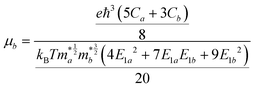
To more accurately predict the carrier mobility of monolayer Si9C15, we employed the modified deformation potential (DP) theory formula proposed by Lang et al.47 Compared with the traditional DP formula, this improved formula takes into account more factors, such as carrier scattering mechanisms and phonon vibration modes, thereby enhancing the reliability of the calculation results. The formula is as follows:| | 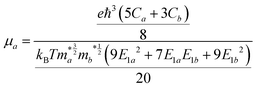 | (1) |
| |  | (2) |
where μa, μb are the carrier mobilities in the a and b directions, respectively, E1a and E1b are the deformation potentials along the a and b directions, m*a and m*b are the effective masses along the a and b directions, T is the temperature, Ca and Cb are the elastic constants in the a and b directions, respectively.
The calculational method of carrier transport properties
We utilized the NEGF method based on DFT, focused on the carrier transport characteristics in the channel region (sub-5 nm). In DFT calculations, Again, the electronic exchange–correlation energies were still described using PBE functional, and PseuDodojo pseudopotentials were employed for calculating carrier transport. To balance computational efficiency with accuracy, the cutoff energy for the real-space density grid was set to 55 Hartree. For sampling in the first Brillouin zone, a 95 × 2 × 1 k-point grid was utilized to compute the I–V characteristic curves in the a direction. The calculation formula for the I−V curves in a two-electrode system are derived from the Landauer–Büttiker formula:58| | 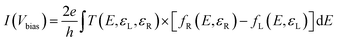 | (3) |
where Vbias is the bias voltage added to both sides of the electrodes and is calculated as: eVbias = εR − εL. εR and εL are the Fermi energy levels of the right and left electrodes, respectively. T represents the carrier transport coefficient, and fL(E, εL) and fR(E, εR) represent the Fermi Dirac distribution of the left and right electrodes, respectively.
Results and discussion
Structural and electronic properties of Si9C15
The structure of monolayer Si9C15, as shown in Fig. 1, consists of a hexagonal primitive cell belonging to the P3 space group. The in-plane lattice parameters are a1 = b1 = 10.02 Å, and the vacuum direction length c is 20 Å. In the structure, Si and C atoms arrange themselves into hexagons in two distinct forms. The first form consists of hexagons with alternating Si and C atoms at their vertices, where the Si–C bond lengths are 1.77 Å and 1.79 Å. The bond angles in the C–Si–C configuration are 116.77°, 125.58°, and 117.29°. The second form comprises hexagons made up of C–C–C and Si–C–Si bonds, with the C–C bond length being 1.50 Å, and the Si–C bond lengths measuring 1.84 Å and 1.79 Å, respectively. All these structural parameters are approximately the same as the previous theoretical calculations.59,60 Previous experiments and theoretical calculations have shown that monolayer Si9C15 is dynamically stable.32,60 To facilitate mobility calculations, we converted the hexagonal primitive cell into an orthogonal cell, shown in Fig. 2, with lattice constants a = 10.02 Å and b = 17.35 Å.
 |
| | Fig. 1 (a) Top view of the hexagonal unit cell, (b) side view of the hexagonal unit cell, (c) orthogonal supercell of Si9C15. | |
 |
| | Fig. 2 Band structure of Si9C15 calculated using the (a) HSE06 functional and (b) PBE functional. The inset in (a) shows the Brillouin zone. | |
As shown in Fig. 2, our calculations indicate that Si9C15 is a direct bandgap semiconductor, with both the CBM and VBM located at the Γ point. The bandgap values are 1.84 eV using the PBE method and 2.54 eV with the HSE06 method. As is well known, PBE suffers from self-interaction error, leading to an underestimation of the band gap, while HSE06 partially corrects this error by introducing a certain proportion of exact exchange. Therefore, HSE06 typically provides more accurate band gap values. The band gap value has a significant impact on the accurate position of the absorption edge in subsequent optical absorption spectra, as well as the band edge position and its variation with stress, which affects the efficiency of photocatalysis. Therefore, these types of calculations and analyses are all based on the electronic structure of HSE06. For electronic transport and photocatalytic step diagram calculations, we use electronic structures based on the PBE functional to balance computational efficiency and accuracy, as stated in the calculational methods section. These findings are also in close proximity to earlier theoretical calculations,59,60 indicating that Si9C15 is a semiconductor with a moderate bandgap. It is noted that the experimentally measured band gap of 1.90 eV was obtained for Si9C15 on Ru(0001) and Rh(111) substrates. The interaction between Si9C15 and the substrate reduces the bandgap of the former. This is because the HSE06 method appears to overestimate the bandgap. It has a bandgap greater than 1.23 eV, making it well-suited for application as a photocatalytic material for water splitting.
Anisotropic carrier mobility
Through calculations, we discovered that Si9C15 exhibits distinctive anisotropy in the direction of carrier mobility (Table 1). In the a direction, the electron mobility significantly surpasses that of holes, reaching 706.42 cm2 V−1 s−1 and 432.84 cm2 V−1 s−1, respectively. This electron mobility not only substantially exceeds that of MoS2 at 23 cm2 V−1 s−1 (ref. 53) and Zr2CO2 at 260 cm2 V−1 s−1 (ref. 47) but also is comparable to Ga2S3 at 657 cm2 V−1 s−1;52 concurrently, its hole mobility surpasses Sc2C(OH)2 at 20 cm2 V−1 s−1 (ref. 47) and is similar to CdPSe3 at 435.7 cm2 V−1 s−1.61 Additionally, in the b direction, the mobilities of electrons and holes are not significantly different, recorded at 475.53 cm2 V−1 s−1 and 436.01 cm2 V−1 s−1, respectively, where the electron mobility exceeds that of GeSSe at 132.31 cm2 V−1 s−1 (ref. 62) and BCN at 128 cm2 V−1 s−1,63 approaching that of GeCH3 at 510 cm2 V−1 s−1;47 while the hole mobility exceeds ZnPSe3 at 310.82 cm2 V−1 s−1 (ref. 64) and GaInS3 at 350 cm2 V−1 s−1,65 nearing BC2N at 390 cm2 V−1 s−1.47 Analyzing from the perspective of carrier types, starting with electrons, the mobility in the a direction is greater than that in the b direction; from the perspective of holes, the mobilities in the a and b directions are similar, indicating anisotropic electron mobility. The difference in carrier mobility between the a and b directions implies that Si9C15 could serve as a directional channel material with selective advantages in designing electronic devices such as FETs. It also offers a new avenue for regulating the separation and mobility of electrons and holes during photocatalytic reactions, potentially enhancing photocatalytic efficiency by optimizing the material's directionality.
Table 1 The deformation potential E1, elastic constant C2D, effective mass m* and carrier mobility μ of Si9C15 were calculated at room temperature 300 K
| Carrier |
E
1 (eV) |
C
2D (N m−1) |
m* (m0) |
μ (cm2 V−1 s−1) |
|
e(a) |
−2.74 |
97.90 |
0.57 |
706.42 |
|
e(b) |
−2.77 |
98.48 |
0.84 |
475.33 |
|
h(a) |
3.15 |
97.90 |
0.70 |
432.84 |
|
h(b) |
3.06 |
98.48 |
0.71 |
436.01 |
Band gap and effective mass response to strain
We subjected monolayer Si9C15 to uniaxial strains ranging from −5% to 5% to observe its bandgap response (Fig. 3). The results demonstrated that the bandgap increases under compressive stress and decreases with tensile strain, irrespective of whether it is in the a or b direction. Notably, under strains from −2% to 2% in the a direction, Si9C15 retained its direct bandgap nature, with the bandgap value adjusting from an unstrained 2.54 eV/1.84 eV (HSE06/PBE) to 2.73 eV/1.95 eV (HSE06/PBE) under −2% compression and to 2.45 eV/1.72 eV under 2% tension (HSE06/PBE); beyond this range of strain, it transitioned to an indirect bandgap, with bandgap values near the Γ point changing by less than 0.15 eV (Eig < Edg < Eig + 0.15 eV).66 In the b direction, similar maintenance of the direct bandgap was observed for strains from −4% to 2%, with the bandgap value shifting from an unstrained 2.54 eV/1.84 eV (HSE06/PBE) to 2.75 eV/2.00 eV under −4% compression and to 2.40 eV/1.72 eV(HSE06/PBE) under 2% tension respectively; when the strain in the b direction exceeded this range, Si9C15 also exhibited an indirect bandgap, with values concentrated near the Γ point, but the change was no more than 0.15 eV (Eig < Edg < Eig + 0.15 eV). The modulation of the bandgap with applied uniaxial strain from −5% to 5% not only highlights the tunability of Si9C15 but also offers new pathways for performance optimization in potential applications. For FETs, the strain-induced bandgap enlargement could enhance the switch ratio and reduce leakage currents, thereby lowering power consumption, which is beneficial for high-performance and low-energy electronic devices. Conversely, a reduction in the bandgap may lower the threshold voltage, essential for applications requiring rapid switching and high conductivity. Regarding photocatalytic performance, the bandgap adjustment affects Si9C15's light absorption range. A decrease in the bandgap, especially an extension into the visible light region, can enhance material utilization of light energy, thereby improving the efficiency of photocatalytic water splitting. While an increased bandgap might limit visible light absorption, for certain photocatalytic reactions, a larger bandgap can enhance selectivity or stability. Thus, by controlling the strain applied to Si9C15, not only can its bandgap be precisely tuned to meet different application needs, but this property can also be leveraged to optimize the electronic performance of FETs or enhance the efficiency and selectivity of photocatalytic processes.
 |
| | Fig. 3 The bandgap variation of Si9C15 after applying −5% to 5% strain along the (a) a direction and (b) b direction, where the white and orange regions represent the strain ranges corresponding to direct and quasi-direct bandgaps, respectively. | |
As shown in Fig. 4, when tensile strain is applied in the a direction, the electron effective mass  undergoes an initial increase followed by a decrease, changing from 0.57 m0 to 0.73 m0 and finally dropping to 0.42 m0, while the hole effective mass
  continuously decreases from 0.70 m0 to 0.50 m0. The application of compressive strain in a direction initially leads to a reduction in the
  to 0.39 m0, followed by an increase to approximately 0.50 m0, whereas the
  increases from 0.70 m0 to 1.50 m0 before finally reducing to 1.16 m0. In the b direction, tensile strain leads to a fluctuation in the
  from 0.84 m0 to 0.55 m0, while the
  varies from 0.71 m0 to around 0.61 m0. Under compressive strain, the
  changes from 0.84 m0 to 0.50 m0, and the
  experiences a variation from 1.59 m0 to 0.77 m0. For electronic devices such as FETs, a smaller effective mass m* is advantageous. Therefore, in FET applications, especially those pursuing high current densities and fast response times, the reduction of m* in Si9C15 along specific directions (e.g., the a direction) is generally considered a favorable change for enhancing device performance. However, in photocatalytic applications, the impact of m* changes in performance are more complex. Smaller m* can accelerate the separation and migration of photogenerated charge carriers, potentially improving photocatalytic efficiency. Nevertheless, in some cases, larger m* may help increase the localization ability of charge carriers, reduce carrier recombination, and thus enhance the material's utilization of light energy and boost photocatalytic activity. Consequently, the tuning of m* in Si9C15 offers the possibility to optimize specific photocatalytic reactions by precisely controlling its electronic and photoelectric properties.
 |
| | Fig. 4 The effect of strain along a and b direction on the effective masses of electrons  and holes and holes  in Si9C15. in Si9C15. | |
Anisotropic I–V characteristics
We calculated the I–V characteristics curves in two-electrode systems of Si9C15 with 3 nm and 5 nm Lc along the a direction. As illustrated in Fig. 5, the two-electrode model employs undoped Si9C15 as the channel and n-type heavily doped Si9C15 as the electrodes, to avoid the influence of factors such as metal–semiconductor contact. To prevent the electrode doping concentration from impacting carrier transport performance, an electron doping concentration of 1.10 × 1014 cm−2 was chosen. This sets the Fermi level of the Si9C15 electrodes 0.16 eV below CBM, fulfilling two main requirements: providing sufficient carriers in both electrodes and achieving experimentally feasible doping concentrations. As depicted in Fig. 6(a), under a bias range of −0.6 V to 0.6 V, the two-electrode system with the 3 nm Lc shows an ON state, with the current increasing to approximately 150 nA at ±0.6 V bias, while the 5 nm one remains in an OFF state, with an ION/IOFF ratio of 102. This aligns with the theoretical understanding that shorter Lc leads to better performance. Furthermore, we analyzed the effect of Lc on current magnitude from the perspective of effective barrier height (ΦB) (Fig. 7). The calculated local density of states (LDOS) indicates that the ΦB = 0.316 eV for a 5 nm channel is higher than ΦB = 0.188 eV for a 3 nm channel. A higher ΦB impedes electron transport, resulting in the 3 nm channel exhibiting an ON state, while the 5 nm channel remains in an OFF state. We then investigated the impact of uniaxial strain on the I–V characteristics in the a direction, this study selected two configurations that maintained a (quasi) direct bandgap with significant bandgap value changes: 5% tensile and 5% compressive strain. The corresponding I–V characteristic results are presented in Fig. 6(b). Under bias conditions from −0.6 V to 0.6 V, a 5% tensile strain in the a direction, reducing the bandgap, increased the current compared to the unstrained state, particularly at 0.6 V bias, where it reached about 200 nA, 1.85 times the unstrained state's current. Conversely, the configuration with a 5% compressive strain in the a direction, leading to an increased bandgap value, exhibited a decrease in current, with the current about 35 nA at a 0.6 V bias being only about 0.29 times that of the unstrained state, which is equivalent to approximately 0.18 times that of the 5% tensile state.
 |
| | Fig. 5 The schematic diagram of two-electrode system with Lc of 5 nm and 3 nm, including (a) the top and (b) the side views of the 5 nm configuration, (c) the top and (d) the side views of the 3 nm configuration. | |
 |
| | Fig. 6 The I–V characteristic curves of Si9C15, including (a) those along the a direction for Lc of 3 nm and 5 nm without applied strain, and (b) those for a Lc of 3 nm along the a direction with applied strains of 5% and −5%. | |
 |
| | Fig. 7 The calculated LDOS for two-electrode configurations with Lc of (a) 3 nm and (b) 5 nm under a bias voltage of 0.4 V. ΦB denotes the effective barrier. | |
Light absorption coefficient
Besides carrier mobility, the optical absorption rate is another key parameter for materials, reflecting their potential applications in optoelectronic devices. The magnetic susceptibility tensor can be calculated using the Kubo–Greenwood formula67 using HSE06 functional:| | 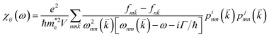 | (4) |
where pnmi〈n![[k with combining right harpoon above (vector)]](https://www.rsc.org/images/entities/i_char_006b_20d1.gif) |
|![[p with combining right harpoon above (vector)]](https://www.rsc.org/images/entities/i_char_0070_20d1.gif) i|m〉 represents the i-th component of the momentum operator between electron states n and m,
i|m〉 represents the i-th component of the momentum operator between electron states n and m,  is the effective mass of the electron. V is the volume, Γ is the energy broadening, fnk is Fermi function. ℏωnm = En − Em signifies the energy difference between the states. The relationship between the relative permittivity εr and the magnetization intensity is given by εr(ω) = 1 + χ(ω). The refractive index n and extinction coefficient κ were calculated from the real (ε1) and imaginary (ε2) parts of the dielectric constant:68
| | 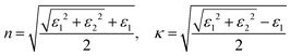 | (5) |
Therefore, the light absorption coefficient can be calculated by the following equation:69
| |  | (6) |
As shown in Fig. 8, under no strain conditions, the absorption coefficient of Si9C15 in the visible and ultraviolet light regions reaches the magnitude of 105 cm−1, comparable to other potential 2D photocatalytic materials. After applying a 5% tensile strain along the a/b direction, which results in a reduced bandgap, there is an observed increase in the maximum absorption coefficient in both the visible and ultraviolet light regions.
 |
| | Fig. 8 The light absorption coefficients of Si9C15 under no strain, when stretched by 5% along the a direction, and when stretched by 5% along the b direction. | |
Photolytic water
The redox capability of photocatalytic water-splitting materials can be assessed by comparing the relative positions of the CBM, VBM, and the redox potentials of water. Therefore, as stated in the Calculational methods section, our calculations and subsequent analysis are based on the electronic structure obtained from the HSE06 functional. An effective catalyst should function across a broad range of pH values. According to the Nernst equation: E(H+/H2) = −4.44 + pH × 0.059 eV, E(O2/H2O) = −5.67 + pH × 0.059 eV,70 the redox potentials at pH = 7 are −4.03 eV for H+/H2 and −5.26 eV for O2/H2O, indicating that the redox potential for water splitting increases with pH value. As illustrated in Fig. 9, without any strain applied, the redox potential for water splitting falls between the CBM and VBM of Si9C15 across pH values from 0 to 7, meeting the requirements for photocatalytic water splitting. Additionally, upon applying uniaxial strain ranging from −5% to +5% in both the a and b directions (excluding +4% and +5% tensile strains in the b direction), Si9C15 continues to meet these photocatalytic requirements by facilitating the reduction and oxidation of water into O2 and H2.
 |
| | Fig. 9 The band edge positions relative to the vacuum energy level of Si9C15 using HSE06. The green and blue dashed lines represent the reduction potential and oxidation potential at pH = 7, 0, respectively. | |
Previous analysis reveals that the closer the positions of the CBM and VBM are to the standard redox potential, the higher the efficiency of water splitting, assuming their bandgap satisfies photocatalytic criteria.71 Fig. S1 (ESI†) shows that applying a uniaxial compressive strain of 0 to −5% in either the a or b direction causes the CBM to shift upwards and the VBM downwards, moving away from the standard redox potential and potentially lowering the efficiency of photocatalytic water splitting. Conversely, applying a uniaxial tensile strain of 0 to +5% in these directions results in a downward shift of the CBM and an upward shift of the VBM, bringing them closer to the standard redox potential. This proximity becomes even more significant as the pH value increases from 0 to 7, suggesting a potential increase in catalytic efficiency for water splitting. Overall, Si9C15 exhibits robust photocatalytic activity within the pH range of 0 to 7, capable of simultaneously producing hydrogen and oxygen gases. Importantly, the efficiency of water splitting catalysis is enhanced under conditions of uniaxial tensile strain in either the a or b direction.
In practical applications, achieving water splitting with photocatalytic materials without the use of sacrificial reagents and co-catalysts presents significant challenges.72,73 Therefore, we conducted an in-depth study on the overall reaction process of water splitting under visible light irradiation, that is, under conditions driven by photogenerated carriers. Based on the free energy theory proposed by Nørskov and others, we calculated the catalytic activity of Si9C15 in different pH environments, including the changes in free energy for the HER and OER processes of water splitting in neutral (pH = 7) and highly acidic (pH = 0) environments, with details provided in the ESI† (eqn (S1)–(S12) and Table S1).74,75
Firstly, we examined the HER reaction (Fig. 10(a)), including the two-step reaction process and electron transfer, described by eqn (S1) and (S2) (ESI†), with the energy change calculations presented in S7 and S8. At pH = 7, with an external potential energy of Ue = 0.77 eV, the free energy changes of the two-electron reaction were ΔG1 = 0.15 eV (endothermic reaction) and ΔG2 = −1.69 eV (exothermic reaction). The barrier for the first step was 0.15 eV, below the spontaneous chemical reaction threshold of 0.2 eV,49,76,77 indicating that the HER reaction can proceed spontaneously under neutral conditions with illumination. At pH = 0 and an external potential energy of Ue = 1.18 eV, the free energy changes for the HER reaction were ΔG1 = −0.26 eV and ΔG2 = −2.10 eV, with the entire process showing a negative energy change, indicating a spontaneous HER reaction.
 |
| | Fig. 10 Free energy diagrams for the (a) two-electron pathways of the HER and (b) four-electron pathways of the OER in the Si9C15 at pH = 0 and 7 and different external potential energy. | |
Next, we evaluated the OER reaction (Fig. 10(b)). The OER proceeds through a four-electron reaction, as shown in eqn (S3) and (S6) (ESI†), with the energy changes calculated using eqn (S9)–(S12) (ESI†). At pH = 7, with external potential energy of Uh = 1.77 eV, the free energy changes for the four-electron reaction process were ΔG1 = −1.67 eV, ΔG2 = −0.9 eV, ΔG3 = −2.06 eV, and ΔG4 = −1.06 eV, with the entire process exhibiting negative energy changes and a downhill trend for the free energy of the intermediate states, indicating that the OER reaction can proceed spontaneously under these conditions. In conditions of pH = 0 and external potential energy of Uh = 1.36 eV, the free energy changes for the OER four-electron reaction process were all negative, showing a downhill trend, indicating an exothermic reaction and that the OER reaction can spontaneously proceed. In summary, Si9C15 can achieve spontaneous complete water splitting under conditions of pH = 0 and 7 with sunlight irradiation without the need for sacrificial reagents and co-catalysts, providing important guidance for the development of efficient photocatalysts for renewable energy.
Conclusions
In conclusion, our comprehensive study using DFT and the NEGF method reveals the remarkable electronic, electrical transport, and photoelectric properties of monolayer Si9C15. The calculated bandgap of 1.84 eV (PBE) and 2.54 eV (HSE06) is consistent with the experimental value of 1.9 eV32 and the previous theoretical value of 1.82 eV (PBE), validating our approach. Si9C15 exhibits significant anisotropy in carrier mobility, with electron mobility (706.42 cm2 V−1 s−1) being much higher than hole mobility (432.84 cm2 V−1 s−1) along the a direction, providing insights for device design. The bandgap can be tuned within the range of 1.72 to 2.00 eV under −5% to 5% strain, while the effective mass of electrons and holes can be modulated within 0.39–1.00 m0 and 0.50–1.59 m0, respectively under strain −4% to 4%, which is crucial for optimizing the performance of FET devices and photocatalytic processes. The electrical transport calculations reveal that configurations with a 3 nm Lc demonstrate an ON state when biased, reaching a peak current of 150 nA. Moreover, this maximum current value escalates to about 200 nA under tensile strain, marking an increase of approximately 100 times compared to the 5nm channel, which remains in an OFF state. Furthermore, Si9C15 exhibits high light absorption coefficients on the order of 105 cm−1, and its band edge positions satisfy the redox potential requirements for water splitting within the pH range of 0 to 7. Applying tensile strains from 1% to 5% can shift the CBM and VBM of Si9C15 closer to the standard redox potentials, enhancing the efficiency of photocatalytic water splitting. Under illumination at pH = 0 and 7, Si9C15 can spontaneously catalyze water splitting. Our strategic use of HSE06 and PBE functionals allows us to balance accuracy and computational efficiency. HSE06 provides accurate electronic structure and bandgap predictions, which are crucial for determining optical absorption spectra and photocatalytic band edge positions. On the other hand, PBE offers reliable results for carrier mobility and transport I–V characteristics, particularly in highly doped electrodes, as well as for photocatalytic step diagrams. This approach ensures robust and comprehensive insights into the material's electronic, transport, and photocatalytic step diagrams while acknowledging the limitations and strengths of each method. Our findings highlight the potential of Si9C15 as a high-performance channel material for FETs and a catalyst for photocatalytic water splitting. Strain engineering allows tuning of its properties, opening up possibilities for advanced nano-electronic devices and sustainable energy applications. Future research should focus on device optimization, stability studies, and practical application exploration to fully harness the potential of Si9C15.
Author contributions
Yuehua Xu: conceptualization (lead); writing – original draft (equal); writing – review and editing (lead). Daqing Li: investigation (lead); visualization (lead); data curation (lead); writing – original draft (equal).
Data availability
The data that support the findings of this study are available from the corresponding author upon reasonable request.
Conflicts of interest
There are no conflicts to declare.
Acknowledgements
Calculations were carried out in the High-Performance Computing Laboratory of Changzhou University and by Hefei Advanced Computing Center.
Notes and references
- J. Jiang, L. Xu, C. Qiu and L.-M. Peng, Ballistic two-dimensional InSe transistors, Nature, 2023, 616(7957), 470–475, DOI:10.1038/s41586-023-05819-w.
- M. Kang, H. B. Jeong, Y. Shim, H.-J. Chai, Y.-S. Kim, M. Choi, A. Ham, C. Park, M.-K. Jo and T. S. Kim,
et al., Layer-Controlled Growth of Single-Crystalline 2D Bi2O2Se Film Driven by Interfacial Reconstruction, ACS Nano, 2024, 18(1), 819–828, DOI:10.1021/acsnano.3c09369.
- C. Dai, Y. Liu and D. Wei, Two-Dimensional Field-Effect Transistor Sensors: The Road toward Commercialization, Chem. Rev., 2022, 122(11), 10319–10392, DOI:10.1021/acs.chemrev.1c00924.
- X. Feng, R. Cheng, L. Yin, Y. Wen, J. Jiang and J. He, Two-Dimensional Oxide Crystals for Device Applications: Challenges and Opportunities, Adv. Mater., 2024, 36(2), 2304708, DOI:10.1002/adma.202304708.
- J. Qu, H. Cheng, H. Lan, B. Zheng, Z. Luo, X. Yang, X. Yi, G. Wu, S. Chen and A. Pan, Space-Confined Growth of Ultrathin P-Type GeTe Nanosheets for Broadband Photodetectors, Small, 2024, 2309391, DOI:10.1002/smll.202309391.
- G. Liu, C. Zhen, Y. Kang, L. Wang and H.-M. Cheng, Unique physicochemical properties of two-dimensional light absorbers facilitating photocatalysis, Chem. Soc. Rev., 2018, 47(16), 6410–6444, 10.1039/C8CS00396C.
- L.-f Hong, R.-t Guo, Y. Yuan, X.-y Ji, Z.-s Li, Z.-d Lin and W.-g Pan, Recent progress of two-dimensional MXenes in photocatalytic applications: a review, Mater. Today Energy, 2020, 18, 100521, DOI:10.1016/j.mtener.2020.100521.
- Y. Chen, P.-M. Wang, Z.-T. Chen and B. Li, Modulating Charge Transfer Pathways to Enhance Photocatalytic Performance of the Metal–Organic Layer Nanosheet, ACS Appl. Mater. Interfaces, 2023, 15(40), 46982–46994, DOI:10.1021/acsami.3c09985.
- Y. Xu, D. Li, H. Sun, H. Xu and P. Li, Comprehensive Understanding of Electron Mobility and Superior Performance in Sub-10 nm DG ML tetrahex-GeC2 n-type MOSFET, Phys. Chem. Chem. Phys., 2024, 26(5), 4284–4297, 10.1039/D3CP05327J.
- Y. Xu, Q. Long, Q. Zeng, D. Li and P. Li, Quaternary 2D monolayer Cu2Cl2Se2Hg2: anisotropic carrier mobility and tunable bandgap for transistor and photocatalytic applications, J. Phys.: Condens. Matter, 2023, 35(39), 395303, DOI:10.1088/1361-648X/ace0ab.
- Y. Xu, D. Li, Q. Zeng, H. Sun and P. Li, Type-II 2D AgBr/SiH van der Waals heterostructures with tunable band edge positions and enhanced optical absorption coefficients for photocatalytic water splitting, RSC Adv., 2023, 13(40), 27676–27685 RSC.
- Y. Xu, Q. Long, D. Li and P. Li, 2D Violet phosphorene with highly anisotropic mobility and its vdW heterojunction design for device applications, Phys. Chem. Chem. Phys., 2022, 24(5), 3379–3385, 10.1039/D1CP04810D.
- W. Wu, D. Li, Y. Xu and X. C. Zeng, Two-Dimensional GeC2 with Tunable Electronic and Carrier Transport Properties and a High Current ON/OFF Ratio, J. Phys. Chem. Lett., 2021, 12(47), 11488–11496, DOI:10.1021/acs.jpclett.1c03477.
- Y. Xu, J. Dai and X. C. Zeng, Al2C Monolayer Sheet and Nanoribbons with Unique Direction-Dependent Acoustic-Phonon-Limited Carrier Mobility and Carrier Polarity, J. Phys. Chem. Lett., 2016, 7(2), 302–307, DOI:10.1021/acs.jpclett.5b02695.
- Y. Xu, J. Dai and X. C. Zeng, Electron-transport properties of few-layer black phosphorus, J. Phys. Chem. Lett., 2015, 6(11), 1996–2002 CrossRef CAS PubMed.
- M. S. Ullah, A. H. B. Yousuf, A. D. Es-Sakhi and M. H. Chowdhury, Analysis of optical and electronic properties of MoS2 for optoelectronics and FET applications, AIP Conf. Proc., 2018, 1957(1), 020001, DOI:10.1063/1.5034320.
- X.-J. Song, L.-C. Xu, H.-F. Bai, Y. Li, Z. Ma, Z. Yang, R. Liu and X. Li, Effects of high-k dielectric environment on the full ballistic transport properties of monolayer MoS2 FETs, J. Appl. Phys., 2017, 121(14), 144505 CrossRef.
- Y. Cai, G. Zhang and Y.-W. Zhang, Polarity-reversed robust carrier mobility in monolayer MoS2 nanoribbons, J. Am. Chem. Soc., 2014, 136(17), 6269–6275 CrossRef CAS PubMed.
- L. Liao, Y.-C. Lin, M. Bao, R. Cheng, J. Bai, Y. Liu, Y. Qu, K. L. Wang, Y. Huang and X. Duan, High-speed graphene transistors with a self-aligned nanowire gate, Nature, 2010, 467(7313), 305–308 CrossRef CAS PubMed.
- L. Li, D. Li, Q. Bai, Y. Wang, C. Li, Y. Shen and H. Uyama, One-step synergistic effect to produce two-dimensional N-doped porous carbon nanosheets with ultrahigh porosity from biomass for high-performance supercapacitors, Energy Fuels, 2023, 37(21), 16942–16950 CrossRef CAS.
- H. Liu, A. T. Neal, Z. Zhu, Z. Luo, X. Xu, D. Tománek and P. D. Ye, Phosphorene: an unexplored 2D semiconductor with a high hole mobility, ACS Nano, 2014, 8(4), 4033–4041 CrossRef CAS PubMed.
- S. Das, W. Zhang, M. Demarteau, A. Hoffmann, M. Dubey and A. Roelofs, Tunable transport gap in phosphorene, Nano Lett., 2014, 14(10), 5733–5739 CrossRef CAS PubMed.
-
M. W. Chuan; K. L. Wong; A. Hamzah; S. Rusli; N. E. Alias; C. S. Lim and M. L. P. Tan, Device performance of silicene nanoribbon field-effect transistor under ballistic transport, in 2020 IEEE International Conference on Semiconductor Electronics (ICSE), IEEE, 2020, pp. 5–8 Search PubMed.
- L. Tao, E. Cinquanta, D. Chiappe, C. Grazianetti, M. Fanciulli, M. Dubey, A. Molle and D. Akinwande, Silicene field-effect transistors operating at room temperature, Nat. Nanotechnol., 2015, 10(3), 227–231 CrossRef CAS PubMed.
-
M. A. Kharadi; G. F. A. Malik; F. A. Khanday and K. A. Shah, Electronic properties of fluorine functionalized germanene nanoribbons, in 2020 IEEE VLSI Device Circuit and System (VLSI DCS), IEEE, 2020, pp. 1–4 Search PubMed.
- S. Kaneko, H. Tsuchiya, Y. Kamakura, N. Mori and M. Ogawa, Theoretical performance estimation of silicene, germanene, and graphene nanoribbon field-effect transistors under ballistic transport, Appl. Phys. Express, 2014, 7(3), 035102 CrossRef CAS.
- Z. Shi, Z. Zhang, A. Kutana and B. I. Yakobson, Predicting two-dimensional silicon carbide monolayers, ACS Nano, 2015, 9(10), 9802–9809 CrossRef CAS PubMed.
- H. Şahin, S. Cahangirov, M. Topsakal, E. Bekaroglu, E. Akturk, R. T. Senger and S. Ciraci, Monolayer honeycomb structures of group-IV elements and III-V binary compounds: First-principles calculations, Phys. Rev. B: Condens. Matter Mater. Phys., 2009, 80(15), 155453 CrossRef.
- S. S. Lin, Light-Emitting Two-Dimensional Ultrathin Silicon Carbide, J. Phys. Chem. C, 2012, 116(6), 3951–3955, DOI:10.1021/jp210536m.
- Z. Huang, N. Lu, Z. Wang, S. Xu, J. Guan and Y. Hu, Large-Scale Ultrafast Strain Engineering of CVD-Grown Two-Dimensional Materials on Strain Self-Limited Deformable Nanostructures toward Enhanced Field-Effect Transistors, Nano Lett., 2022, 22(18), 7734–7741 CrossRef CAS PubMed.
- Y. Ding and Y. Wang, Geometric and electronic structures of two-dimensional SiC3 compound, J. Phys. Chem. C, 2014, 118(8), 4509–4515 CrossRef CAS.
- Z. Y. Gao, W. Xu, Y. Gao, R. Guzman, H. Guo, X. Wang, Q. Zheng, Z. Zhu, Y. Y. Zhang and X. Lin, Experimental Realization of Atomic Monolayer Si9C15, Adv. Mater., 2022, 34(35), 2204779 CrossRef CAS PubMed.
- H. T. T. Nguyen, V. V. Tuan, C. V. Nguyen, H. V. Phuc, H. D. Tong, S.-T. Nguyen and N. N. Hieu, Electronic and optical properties of a Janus SnSSe monolayer: effects of strain and electric field, Phys. Chem. Chem. Phys., 2020, 22(20), 11637–11643 RSC.
- A. Marjaoui, M. A. Tamerd, M. Diani, A. Aouni, M. Ajdour and M. Zanouni, Biaxial strain engineering of the electronic and optical properties of Ge2SeS monolayer: Promising for optoelectronic applications, Comput. Condens. Matter, 2022, 32, e00717 CrossRef.
- X. Li, Z. Li, J. Han, S. Cao and Z. Zhang, Single-layer PtSe2 adsorbed with non-metallic atoms: geometrical, mechanical, electronic and optical properties and strain effects, Phys. Chem. Chem. Phys., 2024, 26(5), 4218–4230 RSC.
- B. Qiu, X. Zhao, G. Hu, W. Yue, J. Ren and X. Yuan, Optical properties of graphene/MoS2 heterostructure: first principles calculations, Nanomaterials, 2018, 8(11), 962 CrossRef PubMed.
- C. V. Nguyen, C. Q. Nguyen, S.-T. Nguyen, Y. S. Ang and N. V. Hieu, Two-dimensional metal/semiconductor contact in a Janus MoSH/MoSi2N4 van der Waals heterostructure, J. Phys. Chem. Lett., 2022, 13(11), 2576–2582 CrossRef CAS PubMed.
- H. A. Elsayed, S. A. El-Naggar and A. H. Aly, Two dimensional tunable photonic crystals and n doped semiconductor materials, Mater. Chem. Phys., 2015, 160, 221–226 CrossRef CAS.
- Z. Liu, T. He, Q. Jiang, W. Wang and J. Tang, A review of heteroatomic doped two-dimensional materials as electrocatalysts for hydrogen evolution reaction, Int. J. Hydrogen Energy, 2022, 47(69), 29698–29729 CrossRef CAS.
- R. Du, Y. Wang, M. Cheng, P. Wang, H. Li, W. Feng, L. Song, J. Shi and J. He, Two-dimensional multiferroic material of metallic p-doped SnSe, Nat. Commun., 2022, 13(1), 6130 CrossRef CAS PubMed.
- J. Cao, J. Zhou, J. Liu, W. Wang, J. Chen, J. Shi, Y. Zhang and X. Liu, Sensing Behavior of Two Dimensional Al-and P-Doped WS2 Toward NO, NO2, and SO2: An Ab Initio Study, Nanoscale Res. Lett., 2020, 15, 1–9 CrossRef PubMed.
- Y. Xie, F. Liang, S. Chi, D. Wang, K. Zhong, H. Yu, H. Zhang, Y. Chen and J. Wang, Defect engineering of MoS2 for room-temperature terahertz photodetection, ACS Appl. Mater. Interfaces, 2020, 12(6), 7351–7357 CrossRef CAS PubMed.
- S. Yang, J. Kang, Q. Yue, J. Coey and C. Jiang, Defect-modulated transistors and gas-enhanced photodetectors on ReS2 nanosheets, Adv. Mater. Interfaces, 2016, 3(6), 1500707 CrossRef.
- C. Cuhadar, S.-G. Kim, J.-M. Yang, J.-Y. Seo, D. Lee and N.-G. Park, All-inorganic bismuth halide perovskite-like materials A3Bi2I9 and A3Bi1.8Na0.2I8.6 (A = Rb and Cs) for low-voltage switching resistive memory, ACS Appl. Mater. Interfaces, 2018, 10(35), 29741–29749 CrossRef CAS PubMed.
- G. G. Naumis, S. Barraza-Lopez, M. Oliva-Leyva and H. Terrones, Electronic and optical properties of strained graphene and other strained 2D materials: a review, Rep. Prog. Phys., 2017, 80(9), 096501 CrossRef PubMed.
- D. Çakır, H. Sahin and F. M. Peeters, Tuning of the electronic and optical properties of single-layer black phosphorus by strain, Phys. Rev. B: Condens. Matter Mater. Phys., 2014, 90(20), 205421 CrossRef.
- H. Lang, S. Zhang and Z. Liu, Mobility anisotropy of two-dimensional semiconductors, Phys. Rev. B, 2016, 94(23), 235306 CrossRef.
- S. Smidstrup, T. Markussen, P. Vancraeyveld, J. Wellendorff, J. Schneider, T. Gunst, B. Verstichel, D. Stradi, P. A. Khomyakov and U. G. Vej-Hansen, QuantumATK: an integrated platform of electronic and atomic-scale modelling tools, J. Phys.: Condens. Matter, 2019, 32(1), 015901 CrossRef PubMed.
- Y. Yu, J. Zhou, Z. Guo and Z. Sun, Novel two-dimensional Janus MoSiGeN4 and WSiGeN4 as highly efficient photocatalysts for spontaneous overall water splitting, ACS Appl. Mater. Interfaces, 2021, 13(24), 28090–28097 CrossRef CAS PubMed.
- Y. Ding and Y. Wang, First-principles study of two-dimensional MoN2X2Y2 (X = B∼In, Y = N∼Te) nanosheets: The III–VI analogues of MoSi2N4 with peculiar electronic and magnetic properties, Appl. Surf. Sci., 2022, 593, 153317 CrossRef CAS.
- Y. Peng, Q. Zhu, W. Xu and J. Cao, High anisotropic optoelectronics in monolayer binary M8X12 (M = Mo, W; X = S, Se, Te), ACS Appl. Mater. Interfaces, 2022, 14(23), 27056–27062 CrossRef CAS PubMed.
- G. Zhang, K. Lu, Y. Wang, H. Wang and Q. Chen, Mechanical and electronic properties of α-M2X3 (M= Ga, In; X= S, Se) monolayers, Phys. Rev. B, 2022, 105(23), 235303 CrossRef CAS.
- A. Rawat, N. Jena and A. De Sarkar, A comprehensive study on carrier mobility and artificial photosynthetic properties in group VI B transition metal dichalcogenide monolayers, J. Mater. Chem. A, 2018, 6(18), 8693–8704 RSC.
- H. Li, P. Xu and J. Lu, Sub-10 nm tunneling field-effect transistors based on monolayer group IV mono-chalcogenides, Nanoscale, 2019, 11(48), 23392–23401 RSC.
- Y. Zhang, L. Xu, B. Liu, X. Wang, T. Wang, X. Xiao, S. Wang and W. Huang, Engineering BiVO4 and Oxygen Evolution Cocatalyst Interfaces with Rapid Hole Extraction for Photoelectrochemical Water Splitting, ACS Catal., 2023, 13(9), 5938–5948, DOI:10.1021/acscatal.3c00444.
- H. Xu, D. Cheng, D. Cao and X. C. Zeng, A universal principle for a rational design of single-atom electrocatalysts, Nat. Catal., 2018, 1(5), 339–348 CrossRef CAS.
- G. Yuan, X. Ma, J. Liao, T. Xie, Q. Xie and Z. Yuan, First-Principles Calculations of 2D Janus WSSiN2 Monolayer for Photocatalytic Water Splitting, ACS Appl. Nano Mater., 2023, 6(3), 1956–1964, DOI:10.1021/acsanm.2c04918.
-
S. Datta, Electronic transport in mesoscopic systems, Cambridge University Press, 1997 Search PubMed.
- Z. Cui, Y. Lyu, R. Li and P. Wu, Adsorption of metals on Si9C15 monolayer for optoelectronic applications, Vacuum, 2023, 217, 112565 CrossRef CAS.
- M. B. Tagani, Si9C15 monolayer: A silicon carbide allotrope with remarkable physical properties, Phys. Rev. B, 2023, 107(8), 085114, DOI:10.1103/PhysRevB.107.085114.
- H. M. Khalil, M. F. Khan, J. Eom and H. Noh, Highly stable and tunable chemical doping of multilayer WS2 field effect transistor: Reduction in contact resistance, ACS Appl. Mater. Interfaces, 2015, 7(42), 23589–23596 CrossRef CAS PubMed.
- P. Nandi, A. Rawat, R. Ahammed, N. Jena and A. De Sarkar, Group-IV(A) Janus dichalcogenide monolayers and their interfaces straddle gigantic shear
and in-plane piezoelectricity, Nanoscale, 2021, 13(10), 5460–5478 RSC.
- B. Mortazavi, F. Shojaei, M. Yagmurcukardes, A. V. Shapeev and X. Zhuang, Anisotropic and outstanding mechanical, thermal conduction, optical, and piezoelectric responses in a novel semiconducting BCN monolayer confirmed by first-principles and machine learning, Carbon, 2022, 200, 500–509 CrossRef CAS.
- A. Kishore, H. Seksaria, A. Arora and A. De Sarkar, Regulating excitonic effects in non-oxide based XPSe3 (X = Cd, Zn) monolayers towards enhanced photocatalysis for overall water splitting, Phys. Chem. Chem. Phys., 2023, 25(30), 20337–20349 RSC.
- W. Chen, H. Yin, S. Jiang, S. Liu, C. Liu, B. Wang and G.-P. Zheng, Anomalous layer-dependent electronic and piezoelectric properties of 2D GaInS3 nanosheets, Appl. Phys. Lett., 2021, 118(21), 213103 CrossRef CAS.
- I.-H. Lee, J. Lee, Y. J. Oh, S. Kim and K.-J. Chang, Computational search for direct band gap silicon crystals, Phys. Rev. B: Condens. Matter Mater. Phys., 2014, 90(11), 115209 CrossRef.
- J. Sipe and E. Ghahramani, Nonlinear optical response of semiconductors in the independent-particle approximation, Phys. Rev. B: Condens. Matter Mater. Phys., 1993, 48(16), 11705 CrossRef CAS PubMed.
-
R. M. Martin, Electronic structure: basic theory and practical methods, Cambridge University Press, 2020 Search PubMed.
-
D. J. Griffiths, Introduction to electrodynamics, Cambridge University Press, 2023 Search PubMed.
- M. M. Walczak, D. A. Dryer, D. D. Jacobson, M. G. Foss and N. T. Flynn, pH dependent redox couple: An illustration of the Nernst equation, J. Chem. Educ., 1997, 74(10), 1195 CrossRef CAS.
- W. Hu, L. Lin, R. Zhang, C. Yang and J. Yang, Highly Efficient Photocatalytic Water Splitting over Edge-Modified Phosphorene Nanoribbons, J. Am. Chem. Soc., 2017, 139(43), 15429–15436, DOI:10.1021/jacs.7b08474.
-
J. Schneider and D. W. Bahnemann, Undesired role of sacrificial reagents in photocatalysis, ACS Publications, 2013, vol. 4, pp. 3479–3483 Search PubMed.
- J. J. Velázquez, R. Fernández-González, L. Díaz, E. P. Melián, V. D. Rodríguez and P. Núñez, Effect of reaction temperature and sacrificial agent on the photocatalytic H2-production of Pt-TiO2, J. Alloys Compd., 2017, 721, 405–410 CrossRef.
- J. K. Nørskov, J. Rossmeisl, A. Logadottir, L. Lindqvist, J. R. Kitchin, T. Bligaard and H. Jonsson, Origin of the overpotential for oxygen reduction at a fuel-cell cathode, J. Phys. Chem. B, 2004, 108(46), 17886–17892 CrossRef.
- Á. Valdés, Z.-W. Qu, G.-J. Kroes, J. Rossmeisl and J. K. Nørskov, Oxidation and photo-oxidation of water on TiO2 surface, J. Phys. Chem. C, 2008, 112(26), 9872–9879 CrossRef.
- Y. Yu, J. Zhou and Z. Sun, Novel 2D Transition-Metal Carbides: Ultrahigh Performance Electrocatalysts for Overall Water Splitting and Oxygen Reduction, Adv. Funct. Mater., 2020, 30(47), 2000570 CrossRef CAS.
- J. K. Nørskov, T. Bligaard, A. Logadottir, J. R. Kitchin, J. G. Chen, S. Pandelov and U. Stimming, Trends in the exchange current for hydrogen evolution, J. Electrochem. Soc., 2005, 152(3), J23 CrossRef.
Footnote |
| † Electronic supplementary information (ESI) available: Fig. S1: evolution of band-edge positions of Si9C15 as a function of applied uniaxial strain in −5% to 5% in the direction a and b, respectively. Eqn (S1)–(S12) OER and HER free energy theory. Table S1 describes the entropy and zero-point energy corrections, which are utilized to determine the free energy of reactants, products, and intermediate species that are adsorbed on catalysts. See DOI: https://doi.org/10.1039/d4cp01456a |
|
| This journal is © the Owner Societies 2024 |
Click here to see how this site uses Cookies. View our privacy policy here. 
 * and
Daqing
Li
* and
Daqing
Li


 undergoes an initial increase followed by a decrease, changing from 0.57 m0 to 0.73 m0 and finally dropping to 0.42 m0, while the hole effective mass
  continuously decreases from 0.70 m0 to 0.50 m0. The application of compressive strain in a direction initially leads to a reduction in the
  to 0.39 m0, followed by an increase to approximately 0.50 m0, whereas the
  increases from 0.70 m0 to 1.50 m0 before finally reducing to 1.16 m0. In the b direction, tensile strain leads to a fluctuation in the
  from 0.84 m0 to 0.55 m0, while the
  varies from 0.71 m0 to around 0.61 m0. Under compressive strain, the
  changes from 0.84 m0 to 0.50 m0, and the
  experiences a variation from 1.59 m0 to 0.77 m0. For electronic devices such as FETs, a smaller effective mass m* is advantageous. Therefore, in FET applications, especially those pursuing high current densities and fast response times, the reduction of m* in Si9C15 along specific directions (e.g., the a direction) is generally considered a favorable change for enhancing device performance. However, in photocatalytic applications, the impact of m* changes in performance are more complex. Smaller m* can accelerate the separation and migration of photogenerated charge carriers, potentially improving photocatalytic efficiency. Nevertheless, in some cases, larger m* may help increase the localization ability of charge carriers, reduce carrier recombination, and thus enhance the material's utilization of light energy and boost photocatalytic activity. Consequently, the tuning of m* in Si9C15 offers the possibility to optimize specific photocatalytic reactions by precisely controlling its electronic and photoelectric properties.
 and holes
  in Si9C15.


 is the effective mass of the electron. V is the volume, Γ is the energy broadening, fnk is Fermi function. ℏωnm = En − Em signifies the energy difference between the states. The relationship between the relative permittivity εr and the magnetization intensity is given by εr(ω) = 1 + χ(ω). The refractive index n and extinction coefficient κ were calculated from the real (ε1) and imaginary (ε2) parts of the dielectric constant:68


