
Thermoelectric properties of Bi1−xPbxCu1−xSeO oxyselenides†
Aleksandra
Khanina
 *a,
Andrei
Novitskii
b,
Daria
Pashkova
b,
Andrei
Voronin
a,
Takao
Mori
bc and
Vladimir
Khovaylo
*ad
*a,
Andrei
Novitskii
b,
Daria
Pashkova
b,
Andrei
Voronin
a,
Takao
Mori
bc and
Vladimir
Khovaylo
*ad
aAcademic Research Center for Energy Efficiency, National University of Science and Technology MISIS, Leninsky Av. 4, Moscow, 119049, Russia. E-mail: khanina.as@misis.ru; khovaylo@misis.ru
bInternational Center for Materials Nanoarchitectonics (WPI-MANA), National Institute for Materials Science (NIMS), 1-1 Namiki, Tsukuba, Ibaraki 305-0044, Japan
cGraduate School of Pure and Applied Sciences, University of Tsukuba, 1-1-1 Tennodai, Tsukuba, Ibaraki 305-8573, Japan
dBelgorod State University, Pobedy St. 85, Belgorod, 308015, Russia
First published on 22nd April 2024
Abstract
In this work, Bi1−xPbxCu1−x SeO (x = 0, 0.02, 0.06, and 0.08) compounds were synthesized by a solid state reaction followed by spark plasma sintering. The effect of simultaneous Bi to Pb substitution and Cu vacancy introduction on thermoelectric properties was investigated systematically. The power factor was significantly enhanced, contributing to the increase in the zT value. As a result, the zTmax of 0.75 at 773 K was obtained for the Bi0.94Pb0.06Cu0.94SeO sample. To reveal the factors constraining the zTmax of Bi1−xPbxCuSeO-based oxyselenides, a further careful analysis of literature data was performed. We highlighted that for Pb-doped oxyselenides, the power factor is almost independent of the synthesis technique, while the lattice thermal conductivity is the main property determining zTmax and is highly affected by the synthesis method.
Introduction
Over the past few decades, global energy consumption has dramatically increased, with about two-thirds of produced energy being lost as waste heat. Therefore, technologies capable of efficiently recovering this heat are crucial for achieving sustainable development goals. In this context, thermoelectric materials, which enable the direct conversion of waste heat into electricity, have attracted significant attention from the scientific community.1 The efficiency of thermoelectric energy conversion depends on the material's transport properties and is determined by the thermoelectric figure of merit zT = α2σT/κtot, where α, σ, T, and κtot represent the Seebeck coefficient, electrical conductivity, absolute temperature, and total thermal conductivity, respectively.2Currently, p-type BiCuSeO-based oxyselenides are among the most efficient oxygen-containing thermoelectric materials.3 BiCuSeO crystallizes in a tetragonal layered ZrCuSiAs structure type with a P4/nmm space group and two formula units per unit cell. The crystal structure consists of alternately stacked insulating (Bi2O2)2+ layers (so-called “charge reservoir” layers) and conducting (Cu2Se2)2− layers along the c-axis.4,5 These BiCuSeO-based oxyselenides have drawn interest as thermoelectric materials, primarily due to their intrinsically low thermal conductivity, not exceeding 1.5 W m−1 K−1 at room temperature, coupled with a relatively high Seebeck coefficient.6 The main purpose of enhancing the zT of BiCuSeO is to optimize the charge carrier concentration n, which significantly boosts the power factor (α2σ) by balancing α and σ values. Employing this approach in BiCuSeO-based oxyselenides has yielded zTmax > 1.2 at T ≥ 773 K, achieved through the substitution of bismuth with various elements.7,8
However, as identified by Ioffe over six decades ago, an efficient thermoelectric material requires not only an optimal charge concentration nopt, but also a maximized ratio of charge carrier mobility μ to lattice thermal conductivity κlat, as this determines the zTmax achievable at a given temperature and charge carrier concentration.2 While optimizing charge carrier concentration in BiCuSeO is feasible through heterovalent Bi substitution, methods to maximize μ/κlat are less straightforward. In this context, it is important to consider the native defect chemistry of p-type BiCuSeO oxyselenides. In particular, copper vacancies (VCu) identified as the predominant defect in BiCuSeO are responsible for its native p-type self-doping.9,10 Moreover, the introduction of extra VCu promotes the carriers' delocalization between the charge reservoir and conducting layers,11,12 which is beneficial for maintaining a high n/μ ratio.13 Although interlayer delocalization of carriers is favorable for interlayer charge transfer, conventional Bi substitution is still necessary to provide a sufficient number of charge carriers for diffusion.14 For this purpose, it makes sense to use the most efficient dopant, Pb,15 which allows one to achieve the highest ratio of the nominal to actual number of introduced charge carriers per atom.
In our study, we synthesized a series of samples with the nominal composition of Bi1−xPbxCu1−xSeO (x = 0, 0.02, 0.06, and 0.08) to achieve simultaneous optimization of charge carrier concentration while maintaining high values of charge carrier mobility by combining the substitution of bismuth with lead (PbBi) and introducing extra copper vacancies (VCu). Bi1−xPbxCuSeO-based oxyselenides are among the most studied compounds, and the influence of Bi to Pb substitution on transport properties has been thoroughly investigated. We demonstrated that the key factor affecting the thermoelectric performance of Pb-doped BiCuSeO and the variability reported in zTmax values is, in fact, the μ/κlat ratio. At the same time, the power factor is predominantly influenced by the PbBi concentration and is weakly dependent on the concentration of vacancies and/or the second dopant. Ultimately, we observed an almost fourfold increase in the power factor for Bi1−xPbxCu1−xSeO with x = 0.06 and 0.08 at 773 K. The μw/κlat ratio doubled with an increase from x = 0 to x = 0.02; however, a further increase in x did not yield an increase in μw/κlat mainly due to the increase in κlat for x > 0.02. Ultimately, a notable increase in zT by a factor of three was realized, and zTmax = 0.75 at 773 K for Bi0.94Pb0.06Cu0.94 SeO was achieved.
Materials and methods
Compounds with the nominal chemical compositions of Bi1−xPbxCu1−xSeO (x = 0, 0.02, 0.06, and 0.08) were synthesized as reported elsewhere16 using high purity CuO, Bi, Se, and PbO powders as the raw materials. The obtained products were consolidated through spark plasma sintering (SPS) at 903 K for 5 min under an axial pressure of 50 MPa. Phase composition analysis was carried out through powder X-ray diffraction (PXRD) using a DRON-3 diffractometer (IC Bourevestnik, Russia) with Cu-Kα radiation (λ = 1.54178 Å). The PXRD patterns were refined by the Rietveld method with the self-developed software package.17 Scanning electron microscopy (SEM) and energy-dispersive X-ray spectroscopy (EDS) were performed using a Vega 3SB SEM (Tescan, Czech Republic) equipped with an x-act EDS detector (Oxford Instruments, UK). The thermal diffusivity χ was measured in the axial direction of disk-shaped samples of ϕ10 × 1 mm2 using a laser flash analyzer (LFA 467 Hyperflash, Netzsch, Germany). The total thermal conductivity κtot was calculated using the formula κtot = χCpd, where Cp represents the specific heat capacity, which was estimated using the comparison method (with Pyroceram-9060 as a reference sample) and is in good agreement with the Cp value calculated by the Debye model. The density d was determined using the Archimedes method. The Seebeck coefficient α and the electrical conductivity σ were measured in the radial direction of bar-shaped specimens with dimensions of 10 × 3 × 1 mm3 using a commercial apparatus (ZEM-3, Advance Riko Inc., Japan) under a partial He atmosphere from 300 to 773 K. The uncertainty in σ and α was 5% and 4%, respectively, along with 8% in κtot. The overall uncertainty in zT was estimated to be less than 17%. The error bars are not shown for clarity and to enhance the visual representation of the figures.Results and discussion
The PXRD patterns of Bi1−xPbxCu1−xSeO (x = 0, 0.02, 0.06, and 0.08) samples are presented in Fig. 1a. All major reflections can be indexed to the tetragonal BiCuSeO phase (PDF#01-076-6689) with a ZrCuSiAs structure type and P4/mmm space group. A minor amount of the Bi2O3 (PDF#01-088-2043) secondary phase (≤ 4.5 vol%) was detected in all the samples, indicating significant Cu deficiency as expected.9,10,13,18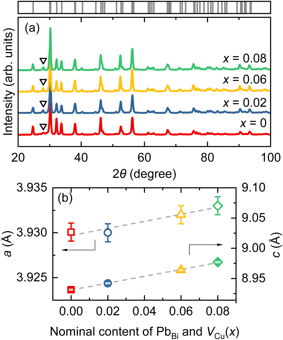 | ||
| Fig. 1 (a) Powder XRD patterns of the Bi1−xPbxCu1−xSeO (x = 0, 0.02, 0.06, and 0.08) samples. Braggs reflections for the BiCuSeO phase are indicated by gray ticks on the top part of the figure. Diffraction peak corresponding to the Bi2O3 secondary phase is indicated by a black triangle (∇). (b) Lattice parameters (a and c) as a function of nominal concentration of PbBi and VCu. | ||
In the case of dual doping, the evolution of lattice parameters can be affected by two competing factors. On the one hand, Cu deficiency tends to decrease both lattice parameters a and c,13 while on the other hand, a larger ionic radius of Pb2+ (1.19 Å) as compared to that of Bi3+ (1.03 Å)19 should result in an increase of lattice parameters.20,21 Our experimental results reveal that, even with a simultaneous increase in the concentration of PbBi and VCu, both lattice parameters a and c exhibit a gradual increase (Fig. 1b), resulting in the expansion of the unit cell volume. However, it is noteworthy that the effect of copper vacancies is noticeable, and for samples with the same nominal concentration x, the lattice parameters of dually doped specimens are slightly smaller than those of the single Pb-doped ones.20–22
Fig. 2 displays a SEM micrograph, providing an overview of the microstructure representative of all samples. Randomly arranged platelet grains are stacked densely, which is reflected in the high relative densities of all samples (≥95% of theoretical density). The thickness of the grains ranges from 300 to 600 nm. EDS analysis confirms that the actual compositions of the samples closely align with the nominal ones (Table S1, ESI†).
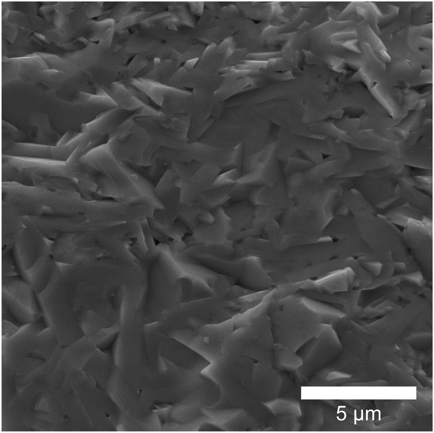 | ||
| Fig. 2 SEM micrograph of the fractured cross-section of the Bi0.94Pb0.06Cu0.94SeO sample. | ||
Fig. 3a shows the temperature dependence of electrical conductivity σ of Bi1−xPbxCu1−xSeO (x = 0, 0.02, 0.06, and 0.08) samples. For all the samples, σ gradually decreases with the increase of temperature, exhibiting a metal-like behavior as expected for heavily doped semiconductors.23 As the content of PbBi and VCu increases from 0 to 0.08, σ is vastly improved from ∼30 Ω−1 cm−1 for the pristine BiCuSeO sample to ∼450 Ω−1 cm−1 for Bi0.92Pb0.08Cu0.92SeO at room temperature. Considering only a slight improvement in the weighted mobility μw (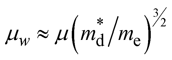 , where
  is the density of states effective mass and me is the electron mass) as shown in Fig. S1 (ESI†), the main reason for such a significant enhancement of the electrical conductivity is due to the increase in the charge carrier concentration, which is also in agreement with previous reports.22,24 Furthermore, the carrier density increase originates mostly from the substitution of Bi3+ with Pb2+, as even introducing only dual vacancies VBi and VCu in BiCuSeO led to an order of magnitude lower conductivity in comparison with the Pb-substituted ones.12 Nonetheless, as discussed in the Introduction section, the introduction of vacancies plays not a primary but a complementary role, leading to a more pronounced delocalization of charge carriers between the layers, thereby promoting interlayer charge transfer.14 This, in turn, allows for the retention of higher charge carrier mobility values at the same level of charge carrier concentration (see Fig. 12 in ref. 15).
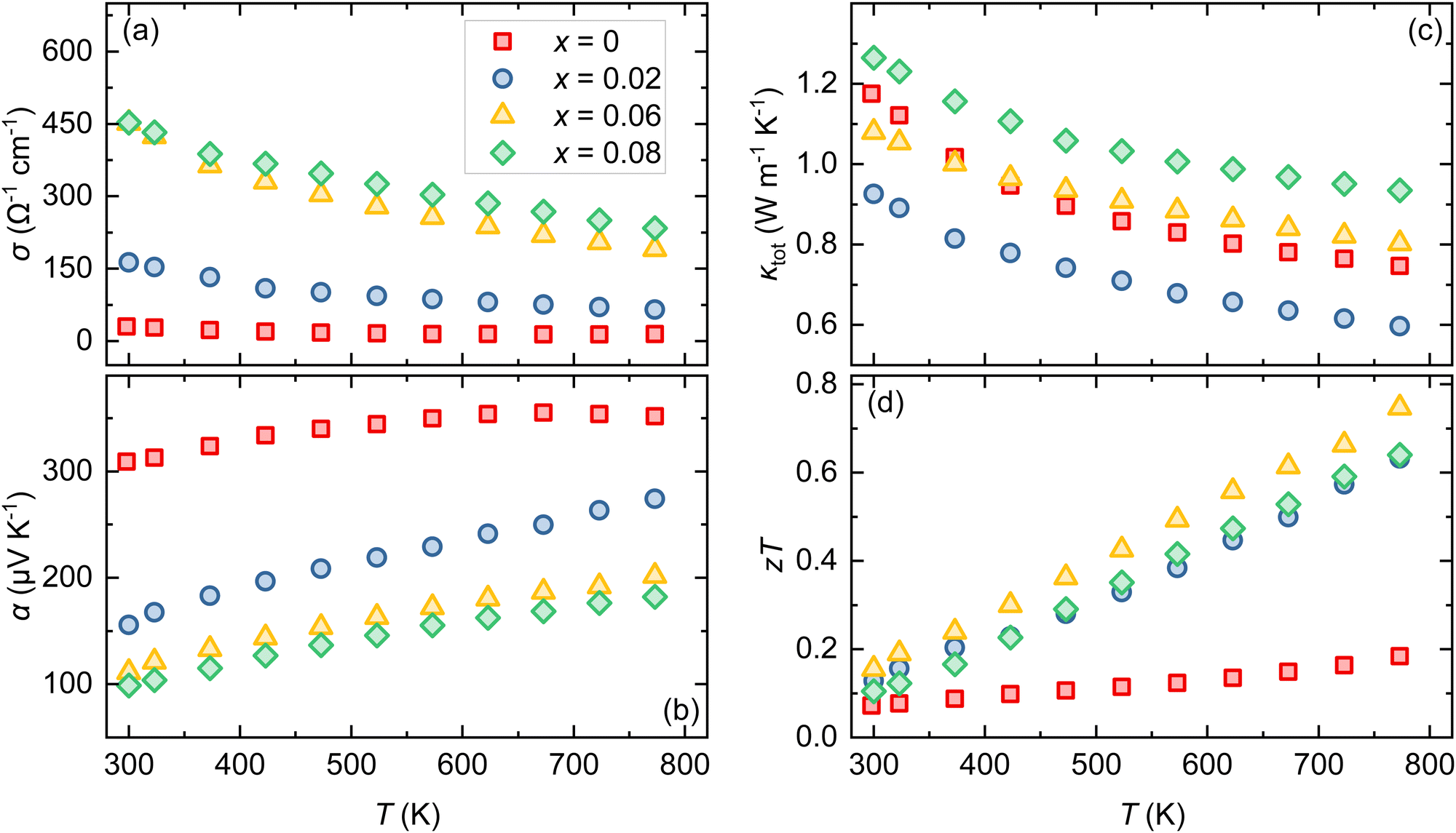 | ||
| Fig. 3 Temperature dependence of the (a) electrical conductivity σ, (b) seebeck coefficient α, (c) total thermal conductivity κtot, and (d) the figure of merit zT for Bi1−xPbxCu1−xSeO (x = 0, 0.02, 0.06, and 0.08) samples. | ||
Fig. 3b illustrates the Seebeck coefficient α as a function of temperature for Bi1−xPbxCu1−xSeO (x = 0, 0.02, 0.06, and 0.08) samples. The positive Seebeck coefficient for all samples in the entire temperature range confirms p-type conduction, indicating that holes are the majority charge carriers. The highest Seebeck coefficient throughout the investigated temperature range is observed in nominally undoped BiCuSeO. However, with the increase in PbBi and VCu concentration, α gradually decreases consistently with the changes in σ (Fig. S2, ESI†). Considering the relationship between the Seebeck coefficient and carrier concentration in semiconductors,2 such a simultaneous change in electrical conductivity and the Seebeck coefficient further underscores that it is primarily driven by a significant increase in charge carrier concentration, as was discussed previously. Consequently, at 773 K, α reduced from 352 μV K−1 for x = 0 to 182 μV K−1 for x = 0.08. The achieved optimal balance between σ and α results in a significant enhancement in the power factor (α2σ), showing more than a fourfold increase at 773 K, from 1.8 μW cm−1 K−2 to 7.7 μW cm−1 K−2, as the PbBi and VCu content is raised from x = 0 to 0.08 (Fig. 4a and Fig. S3, ESI†).
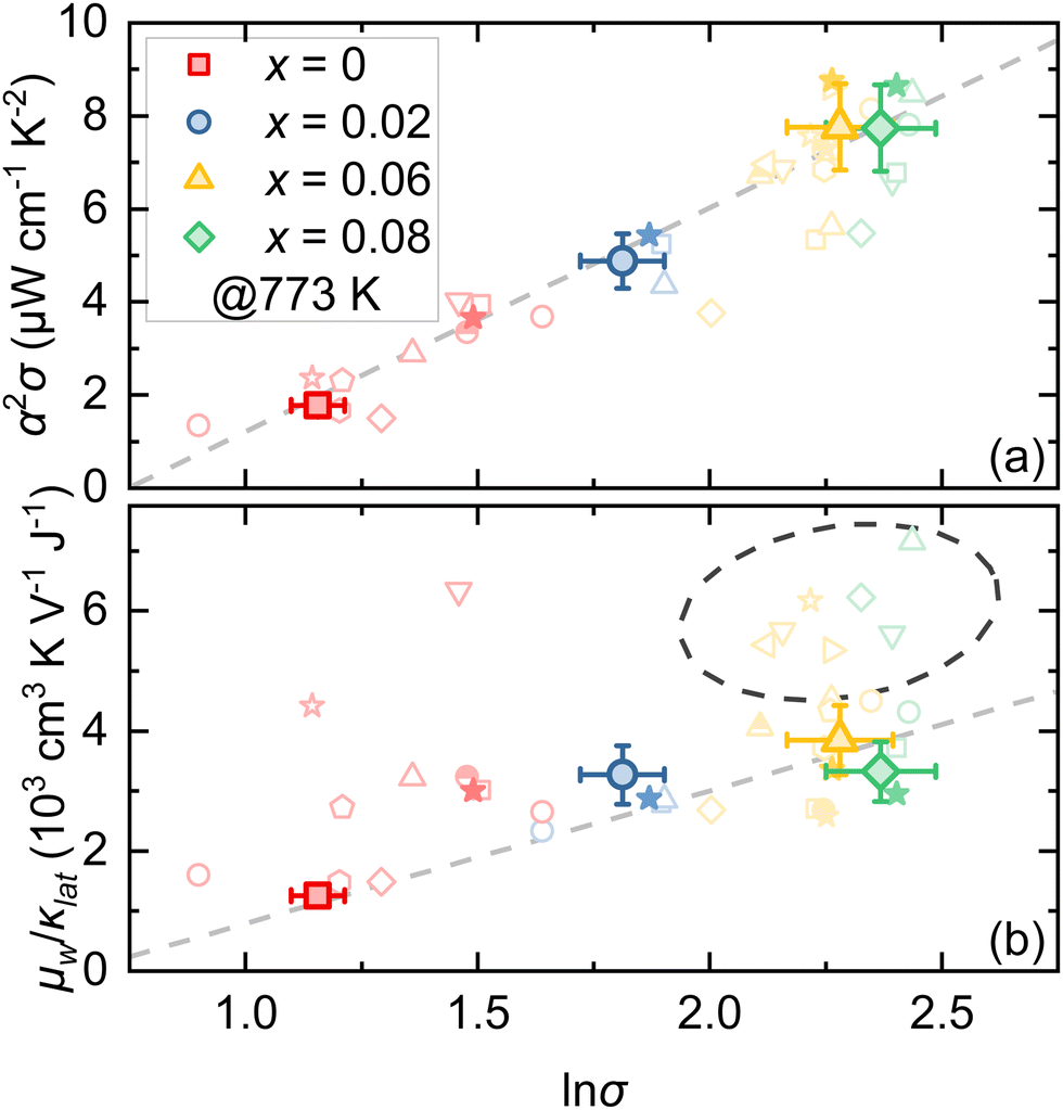 | ||
| Fig. 4 (a) Power factor α2σ and (b) μw/κlat ratio as a function of lnσ for the Bi1−xPbxCu1−xSeO (x = 0, 0.02, 0.06, and 0.08) samples. Literature data for other Bi1−xPbxCuSeO-based oxyselenides are also shown for comparison (Chen et al.,24 Gu et al.,29,32 Lan et al.,18 Lei et al.,33 Li et al.,34 Liang et al.,35 Liu et al.,36 Pan et al.,37 Ren et al.,30,31 Xu et al.,38 and Zhu et al.14). All displayed data points correspond to values obtained at 773 K. | ||
Fig. 3c shows the temperature-dependent total thermal conductivity κtot (T) of Bi1−xPbxCu1−xSeO (x = 0, 0.02, 0.06, and 0.08) samples. For pristine BiCuSeO, κtot decreases from 1.17 W m−1 K−1 at 300 K to 0.75 W m−1 K−1 at 773 K. Following simultaneous Bi to Pb substitution and Cu vacancy introduction, κtot initially decreases (x = 0.02) and then rises to 0.93 W m−1 K−1 at 773 K (x = 0.08). This can be understood by considering the evolution of both the lattice κlat and electronic κel components of total thermal conductivity. The κlat is calculated from κlat = κtot − κel, where κel can be determined through the Wiedemann–Franz law, expressed as κel = LσT, with L representing the Lorentz number.2 The Lorentz number is estimated with sufficient accuracy within the single parabolic band model with acoustic phonon scattering from experimental α values as L = 1.5 + exp{−|α|/116}.25 Owing to a significant enhancement in σ, the changes in κtot become more apparent. In pristine BiCuSeO, κel contributes to approximately 2% of the total, but this contribution rises up to over 30% with an increase in PbBi and VCu concentration (Fig. S4, ESI†). Analysis of the κlat (T) reveals that point defects are the dominant phonon scattering mechanism, evidenced by a decrease of κlat with temperature as T−0.5 for all the samples (Fig. S5, ESI†). However, for the samples with x > 0.02 κlat slightly increases but still remains lower than that of pristine BiCuSeO. This increase could be attributed to an increase in the grain size, sound velocities, and/or Pb–O bond strength due to the introduction of PbBi and VCu.26
Combining the electrical and thermal transport properties, the figure of merit zT as a function of temperature is calculated and displayed in Fig. 3d. For Bi1−xPbxCu1−xSeO samples (x > 0), the zT values are enhanced over the entire test temperature range by more than 3 times. This improvement is mainly attributed to a significant boost in the power factor, leading to a zTmax value of 0.75 at 773 K for Bi0.94Pb0.06Cu0.94SeO. On the one hand, a nearly threefold increase in zT was achieved compared to undoped BiCuSeO. On the other hand, we must admit that this is not the highest zT value achieved for Bi1−xPbxCuSeO-based oxyselenides. Furthermore, a detailed analysis of literature data reveals that reported zT values for Pb-doped BiCuSeO are scattered between 0.56 and 1.05 at T = 773 K for optimally doped compositions (Fig. S6, ESI†).
To understand what causes such a discrepancy in zT values, we analyzed the literature and our data within the concept proposed by Ioffe and later reformulated by Chasmar and Stratton:2,27 an efficient thermoelectric material should have (1) an optimal charge carrier concentration and (2) a maximized μw/κlat ratio, where μw and κlat are the weighted mobility and lattice thermal conductivity, respectively. This ratio determines the maximum zT value achievable for a given material at a given temperature.28 Thus, one can notice that the achieved power factor (α2σ) for optimally doped samples (ln![[thin space (1/6-em)]](https://www.rsc.org/images/entities/char_2009.gif) σ ≈ 2.3) was around 8 W cm−1 K−2 at 773 K and was roughly the same compared to those reported previously for other Pb-doped BiCuSeO oxyselenides (Fig. 4a). In other words, regardless of the synthesis method, the optimal level of charge carrier concentration in Bi1−xPbxCuSeO-based oxyselenides is reached around lnσ = 2.3, corresponding to the Pb doping level x between 0.06 and 0.08. However, the μw/κlat ratio, on the other hand, is strongly affected by the synthesis technique (Fig. 4b). The highest values of μw/κlat are achieved for the samples synthesized/processed by techniques such as shear exfoliation,29 high-energy ball milling,18 self-propagating high-temperature synthesis,30,31etc. In such samples, lattice thermal conductivity is suppressed by about twice compared to the glassy limit (≈0.59 W m−1 K−1) at high temperature. This originates from increased phonon scattering induced by the significantly reduced grain size29 and, what is more important, introduced crystal defects, such as nanodots,18 amorphous regions,30,31etc. Thus, the abovementioned findings highlight the importance of the microstructure (grain size and shape, defects, etc.) in the thermoelectric performance of Pb-doped BiCuSeO oxyselenides.
σ ≈ 2.3) was around 8 W cm−1 K−2 at 773 K and was roughly the same compared to those reported previously for other Pb-doped BiCuSeO oxyselenides (Fig. 4a). In other words, regardless of the synthesis method, the optimal level of charge carrier concentration in Bi1−xPbxCuSeO-based oxyselenides is reached around lnσ = 2.3, corresponding to the Pb doping level x between 0.06 and 0.08. However, the μw/κlat ratio, on the other hand, is strongly affected by the synthesis technique (Fig. 4b). The highest values of μw/κlat are achieved for the samples synthesized/processed by techniques such as shear exfoliation,29 high-energy ball milling,18 self-propagating high-temperature synthesis,30,31etc. In such samples, lattice thermal conductivity is suppressed by about twice compared to the glassy limit (≈0.59 W m−1 K−1) at high temperature. This originates from increased phonon scattering induced by the significantly reduced grain size29 and, what is more important, introduced crystal defects, such as nanodots,18 amorphous regions,30,31etc. Thus, the abovementioned findings highlight the importance of the microstructure (grain size and shape, defects, etc.) in the thermoelectric performance of Pb-doped BiCuSeO oxyselenides.
Conclusions
The thermoelectric properties of the Bi1−xPbxCu1−xSeO (x = 0, 0.02, 0.06, and 0.08) samples prepared via a solid-state reaction route followed by spark plasma sintering have been studied. The combination of Pb for Bi substitution and Cu vacancy introduction increases the electrical conductivity while moderately decreasing the Seebeck coefficient. The intrinsically low thermal conductivity of BiCuSeO is noticeably decreased by the introduction of a low concentration (x = 0.02) of PbBi and VCu and increased with a further increase in x. The optimum balance between the Seebeck coefficient and electrical conductivity was achieved for x = 0.06, while for x > 0.02, the μw/κlat ratio essentially does not increase and remains at the same level as for x = 0.02, limiting the potentially achievable zTmax. As a result, the value of zT was eventually increased by more than 3 times compared to the undoped BiCuSeO, and zTmax = 0.75 at 773 K was achieved for Bi0.94Pb0.06Cu0.94 SeO. By careful analysis of the literature data and comparing them with our results, we revealed that for Bi1−xPbxCuSeO-based oxyselenides, the main factor determining zTmax is the κlat. We believe that highlighting the mechanisms determining the zT value of doped BiCuSeO will help future researchers to develop more effective synthesis/doping strategies.Author contributions
Aleksandra Khanina: investigation, formal analysis, visualization, writing – original draft, writing – reviewing and editing; Andrei Novitskii: conceptualization, formal analysis, investigation, methodology, visualization, writing – original draft, writing – reviewing and editing; Daria Pashkova: data curation, investigation, formal analysis, visualization; Andrei Voronin: project administration, funding acquisition; Takao Mori: resources, funding acquisition, supervision, writing – reviewing and editing; and Vladimir Khovaylo: resources, supervision, writing – reviewing and editing.Conflicts of interest
There are no conflicts to declare.Acknowledgements
The study was carried out with financial support from the Russian Science Foundation, project No. 19-79-10282. T.M. and A.N. acknowledge JST Mirai JPMJMI19A1.Notes and references
- D. Sarma, Essential considerations for reporting thermoelectric properties, 2021.
- A. F. Ioffe, Semiconductor Thermoelements, and Thermoelectric Cooling, Infosearch, 1957 Search PubMed.
- R. Freer, D. Ekren, T. Ghosh, K. Biswas, P. Qiu, S. Wan, L. Chen, S. Han, C. Fu and T. Zhu, et al. , J. Phys.: Energy, 2022, 4, 022002 CAS.
- L. Kholodkovskaya, L. Akselrud, A. Kusainova, V. Dolgikh and B. Popovkin, Mater. Sci. Forum, 1993, 693–696 CAS.
- A. Kusainova, P. Berdonosov, L. Akselrud, L. Kholodkovskaya, V. Dolgikh and B. Popovkin, J. Solid State Chem., 1994, 112, 189–191 CrossRef CAS.
- L.-D. Zhao, J. He, D. Berardan, Y. Lin, J.-F. Li, C.-W. Nan and N. Dragoe, Energy Environ. Sci., 2014, 7, 2900–2924 RSC.
- Y. Liu, L.-D. Zhao, Y. Zhu, Y. Liu, F. Li, M. Yu, D.-B. Liu, W. Xu, Y.-H. Lin and C.-W. Nan, Adv. Energy Mater., 2016, 6, 1502423 CrossRef.
- Y.-L. Pei, H. Wu, D. Wu, F. Zheng and J. He, J. Am. Chem. Soc., 2014, 136, 13902–13908 CrossRef CAS PubMed.
- M. Y. Toriyama, J. Qu, G. J. Snyder and P. Gorai, J. Mater. Chem. A, 2021, 9, 20685–20694 RSC.
- D. Goury, E. Amzallag, D. Bérardan and J. Creuze, J. Phys. Chem. C, 2022, 126, 5960–5969 CrossRef CAS.
- W. Xu, Y. Liu, L.-D. Zhao, P. An, Y.-H. Lin, A. Marcelli and Z. Wu, J. Mater. Chem. A, 2013, 1, 12154–12158 RSC.
- Z. Li, C. Xiao, S. Fan, Y. Deng, W. Zhang, B. Ye and Y. Xie, J. Am. Chem. Soc., 2015, 137, 6587–6593 CrossRef CAS PubMed.
- Y. Liu, L.-D. Zhao, Y. Liu, J. Lan, W. Xu, F. Li, B.-P. Zhang, D. Berardan, N. Dragoe and Y.-H. Lin, et al. , J. Am. Chem. Soc., 2011, 133, 20112–20115 CrossRef CAS PubMed.
- H. Zhu, Z. Li, C. Zhao, X. Li, J. Yang, C. Xiao and Y. Xie, Natl. Sci. Rev., 2021, 8, nwaa085 CrossRef CAS PubMed.
- A. Novitskii, V. Khovaylo and T. Mori, Nanobiotechnol. Rep., 2021, 16, 294–307 CrossRef CAS.
- A. Novitskii, I. Serhiienko, S. Novikov, Y. Ashim, M. Zheleznyi, K. Kuskov, D. Pankratova, P. Konstantinov, A. Voronin and O. A. Tretiakov, et al. , ACS Appl. Energy Mater., 2022, 5, 7830–7841 CrossRef CAS.
- E. Shelekhov and T. Sviridova, Met. Sci. Heat Treat., 2000, 42, 309–313 CrossRef CAS.
- J.-L. Lan, Y.-C. Liu, B. Zhan, Y.-H. Lin, B. Zhang, X. Yuan, W. Zhang, W. Xu and C.-W. Nan, Adv. Mater., 2013, 25, 5086–5090 CrossRef CAS PubMed.
- R. D. Shannon, Acta Crystallogr., Sect. A: Cryst. Phys., Diffr., Theor. Gen. Crystallogr., 1976, 32, 751–767 CrossRef.
- D. Yang, X. Su, Y. Yan, T. Hu, H. Xie, J. He, C. Uher, M. G. Kanatzidis and X. Tang, Chem. Mater., 2016, 28, 4628–4640 CrossRef CAS.
- L. Pan, D. Bérardan, L. Zhao, C. Barreteau and N. Dragoe, Appl. Phys. Lett., 2013, 102, 023902 CrossRef.
- Y. Lei, H. Yang, J. Qiu, Y. Li, F. Gao, C. Yong, L. Tao, G. Song, N. Wang and S. Peng, et al. , J. Eur. Ceram. Soc., 2022, 42, 7475–7480 CrossRef CAS.
- V. I. Fistul, Heavily doped semiconductors, Plenum Press, 1969 Search PubMed.
- Y.-X. Chen, K.-D. Shi, F. Li, X. Xu, Z.-H. Ge and J. He, J. Am. Ceram. Soc., 2019, 102, 5989–5996 CrossRef CAS.
- H.-S. Kim, Z. M. Gibbs, Y. Tang, H. Wang and G. J. Snyder, APL Mater., 2015, 3, 041506 CrossRef.
- B. Feng, G. Li, Z. Pan, Y. Hou, C. Zhang, C. Jiang, J. Hu, Q. Xiang, Y. Li and Z. He, et al. , Mater. Lett., 2018, 217, 189–193 CrossRef CAS.
- R. Chasmar and R. Stratton, Int. J. Electron., 1959, 7, 52–72 CAS.
- H. Wang, A. D. LaLonde, Y. Pei and G. J. Snyder, Adv. Funct. Mater., 2013, 23, 1586–1596 CrossRef CAS.
- Y. Gu, X.-L. Shi, L. Pan, W.-D. Liu, Q. Sun, X. Tang, L.-Z. Kou, Q.-F. Liu, Y.-F. Wang and Z.-G. Chen, Adv. Funct. Mater., 2021, 31, 2101289 CrossRef CAS.
- G.-K. Ren, S. Butt, K. J. Ventura, Y.-H. Lin and C.-W. Nan, et al. , RSC Adv., 2015, 5, 69878–69885 RSC.
- G.-K. Ren, S. Wang, Z. Zhou, X. Li, J. Yang, W. Zhang, Y.-H. Lin, J. Yang and C.-W. Nan, Nat. Commun., 2019, 10, 2814 CrossRef PubMed.
- Y. Gu, W. Ai, L. Pan, X. Hu, P. Zong, C. Chen, C. Lu, Z. Xu and Y. Wang, Mater. Today Phys., 2022, 24, 100688 CrossRef CAS.
- Y. Lei, R. Zheng, H. Yang, Y. Li, C. Yong, X. Jiang, R. Liu and R. Wan, Scr. Mater., 2021, 199, 113885 CrossRef CAS.
- F. Li, Z. Zheng, Y. Chang, M. Ruan, Z. Ge, Y. Chen and P. Fan, ACS Appl. Mater. Interfaces, 2019, 11, 45737–45745 CrossRef CAS PubMed.
- X. Liang, R. Xu, M. Kong, H. Wan, W. Bai, D. Dong, Q. Li, H. Xu, Z. Li and B. Ge, et al. , Mater. Today Phys., 2023, 34, 101084 CrossRef CAS.
- Y.-C. Liu, J.-L. Lan, B. Zhan, J. Ding, Y. Liu, Y.-H. Lin, B. Zhang and C.-W. Nan, J. Am. Ceram. Soc., 2013, 96, 2710–2713 CrossRef CAS.
- L. Pan, Y. Lang, L. Zhao, D. Berardan, E. Amzallag, C. Xu, Y. Gu, C. Chen, L.-D. Zhao and X. Shen, et al. , J. Mater. Chem. A, 2018, 6, 13340–13349 RSC.
- R. Xu, Z. Chen, Q. Li, X. Yang, H. Wan, M. Kong, W. Bai, N. Zhu, R. Wang and J. Song, et al. , Research, 2023, 6, 0123 CrossRef CAS PubMed.
Footnote |
| † Electronic supplementary information (ESI) available. See DOI: https://doi.org/10.1039/d4cp00308j |
| This journal is © the Owner Societies 2024 |