Microstrain effects of laser-ablated Au nanoparticles in enhancing CZTS-based 1 Sun photodetector devices†
Received
18th January 2024
, Accepted 26th February 2024
First published on 27th February 2024
Abstract
Copper zinc tin sulfide (CZTS) thin films were synthesized on soda lime glass using pulsed laser deposition (PLD) at room temperature. Introducing gold nanoparticles (AuNPs) in a sandwich structure led to increased CZTS particle size and a shift in the localized surface plasmon resonance (LSPR) peak of the AuNPs, influenced by different laser energy levels. The absorption measurements revealed intriguing behavior across the visible and near-infrared (NIR) regions, making these films appealing for 1 Sun photodetectors. Furthermore, the presence of AuNPs in the sandwich structure reduced microstrain effects, measuring 1.94 × 10⁻³ compared to 3.38 × 10⁻³ in their absence. This reduction directly enhances carrier transport, which is particularly beneficial for accelerating the performance of photodetector devices. This effect of AuNPs also contributed to higher dielectric coefficients, further improving the photodetector performance. Under 1 Sun illumination conditions, this enhancement resulted in a rapid rising time of 95.4 ms, showcasing the potential for faster photodetection.
1. Introduction
CZTS material, which is used as an active and absorber layer in solar cells, has a distinctive feature of a high absorption coefficient (>104 cm−1) in the visible region and consists of low-cost and non-toxic elements.1–3 The high-absorbing CZTS material could be used in photodetectors and solar cell applications. Photodetectors are pivotal in diverse fields, encompassing communications, imaging, and environmental sensing. Nevertheless, prevailing challenges such as response speed, sensitivity, and fabrication cost necessitate continuous advancement in photodetector materials. In this context, CZTS thin films offer an intriguing avenue for exploration, leveraging their unique properties to address these challenges.4,5
Light trapping methods increase the absorbency of thin films produced at very low thicknesses. Among these methods, plasmonic nanoparticles (NPs) can be composed of Au, Cu, and Ag metals. These plasmonic NPs exhibit remarkable optical properties like localized surface plasmon resonance (LSPR).6,7 LSPR is a phenomenon where the electromagnetic field (EMF) of the light incident on the plasmonic NP stimulates the electrons in the particle, causing them to move simultaneously.8 The wavelength at which the LSPR peak appears varies with the particle size, shape, density, and environment. The technique used in producing the particle is essential in changing the morphological structure of plasmonic NPs. Particle growth can be achieved close to the desired density, size, and shape by quickly adjusting the parameters of the PLD9,10 experimental system, such as laser pulse number,11,12 laser energy, laser wavelength, and substrate temperature.13–15 A PLD system mainly consists of a laser system and a vacuum chamber. Thus, the morphological, optical, crystalline, and electrical properties of thin films produced by PLD can be easily adjusted.16–19
This study produced CZTS thin films in 61 nm and 112 nm thickness using the PLD technique, depending on the number of laser pulses. Au plasmonic NPs were grown on soda lime glass (SLG) depending on laser energy per pulse, and AuNPs@CZTS thin films were produced by embedding Au nanoparticles into CZTS thin films with the highest laser energy. Optical, morphological, crystalline, and electrical properties, including the photo-sensing properties of CZTS and AuNPs@CZTS thin films, were investigated in detail. In the subsequent sections, we present the growth technique employed, the discerned outcomes, an in-depth analysis, and the overarching implications of our findings. This endeavor not only furthers our understanding of photodetector materials but also underscores the potential of CZTS thin films and plasmonic NPs in shaping the future of optoelectronic devices.
2. Fabrication and characterization
A Continuum Minilite II pulsed laser device operating at 1064 nm wavelength, five ns pulse width, and 10 Hz repetition rate was used to deposit CZTS and AuNPs@CZTS thin films. The target–substrate distance in the vacuum chamber was set at 45 mm, and the atmosphere inside the vacuum chamber was evacuated down to 10−6 mbar background pressure to form a clean environment for deposition. First, the Au sputtering target (99.95%) was ablated by a laser beam with 36 mJ, 32 mJ, 30 mJ, and 26 mJ energies per pulse, and its NP thin film was deposited on the SLG substrate at room temperature.
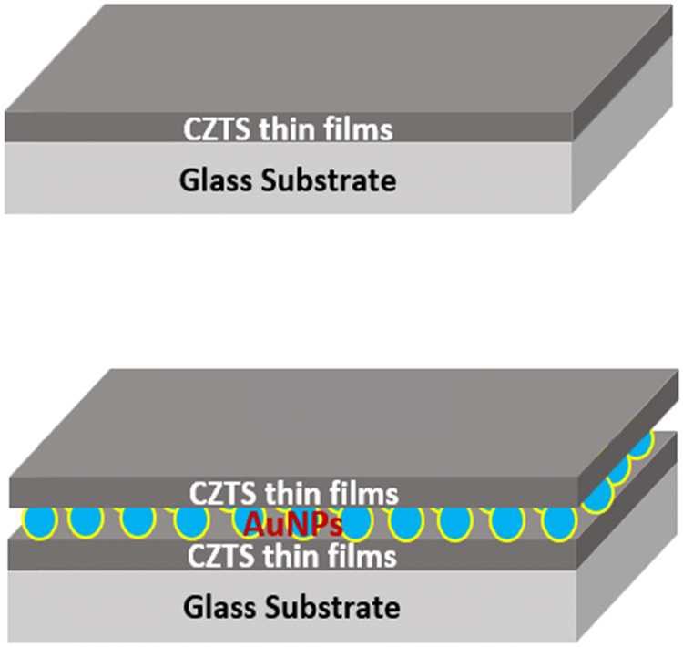
Second, the CZTS sputtering target, with a purity of 99.99%, underwent ablation by a laser beam set at a pulse energy of 15 mJ. The process utilized 2400 pulses to deposit CZTS(1) thin films with a thickness of 61 nm and 4800 pulses for CZTS(2) thin films measuring 112 nm in thickness, both on soda lime glass (SLG) substrates at ambient temperature. Au nanoparticles were ablated using 36 mJ laser pulse energies, which were embedded into these CZTS(1) and CZTS(2) thin films, and thus the plasmonic AuNPs@CZTS(1) & AuNPs@CZTS(2) thin films were produced. The sulfurization process involved subjecting the material to a quartz tube furnace under vacuum conditions, maintaining a temperature of 375 °C for 45 minutes. During this process, 50 mg of sulfur powder was placed adjacent to the material undergoing treatment. The final structure is schematically shown in Fig. 1.
 |
| | Fig. 1 Schematic design of CZTS and AuNPs@CZTS thin-film photodetectors. | |
2.1. Device characterization
The crystalline, optical, and morphological properties of CZTS and AuNPs@CZTS thin films were examined using several analytical techniques. Structural and phase parameters were analyzed using a Panalytical Empyrean instrument with CuKα radiation through X-ray diffractometry. Surface morphology was investigated using a ZEISS GeminiSEM 500 scanning electron microscope (SEM). The optical absorption spectra were measured using a 200–2000 nm UV-Vis-NIR spectrophotometer. The electrical properties of the thin film samples were assessed through electrical current–voltage (I–V) and optoelectronic measurements using an OptoSense solar simulator connected to a source meter. The light source has an AM1.5G filter at 1 Sun of 100 mW cm−2 illumination.
3. Results and discussion
3.1. XRD analyses
CZTS(1) and CZTS(2) thin films of 61 nm and 112 nm thicknesses and AuNPs@CZTS(1) & (2) thin films are produced by embedding AuNPs into these thin films. All CZTS thin films present (112), (200), and (220) crystal orientations located at 28°, 33°, and 47° (2Θ) in the XRD pattern in Fig. 2a, respectively.1 CZTS(1)-thin film indicates the weakest crystal structure. The crystal structure of CZTS(2)- thin film has been developed, and its central peak density is higher. As the number of laser pulses increased, the deposited atoms nucleated better on the substrate, filled the appropriate vacancies, and made better alignment in the crystal structure.1 In AuNPs@CZTS thin films, (111) crystal-oriented peaks of the Au element also appeared on the 2Θ = 38° angle.20 The number of Au atoms is excessive for the very thin CZTS(1) thin film, so that it can occupy undesirable places in the crystal structure. Thus, the central peak of AuNPs@CZTS(1) has been weakened. However, with the addition of AuNPs, the central peak density of the AuNPs@CZTS(2) thin film increases, and its crystal structure improves.20,21
 |
| | Fig. 2 (a) XRD spectrum of CZTS and AuNPS@CZTS thin films, (b) Raman spectrum of CZTS1 thin film. | |
Fig. 2b presents the Raman spectroscopic analysis of the CZTS1 thin film. The dominant peak at 337 cm−1 is indicative of the kesterite Cu2ZnSnS4 phase.22–24 Additionally, two secondary peaks at 267 cm−1 and 290 cm−1 are observed, corresponding to the Cu2SnS3 (CTS) secondary phase.25,26 The emergence of the CTS phase is likely due to the predominance of Sn over Zn despite a marginally reduced Cu content,27,28 as quantified in Table 2.
The primary grain size of all CZTS thin films has been calculated via the Scherrer equation that is stated by eqn (1):1
| | D = 0.94λ/β![[thin space (1/6-em)]](https://www.rsc.org/images/entities/char_2009.gif) Cosθ Cosθ | (1) |
D is the crystal size, λ is the wavelength of X-ray, θ is the Bragg diffraction angle, and β is the full-width at half-maximum of diffraction of the central peak. Crystal sizes of CZTS(1), AuNPs@CZTS(1), CZTS(2), and AuNPs@CZTS(2) thin films have been determined to be 7.34 nm, 12.1 nm, 10.71 nm, and 18.64 nm, respectively. The crystal size expanded with increases in thin film thicknesses from CZTS(1) to CZTS(2). So, with some gains in the number of laser pulses, the deposition rate increases, and thus, the grain size increases. Grain boundaries were decreased, and the traps and defects in these boundaries were passivized. Thus, the crystal structure of CZTS(2) has improved. The crystal size of AuNPs@CZTS thin films is more significant than that of non-Au embedded CZTS thin films. Au3+ ions can occupy Zn2+ vacancies. Since the Au3+ ionic radius (85 p.m.) is more comprehensive than the Zn2+ ionic radius (74 p.m.), it causes some increases in the crystal size of AuNPs@CZTS thin films.29,30 However, since the density of AuNPs in AuNPs@CZTS(1) was excessive compared to the thickness of CZTS(1) thin film, and the intensity of the prominent peak in the (112) direction that is weakened by occupying the unsuitable voids in the crystal structure.31–33 Since the thin film of CZTS(2) was thicker, the density of AuNPs did not adversely affect its crystal structure; on the contrary, the density of the main peak was enhanced.
The dislocation density (δ) and microstrain (ε) expressed by eqn (2) and (3) cause the formation of defect structures in the thin films and the deterioration of their crystal structure.
| |  | (2) |
| |  | (3) |
As presented in Table 1, since CZTS(1) has a smaller grain size, there are many defects and traps within the grain boundary numbers, and δ and ε are high. The grain size of AuNP@CZTS(2) is wider than the other thin films, δ and ε reduced because the grain boundary numbers are decreased. Furthermore, since plasmonic NPs enhance grain size, the dislocation density and microstrain of CZTS thin films are diminished.16 The measurement of microstrain, which accounts for these lattice effects, signifies a decrease from 3.38 × 10⁻³ to 1.94 × 10⁻³ due to the presence of AuNPs. This decrease indicates that the lattice distortions within the material are less pronounced or mitigated when AuNPs are incorporated into the structure.
Table 1 Grain size, dislocation density, microstrain, and crystalline number of CZTS and AuNPS@CZTS thin films
| Samples |
Grain size (nm) |
Dislocation density × 1016 (lines per m2) |
Micro-strain × 10−3 |
| CZTS(1) |
7.34 |
1.86 |
4.93 |
| AuNPs@CZTS(1) |
12.1 |
0.68 |
2.99 |
| CZTS(2) |
10.71 |
0.72 |
3.38 |
| AuNPs@CZTS(2) |
18.64 |
0.28 |
1.94 |
3.2. SEM analysis
SEM images of Au NP thin films deposited by 26 mJ and 36 mJ laser pulse energies are given in Fig. 3a and b. While the particles grown on the substrate with low laser pulse energies were small and low in density, the particles produced with large size and high density were realized by high laser pulse energies. So, since fewer Au atoms are ablated with low laser energies, the plasma volume formed by these atoms is tiny, as seen in the inset of Fig. 3a. In addition, the kinetic energy of the ablated atoms is low. Therefore, since the density and points of atoms coming on the substrate are low, the nucleation and particles formed by these atoms are small in size, and the particle density is low. However, it is found to be more significant in the higher energetic and dense plasma of Au atoms formed by higher-laser pulse energies, shown as an inset of Fig. 3b. The highly energetic Au particles attributed to the AuNPs clusters are in Fig. 3b.34
 |
| | Fig. 3 SEM image of Au nanoparticles (and the plasma photograph of the ablated Au material) of the deposited Au nanoparticles by (a) 26 mJ and (b) 36 mJ laser energy. | |
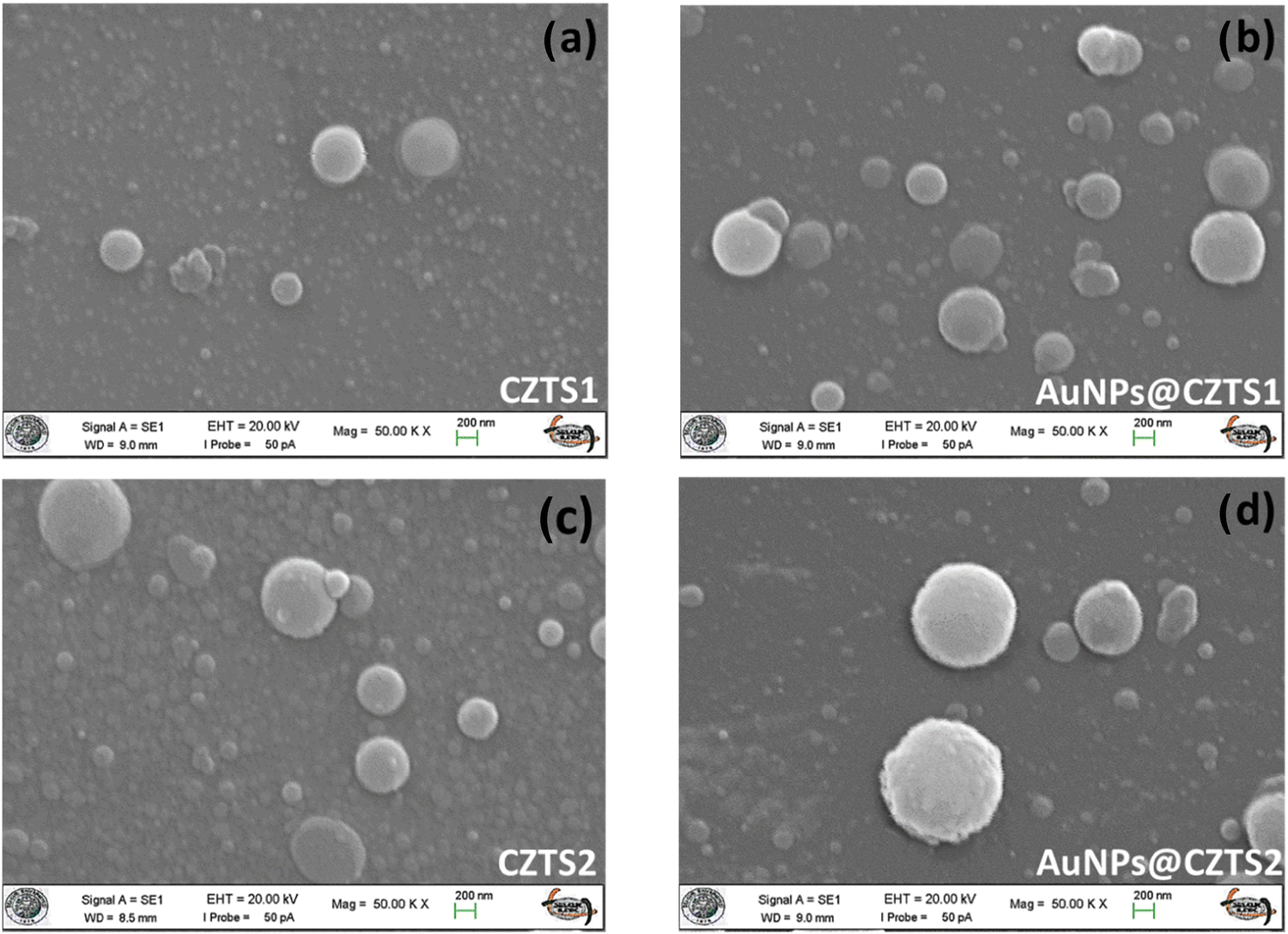
CZTS(1) thin films are formed from particles of 250 nm size in Fig. 4a. As the deposition rate increases, particle aggregation and growth improve, the particles constructing CZTS(2) thin film are more significant.35 CZTS(2) constituted from about 400 nm sized particles, as shown in Fig. 4c. AuNPs ablated by 36 mJ laser pulse energy were embedded into CZTS(1) and CZTS(2) thin films. Embedding AuNPs into CZTS thin films causes the particle agglomeration to grow and the particle size to increase, as stated above. Therefore, the size of particles making up AuNPs@CZTS thin films is comparable to the non-embedded CZTS thin films. In Fig. 4b and d, it can be seen that the particle size of AuNPs@CZTS(1) & (2) thin films increased pronouncedly.1,36,37
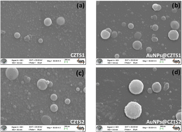 |
| | Fig. 4 SEM images of CZTS and AuNPS@CZTS thin films. | |
3.3. SEM-EDX analyses
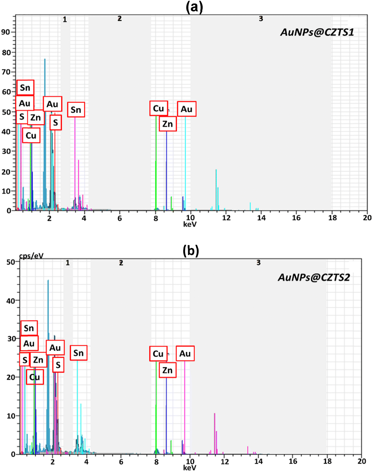
Fig. 5 and Table 2 show that AuNPs@CZTS thin films are rich in Sn because the 375 °C annealing temperature is not very high. However, during the annealing process of thin films, Sn elements tend to evaporate and diffuse towards the film surface, which causes the amount of Sn in a thin film to be excessive on the surface.38–41 The amount of Cu is higher than that of Zn, indicating that Zn2+ ions have replaced Au3+ ions. Increasing the thickness of thin films led to some decrease in Sn and a more ideal stoichiometric transfer. CuZn acceptor defects can occur in AuNPs@CZTS(2), a thin film that enhances its p-type feature.42 Furthermore, the Zn/Sn ratio increase indicates that AuNPs@CZTS(2) thin film turns into an ideal stoichiometric structure.
 |
| | Fig. 5 SEM-EDX spectra of (a) AuNPs@CZTS(1) and (b) AuNPs@CZTS(2) thin films. | |
Table 2 Atomic weights of elements constituting AuNPs@CZTS(1) and AuNPs@CZTS(2) thin films
| Thin films |
Cu (%) |
Au (%) |
Zn (%) |
Sn (%) |
S (%) |
| AuNPs@CZTS(1) |
24.03 |
6.66 |
8.78 |
27.34 |
33.18 |
| AuNPs@CZTS(2) |
27.33 |
6.32 |
8.32 |
20.14 |
37.89 |
3.4. Optical analyses
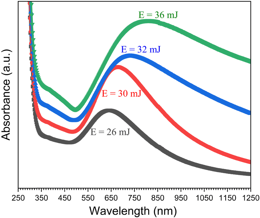
The absorption spectrum of AuNPs ablated by the laser beam with energies in the 26 mJ and 36 mJ range and then deposited on substrates is given in Fig. 6. The deposited AuNPs have exhibited LSPR properties. The LSPR peak shifted towards the more extended wavelength region in the solar spectrum while the laser beam energy increased. So, the density of ablated particles deposited on the substrate shows some increment with some increase in laser energies. The near-field interaction between AuNPs and larger particle sizes causes the redshift. LSPR peaks of particles deposited using 36 mJ, 32 mJ, 30 mJ, and 26 mJ laser energies appeared at 820 nm, 725 nm, 686 nm, and 648 nm positions in the spectrum, respectively.43 The particles deposited using 26 mJ laser pulse energy have a low density and a small particle size. Electrons in the particle are excited by the EMF of the radiation, making simultaneous oscillating motion and providing the damping of the electric field of the light by the dipole field.44–46 The large particle size and the near-field interaction between the particles can result in some distortion of the oscillation by affecting the restoring force that causes the movement of electrons in the particle, leading to the LSPR peak shifting towards the more extended wavelength region.
 |
| | Fig. 6 The absorption spectra of Au plasmonic nanoparticles depending on laser pulse energy. | |
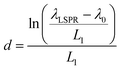
Depending on the LSPR peak wavelength, the size of NP forming the Au thin film can be calculated by eqn (4):
| |  | (4) |
where
λ0 = 530 nm is the primary LSPR wavelength for Au nanoparticles;
L1 = 6.53 and
L2 = 0.0212, are constants and
λLSPR is the LSPR wavelength of thin films produced.
47 NPs forming Au thin films were calculated to be 175 nm, 157 nm, 146 nm, and 133 nm for LSPR peaks that appeared at 820 nm, 725 nm, 686 nm, and 648 nm wavelengths, respectively. As stated above, some increases in the LSPR peak confirmed the increase in the particle size.
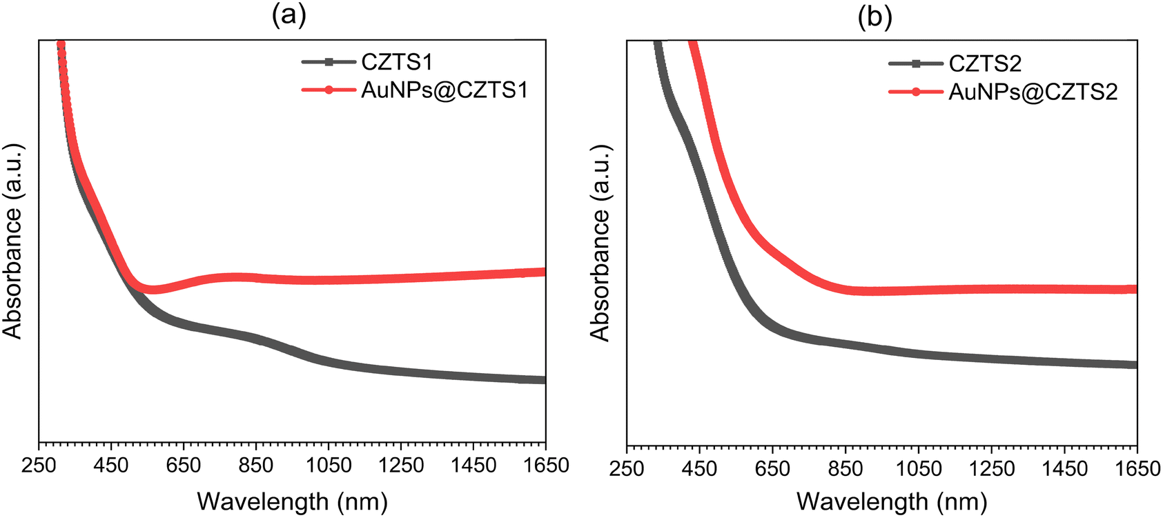
In the absorption spectrum presented in Fig. 7a, it is observed that the CZTS(1) thin film without embedded AuNPs exhibits a lower absorption intensity in the near-infrared (NIR) and visible (Vis) regions compared to the AuNPs@CZTS(1) sample. AuNPs@CZTS(1) demonstrates an enhanced absorption capacity, notably presenting a localized surface plasmon resonance (LSPR) peak at a wavelength of 763 nm, attributable to the plasmonic properties of the embedded gold nanoparticles (AuNPs). This enhancement in absorption intensity in the Vis and NIR regions is a direct consequence of the presence of AuNPs. Furthermore, the AuNPs@CZTS(2) thin film, doped with AuNPs using a 36 mJ laser pulse energy, exhibits even higher absorption intensity in these regions than the CZTS(1) thin film. This difference highlights the significant role of laser energy in modulating the optical properties of the AuNP-doped CZTS films.
 |
| | Fig. 7 The absorption spectra of (a) CZTS(1) & (2) and (b) AuNPs@CZTS(1) & (2) thin films. | |
The Tauc equation expressed below is used to calculate the band gap of thin films:
E
g is the thin film band gap, A is a constant, and hv is the photon energy. The extrapolation of the linear line of (αhv)2versus (hv) in the Tauc plot allows Eg to be obtained as in Fig. 8. The direct band gaps of CZTS(1), CZTS(2), AuNPS@CZTS(1), and AuNPS@CZTS(2) thin films have been determined to be 1.95 eV, 1.90 eV, 1.85 eV, and 1.52 eV, respectively. It has been noticed that the absorption of thin films increases with the doping of AuNPs while their band gap decreases.48 In addition, Au atoms can lead to some decreases in the band gap as they can form shallow defects in the band gap. Therefore, more photo-excited charge carriers can be included inside thin films with a lower band gap.
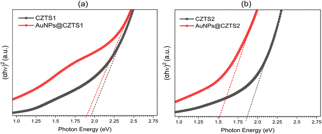 |
| | Fig. 8 The Tauc plot of (a) CZTS(1) & (2) and (b) AuNPs@CZTS(1) & (2) thin films. | |
The refractive index of CZTS and AuNPS@CZTS semiconductors is a parameter that significantly affects the optical properties of thin films. Different models for calculating the refractive index were reported in this section. The Moss relation, expressed by eqn (6), was used to calculate the refractive index of a thin film:49
where,
k is a constant = 108 eV. In addition, the Herve–Vandamme
50 relation indicates the relation between
Eg and
n.
| |  | (7) |
here,
X and
Y are constants with values of 13.6 eV and 3.4 eV, respectively. Furthermore, Ravindra also interestingly revealed the relationship between
n and
Eg, using
eqn (8).
16
Moss’ and Herve–Vandamme's relations indicate very compatible results with each other. However, although Ravindra's relations are consistent, their values are somewhat small compared to those obtained from the other relations. This can be attributed to the coefficient and multiplier values used in the equations. Nevertheless, the increase in the photon absorption and decrease in the band gap with the embedding of AuNPs caused an increase in the refractive index of CZTS thin films. Therefore, CZTS(1), exhibiting the highest photon transmission, has a low refractive index, while AuNPs@CZTS(2), a thin film with the highest photon absorbance, indicates a high refractive index.
The electric field between the charge carriers in the semiconductor represents the dielectric constant and determines the mobility and density of the charges. Therefore, the dielectric coefficient acting on the photoexcited charge carriers in the photodetector is a factor in determining the performance of the photodetectors. The static dielectric constant (εo) and the high-frequency dielectric constant (ε∞) are expressed by eqn (9) and (10):16
As seen in Table 3, AuNPs enhance the dielectric coefficients of CZTS thin films. The high dielectric coefficient facilitates the transfer of charges and mobility in the thin films, increases the lifetime of thin films, and therefore provides better responsiveness and high performance of the photodetectors. The dielectric coefficient of the weakest crystalline CZTS(1) thin film is the lowest, while that of the most advanced crystalline AuNPS@CZTS(2) thin film is the highest. Therefore, the recommendation to consider the values from Moss, Herve–Vandamme models more seriously stems from their closer alignment and higher consistency with each other, potentially indicating a more reliable prediction or closer approximation to the actual physical properties being measured. However, assessing the models in the context of specific experimental conditions or theoretical frameworks is essential to ensure the most accurate interpretation.
Table 3 Refractive index (n), high-frequency dielectric constant (ε∞) and static dielectric constant (εo) of CZTS and AuNPs@CZTS thin films
| Samples |
E
g (eV) |
Moss |
Herve–Vandamme |
Ravindra |
ε
o
|
|
n
|
ε
∞
|
n
|
ε
∞
|
n
|
ε
∞
|
| CZTS(1) |
1.95 |
2.72 |
7.44 |
2.73 |
7.46 |
2.50 |
6.26 |
12.51 |
| AuNPs@CZTS(1) |
1.90 |
2.74 |
7.53 |
2.75 |
7.58 |
2.54 |
6.47 |
12.66 |
| CZTS(2) |
1.85 |
2.76 |
7.64 |
2.77 |
7.71 |
2.58 |
6.69 |
12.82 |
| AuNPs@CZTS(2) |
1.52 |
2.90 |
8.42 |
2.93 |
8.64 |
2.86 |
8.22 |
13.83 |
3.5. Photodetector characterization
The photodetection capabilities of nanostructured CZTS and AuNPs@CZTS films were studied by analyzing their dark and 1 Sun illumination current–voltage (I–V) characteristics. The I–V behavior of CZTS and AuNPs@CZTS thin film-based photodetectors was recorded under dark and illuminated conditions over a voltage range from −5 to +5 volts, as shown in Fig. 9(a–d). Notably, all the films demonstrated impressive light detection capabilities under 1 Sun illumination.
 |
| | Fig. 9
I–V behavior (a) CZTS(1), (b) CZTS(2), (c) AuNPs@CZTS(1) and (d) AuNPs@CZTS(2) thin films. | |
In the dark current measurements, the recorded currents (Id) at a bias voltage of 5 V were found to be approximately 2.24 mA, 2.52 mA, 2.65 mA, and 3.33 mA for CZTS(1), CZTS(2), AuNPs@CZTS(1), and AuNPs@CZTS(2) films, respectively (see Fig. A1, ESI†). These values provide insights into the conductivity of thin films without illumination. The variation in dark currents can be attributed to the thickness of nanostructures and the integration of AuNPs in the CZTS matrix. Notably, the AuNPs@CZTS(2) film demonstrated the highest dark current among all the samples, suggesting its potential for enhanced charge carrier transport and sensitivity, essential for efficient photodetection applications.
This study aims to investigate the time-dependent photoresponse of photodetector CZTS devices. These devices were subjected to intense 1 Sun light pulses with an irradiance of 100 mW cm−2 to analyze their temporal behavior (Fig. 10a). The measurements were carefully conducted at a fixed bias voltage of 5.0 V. The resulting data are presented in Fig. 10b. Among the CZTS structures integrated with AuNPs, AuNPs@CZTS(2) film emerged as the most efficient device. The one-cycle time-dependent photoresponse of AuNPs@CZTS(2) film is illustrated in Fig. 10c.
 |
| | Fig. 10 Photo-switching characteristics of CZTS-based devices. (a) Schematic illustration of the measurement configuration for photoresponse speed measurement. (b) Time-resolved photoresponse at the bias voltage of 5 V under 1 Sun light illumination. (c) A magnified plot of one response cycle of AuNPs@CZTS(2) in (b) was used to obtain the response and recovery times. CZTS-based devices (d) rise and decay times (e) responsivity, detectivity, EQE, and photocurrent gain. | |
The rise and decay times of CZTS and AuNPs@CZTS PDs of 61 and 112 nm CZTS layers in thickness at 5 V are illustrated in Fig. 10d. τR rise (response) time holds significant importance in photodetectors as it signifies the duration required for the device to detect variations in light intensity and generate an output signal. τR is particularly critical in applications that demand swift detection and response, such as optical communication systems and high-speed imaging. A shorter τR enables the photodetector to respond rapidly to changes in light intensity, facilitating faster and more accurate measurements. Conversely, the decay τR (recovery) time denotes the period required for the photodetector to return to its original state after exposure to a light signal. Phononic scattering pertains to the interaction between charge carriers and lattice vibrations and can affect carrier mobility and, hence, the photodetector speed. If the CZTS2 structure, due to its increased thickness or differences in grain size, presents altered phonon scattering dynamics, this could lead to a more favorable environment for carrier transport. Conversely, increased phononic scattering in CZTS2 could be responsible for its slower response. In addition, the incorporation of AuNPs has a substantial effect on reducing, τR and τD, especially in the case of the thicker CZTS film (CZTS(2)). Consequently, the AuNPs@CZTS(2) sample exhibits faster rise (τR = 95.4 ms) and decay (τD = 98 ms) times, aligning with the expected outcomes. The plasmons in AuNPs are excited and form dipoles and the dipoles create an electric field around AuNPs. This way, photoexcited electron and hole pairs occur where the electric field enhancement between AuNPs is close. In particular, photoexcited electrons increase the number and lifetime of minority charge carriers and improve the performance of the photodetector.16,43,51,52 The LSPR effect is more pronounced in the thicker CZTS2 layer, where the presence of AuNPs effectively mitigates the negative impact of increased layer thickness on the carrier transport.
The photodetector parameters such as responsivity (R), detectivity (D*), external quantum efficiency (EQE), and photocurrent gain (G) play a crucial role in understanding the influence of the CZTS layer thickness and the incorporation of AuNPs into the CZTS layer. These parameters were calculated using the following expressions eqn (11–14):
| |  | (11) |
| |  | (12) |
| |  | (13) |
| |  | (14) |
In these equations, P represents the power of the light source, S denotes the active area of the device, and e represents the electronic charge. The results of these parameters were obtained under a bias voltage of 5.0 V and are presented in Fig. 10e.
The investigated parameters exhibited an increasing trend as the CZTS layer thickness increased. The impact of AuNPs on these parameters was found to increase the performance of the device. Consequently, the AuNPs@CZTS(2) configuration demonstrated the highest values across all the studied parameters, including a responsivity of 0.024 A W−1, a detectivity of 6.7 × 10⁸ Jones, an EQE of 0.35% and a photocurrent gain of 2.8. The performance parameters presented in Fig. 10e – which include responsivity, detectivity, external quantum efficiency (EQE), and photocurrent gain – all show an improvement as the bandgap narrows (see Fig. A2, ESI†). CZTS2, with a lower bandgap than CZTS1, exhibits a better performance, demonstrating the direct impact of bandgap engineering on the device efficacy. The reduction in the bandgap allows for more efficient absorption of the 1 Sun solar spectrum, thus increasing the generation of charge carriers under illumination. This is particularly relevant for photodetectors, where a smaller bandgap can significantly improve the absorption of low-energy photons, which constitute a substantial portion of the solar spectrum.
Previous studies have highlighted the importance of developing cost-effective and uniformly deposited CZTS thin films to enhance the performance of photodetector devices. A comprehensive examination of the existing literature on photodetector devices based on CZTS materials is presented in Table 4. However, this study proposes a novel approach to address these challenges using a simple PLD system.19 This method enables the fabrication of CZTS thin films with an incorporated plasmonic layer of AuNPs. Consequently, this approach holds significant potential for enhancing the overall performance of PD devices.
Table 4 Comparison of device performance: current device vs. previous studies on CZTS thin film-based photodetectors
| Device |
Spectral range (nm) |
R (A W−1) |
D* (Jones) |
τ
R
(ms) |
τ
D
(ms) |
Ref. |
| AuNPs@CZTS thin film |
1 Sun |
0.024 |
6.70 × 10⁸ |
95.4 |
98 |
This work |
| Na-doped CZTS thin film |
1064 |
63 |
— |
1.06 |
29.8 |
53
|
| CZTS-Au nanocomposite |
450–460 |
— |
— |
22400 |
391800 |
54
|
| CZTSSe thin film |
532 |
0.0146 |
3.5 × 10⁹ |
330 |
0.986 |
55
|
| CZTS thin film |
1000–1100 |
13 |
— |
130 |
700 |
56
|
| CZTS rice-like |
1064 |
— |
4.48 × 10⁸ |
208 |
175 |
57
|
| Au/CZTS/FTO |
750 |
0.5 |
1016 |
— |
— |
58
|
| CZTS thin film |
480 |
2.02 |
15.1 × 10⁸ |
3700 |
4100 |
59
|
Conclusions
Thin films, CZTS(1) and CZTS(2), with thicknesses of 61 nm and 112 nm, were deposited on soda lime glass utilizing a PLD system, accompanied by the incorporation of Au plasmonic nanoparticles (NPs). This integration notably augmented the grain size within the thin films while enhancing the crystal structure of CZTS(2) films. Notably, the wavelength of the localized surface plasmon resonance peak of AuNPs exhibited a shift from 648 nm to 820 nm in response to increased laser energy. The introduction of LSPR, coupled with the presence of AuNPs, significantly enhanced the NIR photon absorption capabilities of both CZTS(1) and CZTS(2) thin films. This effect resulted in a reduction of their band gaps. The calculated refractive indices, employing Moss, Herve–Vandamme, and Ravindra models, exhibited coherent values. The thin films displayed heightened diffraction indices and dielectric coefficients as the band gaps decreased. Among the fabricated photodetectors, those incorporating 112 nm-thick thin films with AuNPs (AuNPs@CZTS(2)) demonstrated superior performance, displaying the rise and decay times of τR = 95.4 ms and τD = 98 ms, respectively.
Conflicts of interest
The authors have no relevant financial or non-financial interests to disclose.
Acknowledgements
The authors are thankful to the Selcuk University's Scientific Research Projects (BAP) Coordination Office for their invaluable support, specifically through the projects numbered 15201070, 19401140, 21406007, and 22401108. Also, thanks to the Selçuk University's High Technology Research and Application Center (İL-TEK) and SULTAN Center for their crucial infrastructural support. The authors also acknowledge Necmettin Erbakan University's Science and Technology Research and Application Center (BITAM) for their contributions.
References
- S. Y. Gezgin, A. Houimi and H. Ş. Kılıç, Production and photovoltaic characterisation of n-Si/p-CZTS heterojunction solar cells based on a CZTS ultrathin active layers, Optik, 2019, 199, 163370 CrossRef CAS.
- S. Y. Gezgin and H. Ş. Kılıç, The electrical characteristics of ITO/CZTS/ZnO/Al and ITO/ZnO/CZTS/Al heterojunction diodes, Optik, 2019, 182, 356–371 CrossRef.
- S. Yiğit Gezgin and H. Ş. Kiliç, Determination of electrical parameters of ITO/CZTS/CdS/Ag and ITO/CdS/CZTS/Ag heterojunction diodes in dark and illumination conditions, Opt. Quantum Electron., 2019, 51, 1–22 CrossRef.
- S. Dursun,
et al., Investigation of photocatalytic activity (under visible light) of ultrathin CZTS films produced in different thicknesses by PLD method, Opt. Quantum Electron., 2023, 55(2), 166 CrossRef CAS.
- A. K. Singh,
et al., Impact on structural and optical properties of CZTS thin films with solvents and Ge Incorporation, Int. J. Photoenergy, 2021, 2021, 1–9 Search PubMed.
- M. A. García, Surface plasmons in metallic nanoparticles: fundamentals and applications, J. Phys. D: Appl. Phys., 2011, 44(28), 283001 CrossRef.
- S. Y. Gezgin,
et al., Effect of Ar gas pressure on LSPR property of Au nanoparticles: Comparison of experimental and theoretical studies, Nanomaterials, 2020, 10(6), 1071 CrossRef CAS PubMed.
- C. Noguez, Surface plasmons on metal nanoparticles: the influence of shape and physical environment, J. Phys. Chem. C, 2007, 111(10), 3806–3819 CrossRef CAS.
- A. Houimi, S. Y. Gezgin and H. Ş. Kılıç, The effect of sodium (Na) doping on the performance of n-Si/Cu2SnS3 heterojunction solar cells deposited by PLD using a homemade target, Optik, 2022, 264, 169364 CrossRef CAS.
- J. Polte, Fundamental growth principles of colloidal metal nanoparticles – a new perspective, CrystEngComm, 2015, 17(36), 6809–6830 RSC.
- S. Y. Gezgin, Modelling and investigation of the electrical properties of CIGS/n-Si heterojunction solar cells, Opt. Mater., 2022, 131, 112738 CrossRef.
-
H.-U. Krebs, et al., Pulsed Laser Deposition (PLD) – A Versatile Thin Film Technique, in Advances in Solid State Physics, ed. B. Kramer, Springer Berlin Heidelberg: Berlin, Heidelberg, 2003, pp. 505–518 Search PubMed.
- A. J. Haider,
et al., A comprehensive review on pulsed laser deposition technique to effective nanostructure production: trends and challenges, Opt. Quantum Electron., 2022, 54, 8 CrossRef.
- N. A. Shepelin,
et al., A practical guide to pulsed laser deposition, Chem. Soc. Rev., 2023, 52(7), 2294–2321 RSC.
- A. A. Akande, B. N. Masina and B. Mwakikunga, Effect of laser wavelength in PLD in the orientation and thermochromic properties of VO2(M1) on a glass substrate, MRS Adv., 2020, 5(21–22), 1121–1132 Search PubMed.
- S. Yiğit Gezgin and H. Ş. Kiliç, The effect of Ag plasmonic nanoparticles on the efficiency of CZTS solar cell: an experimental investigation and numerical modelling, Indian J. Phys., 2023, 97(3), 779–796 CrossRef.
- Ü. Akın,
et al., The electrical properties of ZnO/Si heterojunction diode depending on thin film thickness, J. Korean Phys. Soc., 2022, 81(2), 139–149 CrossRef.
- S. Y. Gezgin,
et al., Determination of photovoltaic parameters of CIGS hetero junction solar cells produced by PLD technique, using SCAPS simulation program, Vacuum, 2021, 192, 110451 CrossRef CAS.
- M. A. Basyooni,
et al., Observation of negative photoresponse in Joule-heated Au/Cu2SnS3 ternary chalcogenide thin film deposited by low energy pulsed laser deposition, Opt. Mater., 2022, 128, 112389 CrossRef CAS.
- A. Katerski,
et al., Modification of light absorption in thin CuInS2 films by sprayed Au nanoparticles, Nanoscale Res. Lett., 2014, 9, 1–6 CrossRef CAS.
- B. K. Patra,
et al., Coincident site epitaxy at the junction of Au–Cu2ZnSnS4 heteronanostructures, Chem. Mater., 2015, 27(3), 650–657 CrossRef CAS.
- S.-N. Park,
et al., Solution-processed Cu2ZnSnS4 absorbers prepared by appropriate inclusion and removal of thiourea for thin film solar cells, RSC Adv., 2014, 4(18), 9118–9125 RSC.
- S. Singh,
et al., Superior heterojunction properties of solution processed copper-zinc-tin-sulphide quantum dots on Si, Nanotechnology, 2017, 28(43), 435704 CrossRef PubMed.
- J. P. Liu,
et al., Fabrication and characterization of kesterite Cu2ZnSnS4thin films deposited by electrostatic spray assisted vapour deposition method, Phys. Status Solidi A, 2015, 212(1), 135–139 CrossRef CAS.
-
S. R. Kodigala, Thin film solar cells from earth abundant materials: growth and characterization of Cu2(ZnSn)(SSe)4 thin films and their solar cells, Newnes, 2013 Search PubMed.
- M. Y. Yeh,
et al., Copper-Zinc-Tin-Sulfur Thin Film Using Spin-Coating Technology, Materials, 2016, 9(7), 526 CrossRef PubMed.
- W. Bao and M. Ichimura, Influence of secondary phases in kesterite-Cu2ZnSnS4 absorber material based on the first principles calculation, Int. J. Photoenergy, 2015, 2015, 592079 CrossRef.
- D. M. Berg,
et al., Discrimination and detection limits of secondary phases in Cu2ZnSnS4 using X-ray diffraction and Raman spectroscopy, Thin Solid Films, 2014, 569, 113–123 CrossRef CAS.
- H. Hussein and A. Yazdani, Doping the bismuth into the host's Cu2ZnSnS4 semiconductor as a novel material for thin film solar cell, Results Phys., 2019, 12, 1586–1595 CrossRef.
- H. Hussein and A. Yazdani, Investigation the influence of Fe (III) doping in Cu2ZnSnS4 semiconductor: Structural, optical and magnetic properties, Optik, 2019, 179, 505–513 CrossRef CAS.
- D. S. Dhawale, A. Ali and A. C. Lokhande, Impact of various dopant elements on the properties of kesterite compounds for solar cell applications: a status review, Sustainable Energy Fuels, 2019, 3(6), 1365–1383 RSC.
- N. Khoshsirat,
et al., Efficiency enhancement of Cu2ZnSnS4 thin film solar cells by chromium doping, Sol. Energy Mater. Sol. Cells, 2019, 201, 110057 CrossRef CAS.
- D.-H. Kuo and M. Tsega, Characterizations of Ga-Doped Cu1.75Zn (Sn1−xGax)Se4 Bulks, ECS J. Solid State Sci. Technol., 2014, 3(5), P155 CrossRef CAS.
- P. K. Diwakar,
et al., The influence of laser pulse duration and energy on ICP-MS signal intensity, elemental fractionation, and particle size distribution in NIR fs-LA-ICP-MS, J. Anal. At. Spectrom., 2013, 28(9), 1420–1429 RSC.
- Z. Vakulov,
et al., Size effects in LiNbO3 thin films fabricated by pulsed laser deposition, J. Phys.: Conf. Ser., 2018, 1124, 022032 CrossRef.
- K. Rawat and P. Shishodia, Enhancement of photosensitivity in bismuth doped Cu2ZnSnS4 thin films, Phys. Status Solidi RRL, 2016, 10(12), 890–894 CrossRef CAS.
- S. Thiruvenkadam,
et al., Effect of Zn/Sn molar ratio on the microstructural and optical properties of Cu2Zn1-xSnxS4 thin films prepared by spray pyrolysis technique, Phys. B, 2018, 533, 22–27 CrossRef CAS.
- W. Feng,
et al., Influence of annealing temperature on CZTS thin film surface properties, J. Electron. Mater., 2017, 46, 288–295 CrossRef CAS.
- G. K. Gupta, V. Reddy and A. Dixit, Impact of excess and disordered Sn sites on Cu2ZnSnS4 absorber material and device performance: a 119Sn Mössbauer study, Mater. Chem. Phys., 2019, 225, 410–416 CrossRef CAS.
- L. Yao,
et al., Reactive mechanism of Cu2ZnSnSe4 thin films prepared by reactive annealing of the cu/Zn metal layer in a SnSex+ se atmosphere, Crystals, 2018, 9(1), 10 CrossRef.
- J. Zhong,
et al., Sulfurization induced surface constitution and its correlation to the performance of solution-processed Cu2ZnSn(S, Se)4 solar cells, Sci. Rep., 2014, 4(1), 1–9 Search PubMed.
-
C. Bosson, Understanding Cu2ZnSnS4 as a Photovoltaic Absorber for the Future of Solar Electricity, Durham University. 2018 Search PubMed.
- S. Y. ğt Gezg
![[i with combining dot above]](https://www.rsc.org/images/entities/char_0069_0307.gif) n and H. Ş. Kılıç, An improvement on the conversion efficiency of Si/CZTS solar cells by LSPR effect of embedded plasmonic Au nanoparticles, Opt. Mater., 2020, 101, 109760 CrossRef.
n and H. Ş. Kılıç, An improvement on the conversion efficiency of Si/CZTS solar cells by LSPR effect of embedded plasmonic Au nanoparticles, Opt. Mater., 2020, 101, 109760 CrossRef.
- L.-B. Luo,
et al., Surface plasmon resonance enhanced highly efficient planar silicon solar cell, Nano Energy, 2014, 9, 112–120 CrossRef CAS.
- S.-C. Chen,
et al., In-situ probing plasmonic energy transfer in Cu (In, Ga) Se2 solar cells by ultrabroadband femtosecond pump-probe spectroscopy, Sci. Rep., 2015, 5(1), 1–7 CAS.
- X. Zhang,
et al., Significant broadband photocurrent enhancement by Au-CZTS core-shell nanostructured photocathodes, Sci. Rep., 2016, 6(1), 1–8 CrossRef CAS PubMed.
- İ. Candan,
et al., Biosensor Properties Of Plasmonic Silver Nanoparticles Produced By Pld, Middle East Tech. Univ. J. Pure Appl. Sci., 2021, 7(2), 112–122 CrossRef.
- L. Wang,
et al., Plasmonic silver nanosphere enhanced ZnSe nanoribbon/Si heterojunction optoelectronic devices, Nanotechnology, 2016, 27(21), 215202 CrossRef PubMed.
- Y. Akaltun,
et al., The relationship between refractive index-energy gap and the film thickness effect on the characteristic parameters of CdSe thin films, Opt. Commun., 2011, 284(9), 2307–2311 CrossRef CAS.
- P. Herve and L. Vandamme, General relation between refractive index and energy gap in semiconductors, Infrared Phys. Technol., 1994, 35(4), 609–615 CrossRef CAS.
- N. S. Rohizat,
et al., Plasmon-enhanced reduced graphene oxide photodetector with monometallic of Au and Ag nanoparticles at VIS–NIR region, Sci. Rep., 2021, 11(1), 19688 CrossRef CAS PubMed.
- L. B. Luo,
et al., The effect of plasmonic nanoparticles on the optoelectronic characteristics of CdTe nanowires, Small, 2014, 10(13), 2645–2652 CrossRef CAS PubMed.
- O. P. Singh,
et al., Fast switching response of Na-doped CZTS photodetector from visible to NIR range, Sol. Energy Mater. Sol. Cells, 2016, 157, 28–34 CrossRef CAS.
- A. Kumar and A. D. Thakur, Improving the optoelectrical properties of Cu2ZnSnS4 using gold and graphene nano-fillers, J. Mater. Sci.: Mater. Electron., 2019, 30(9), 8546–8554 CrossRef CAS.
- K. S. Gour,
et al., Enhanced photoresponse of Cu2ZnSn(S, Se)4 based photodetector in visible range, J. Alloys Compd., 2017, 694, 119–123 CrossRef CAS.
- M. Banavoth, S. Dias and S. B. Krupanidhi, Near-infrared photoactive Cu2ZnSnS4 thin films by co-sputtering, AIP Adv., 2013, 3, 8 Search PubMed.
- K. S. Gour,
et al., Nanostructured Cu2ZnSnS4 (CZTS) thin film for self-powered broadband photodetection, J. Alloys Compd., 2018, 735, 285–290 CrossRef CAS.
- S. Kukreti,
et al., Near-infrared photodetector performance of Cu2ZnSnS4 in the metal-semiconductor-metal configuration: Theoretical studies, Optik, 2022, 264, 169385 CrossRef CAS.
- A. B. Hirpara,
et al., Photoresponse application of the dip-coated Cu2ZnSnS4 thin film, Appl. Phys. A: Mater. Sci. Process., 2023, 129(3), 226 CrossRef CAS.
|
| This journal is © the Owner Societies 2024 |
Click here to see how this site uses Cookies. View our privacy policy here. 
 Open Access Article
 This Open Access Article is licensed under a
  a,
Mohamed A. Basyooni-M.
Kabatas
a,
Mohamed A. Basyooni-M.
Kabatas