Comprehensive understanding of electron mobility and superior performance in sub-10 nm DG ML tetrahex-GeC2 n-type MOSFETs†
Received
2nd November 2023
, Accepted 3rd January 2024
First published on 4th January 2024
Abstract
In this study, we have investigated the electron mobility of monolayered (ML) tetrahex-GeC2 by solving the linearized Boltzmann transport equation (BTE) with the normalized full-band relaxation time approximation (RTA) using density functional theory (DFT). Contrary to what the deformation potential theory (DPT) suggested, the ZA acoustic mode was determined to be the most restrictive for electron mobility, not the LA mode. The electron mobility at 300 K is 803 cm2 (V s)−1, exceeding the 400 cm2 (V s)−1 of MoS2 which was calculated using the same method and measured experimentally. The ab initio quantum transport simulations were performed to assess the performance limits of sub-10 nm DG ML tetrahex-GeC2 n-type MOSFETs, including gate lengths (Lg) of 3 nm, 5 nm, 7 nm, and 9 nm, with the underlap (UL) effect considered for the first two. For both high-performance (HP) and low-power (LP) applications, their on-state currents (Ion) can meet the requirements of similar nodes in the ITRS 2013. In particular, the Ion is more remarkable for HP applications than that of the extensively studied MoS2. For LP applications, the Ion values at Lg of 7 and 9 nm surpass those of arsenene, known for having the largest Ion among 2D semiconductors. Subthreshold swings (SSs) as low as 69/53 mV dec−1 at an Lg of 9 nm were observed for HP/LP applications, and 73 mV dec−1 at an Lg of 5 nm for LP applications, indicating the excellent gate control capability. Moreover, the delay time τ and power dissipation (PDP) at Lg values of 3 nm, 5 nm, 7 nm, and 9 nm are all below the upper limits of the ITRS 2013 HP/LP proximity nodes and are comparable to or lower than those of typical 2D semiconductors. The sub-10 nm DG ML tetrahex-GeC2 n-type MOSFETs can be down-scaled to 9 nm and 5 nm for HP and LP applications, respectively, displaying desirable Ion, delay time τ, and PDP in the ballistic limit, making them a potential choice for sub-10 nm transistors.
Introduction
Over recent decades, silicon-based microelectronics, advancing in line with Moore's law,1–4 has heavily utilized silicon-metal-oxide semiconductor field-effect transistors (MOSFETs). These MOSFETs, integral as switches in logic circuits, are facing challenges in the post-Moore era, particularly the ‘short-channel effect’ in sub-10 nm gate lengths. Concurrently, organic field-effect transistors (OFETs), especially pentacene-based OFETs, emerge due to their flexibility, low-cost production, and suitability for large-area electronics.5–10 Despite their unique advantages, OFETs generally have lower carrier mobility and stability than silicon, limiting their use in high-performance devices. Thus, while OFETs present an alternate route in electronics, they do not directly solve the short-channel issues in advanced, miniaturized silicon technologies. This highlights the inherent complexity in scaling down silicon MOSFETs, where thinner channels also lead to reduced mobility owing to surface effects.11
The introduction of two-dimensional (2D) semiconductors like MoS2 and black phosphorene (BP) presents a promising solution.2,4,12–17 Their consistent thinness effectively counters short-channel effects, and they lack surface dangling bonds. However, these 2D materials encounter specific challenges.18,19 MoS2-based MOSFETs, suitable for sub-10 nm channels, are limited by their low intrinsic mobility, approximately 400 cm2 (V s)−1, and a ∼2 eV bandgap. This results in significant Schottky barriers and contact resistance, restricting current drive and yielding low on-state currents (Ion) below 250 μA μm−1.20–22 Addressing these issues is crucial to meet the high-performance requirements outlined in the 2013 International Technology Roadmap for Semiconductors (ITRS) for the next decade.23 BP, another promising 2D material, has high carrier mobility24,25 and is expected to achieve exceptional performance with high Ion in sub-10 nm scales,26–28 though air sensitivity impacts its long-term stability.29–32 To enhance current channel materials, approaches include device modifications like vertical structures and improved gate/dielectric stacks.33–48 Nonetheless, the pursuit of new 2D semiconductors with optimal band gaps, higher mobility, and improved air stability remains essential.49–52
Tetrahex-GeC2, a novel 2D germanium carbide, displays remarkable electronic and carrier transport properties. It possesses a direct band gap of around 0.89 eV, which is only 0.26 eV less than bulk silicon's band gap of 1.12 eV,53 thus distinguishing the two logic states in logic switches.54 Notably, its electron mobility, assessed at 9.5 × 104 cm2 (V s)−1via deformation potential theory (DPT), surpasses that of well-known materials like monolayered BP and MoS2. These characteristics, along with its high cohesive energy, stability, and low effective mass, position tetrahex-GeC2 as a promising candidate for nanoelectronics and 2D field-effect transistors (FETs).24,53
However, a systematic interpretation of the underlying reasons for such high carrier mobility has not been reported yet. The role of electron–phonon scattering is critical in shaping charge transport properties, necessitating an in-depth exploration of its mechanisms for enhanced understanding of charge transport in monolayered (ML) tetrahex-GeC2. While the DPT offers a straightforward approach for calculating the intrinsic electron mobility, its focus on longitudinal acoustic phonons and the assumption of isotropic electron–phonon coupling limit its accuracy.55–57 Efforts to incorporate optical phonons and piezoelectric effects into DPT provide a broader perspective, yet these adaptations still fall short of capturing the complete picture of electron–phonon interactions. To address these limitations, the integration of the normalized full-band relaxation time approximation (RTA) with the Boltzmann transport equation (BTE) presents a robust framework for analyzing these interactions. This approach aligns well with experimental data, as evidenced in MoS2 studies,58 offering not just a more precise estimation of electron mobility but also insights into the intricate processes of electron–phonon coupling. Such advancements pave the way for a more profound understanding and application of the electronic properties in 2D materials.
Our second pivotal focus interrogates the capabilities of sub-10 nm gate-length double gate (DG) ML tetrahex-GeC2 n-type MOSFETs (NMOSFETs) operating under pristine conditions free from defects and in ballistic transport mode. This query is not merely academic; it strikes at the heart of real-world applicability: can these advanced nanostructures rise to the challenge, meeting the demanding technical requirements set forth in the ITRS 2013 edition for both high-performance (HP) and low-power (LP) applications? Beyond this, do they hold the potential to outstrip the performance of other 2D materials? Addressing these questions necessitates a systematic and comprehensive study, a challenge we readily embrace in our exploration of sub-10 nm DG ML tetrahex-GeC2 NMOSFETs, aiming to unveil their transport properties and ascertain their standing in the next generation of nanoelectronics.
Therefore, in this study, we investigated the electron mobility of ML tetrahex-GeC2 by solving a linearized BTE at normalized full-band RTA using density functional theory (DFT) and found that the electron mobility is 803 cm2 (V s)−1 at 300 K. It is higher than the value of 400 cm2 (V s)−1 for MoS2 calculated in the same way and measured experimentally.58 Moreover, the out-of-plane acoustic mode, also known as the “zigzag acoustic” mode (ZA), was found to be the most restrictive for electron mobility, not the LA mode, as suggested by the DPT.
Ab initio quantum transport simulations were carried out to evaluate the performance limits of sub-10 nm DG ML tetrahex-GeC2 NMOSFETs, including gate length (Lg) values at 3 nm, 5 nm, 7 nm, and 9 nm, and the underlap (UL) effect is also considered for the first two. Our analysis reveals that these advanced devices exhibit desirable performance across key metrics, including Ion, subthreshold swing (SS), delay time (τ), and power dissipation (PDP). In HP applications, the Ion of these devices surpasses that of the extensively studied MoS2, positioning itself in the same order of magnitude as Bi2O2Se and arsenene. For LP applications, the Ion even exceeds that of arsenene, which is known for having the largest Ion among existing 2D semiconductors in certain configurations. The SS as low as 69/53 mV dec−1 at the Lg of 9 nm was observed for HP/LP applications, indicating excellent gate control capability. A small SS of 73 mV dec−1 at the Lg of 5 nm with a 2 nm UL was achieved for LP applications. The low τ and PDP further emphasize their potential applications in HP computing and energy efficiency. In summary, the sub-10 nm DG ML tetrahex-GeC2 NMOSFETs can be down-scaled to 9 nm and 5 nm for HP and LP applications, respectively, not only meeting the requirements of the ITRS 2013 edition but also surpassing existing 2D materials in multiple performance metrics, making them a potential choice for sub-10 nm transistors.
Calculation method
Intrinsic mobility calculations
When considering a homogeneous system with a time-independent electric field, no magnetic field, and a steady-state condition, the BTE can be simplified:59–61| |  | (1) |
Here, E is the electrical field strength, q is the electron charge, k and n are labelled k points and the energy band index, respectively, and fkn is the electron distribution function. Assuming that the instantaneous one-shot collision is independent of the driving force, the collision integral can be expressed in terms of the transition rate  :
:| |  | (2) |
Due to phonon scattering, the transition rate of electrons from state |kn〉 to |k′n′〉 is obtained using Fermi's golden rule (FGR).| |  | (3) |
The summation is performed using the phonon's momentum (q) and the phonon branch index (λ).  is the matrix element of the electron–phonon interaction. The first/second term in the bracket describes the absorption/emission of phonons. nλ±q is the Bose–Einstein distribution, ω±qλ is the frequency of phonons and εk′n′ (εkn) is the electron energy. Mobilities
  and
and  are linked using the “detailed equilibrium equation”:61
| |  | (4) |
Here, f0kn is the Fermi distribution function of the system at equilibrium. This equation ensures at equilibrium that  .
.
The left-hand side of the BTE of eqn (2) is approximately in linear order by changing the Fermi distribution function to an equilibrium distribution:
| |  | (5) |
in which the group velocity is defined as:
| |  | (6) |
The generalized transport relaxation time
τkn is defined, so the above equation is written as:
61,62| |  | (7) |
Eqn (2)–(5) are applied to (1) to obtain:
| |  | (8) |
The RTA of the normalized full energy band for the linearized BTE, including the inelastic scattering process, is defined as:
| |  | (9) |
Here the scattering angle
θkk′ is defined as:
| |  | (10) |
Based on the transport relaxation time
τkn in
eqn (9), the electron mobility at low fields
63| |  | (11) |
where coefficient 2 illustrates the spin-degeneracy.
To solve the BTE, the QuantumATK (version R-2021.06-SP1) package64 is utilized to calculate the band structure, phonon spectrum, and electron–phonon coupling using the DFT method. To obtain more accurate band gap values, the meta-GGA (MGGA) exchange–correlation in the Tran–Blaha MGGA-TB09 functional65 with a c parameter of 1.09 is used, combined with a linear combination of atomic orbitals (LCAO) being employed for the electronic structures. The PseudoDojo pseudopotential is used instead of the full atomic all-electron potential,66 and the wave function expansion is done with a high-precision numerical basis. The energy cut-off of the density grid in the real space is set to 85 Hartree, and the density of the k-point grid in the Brillouin zone is 8 × 7 × 1. The dynamical matrix under a 5 × 5 × 1 supercell is employed to calculate the phonon spectrum using the frozen phonon method.
In order to accurately calculate the transmission probability of electrons, we will focus on the electronic states near the conduction band minimum (CBM) as they are decisive for electrical transport. To balance the complexity and accuracy of the calculation, we confine our examination to the electron-acoustic coupling matrix element of the phonon modes near Γ(0,0,0) (long wavelength) and the electronic states near the CBM for the electron–phonon coupling matrix element. To ensure reliable mobility results, we examined the range and density of the k/q space as shown in Fig. S1 (ESI†), and chose a k-region of 0 to ±0.15 near the CBM, with 38 × 38 × 1 k points, and a q-region of ±0.15 near the Γ point, with 38 × 38 × 1 q points.
Device models and simulations
The performance limits of sub-10 nm ML tetrahex-GeC2 NMOSFETs were examined using a DG two-probe model. The electron transport properties are calculated using the non-equilibrium Green's function (NEGF) combined with DFT in QuantumATK software (version R-2021.06-SP1). Sampling 161 × 4 × 1 k points in the device model for self-consistent calculations, other parameters are also the same as in the bulk. Previous studies have substantiated the assumption that electron transport is ballistic for sub-10 nm channel lengths of NMOSFETs, which is well approximated.67–69 Thus, the drain current is calculated using the following Landauer–Buttiker formula:70| |  | (12) |
where T(E,Vds,Vg) is the transmission probability at gate voltage Vg and source–drain voltage Vds. fS/fD is the Fermi–Dirac distribution function of the source/drain electrode. μS/μD is the electrochemical potential of the source/drain electrode. The temperature is set to 300 K.
Results and discussion
Electron mobility
After obtaining the dispersion relationships of the electronic states near the CBM and phonons around the Γ point (Fig. 1(a) and (b)), the first-order partial derivative of the Hamiltonian was taken to derive the EPC matrix and the carrier mobility. Fig. 2(a) shows the phonon-limited electron mobility at room temperature (300 K) in relation to the Fermi energy level (EF) shift. The intrinsic electron mobility corresponding to the EF shift is 0 with full phonon scattering and is estimated to be 803 cm2 (V s)−1, which is greater than the electron mobilities of MoS2 (400 cm2 (V s)−1)58 and honeycomb silicene (360 cm2 (V s)−1)71 at the same level of calculation. By shifting the EF above 0.3 eV, the electron mobility can be further boosted to 103 cm2 (V s)−1, with a corresponding carrier concentration of 1013/(cm2) through electron doping (Fig. 2(b)).
 |
| | Fig. 1 Computed (a) band structure and (b) phonon spectrum of ML tetrahex-GeC2. In (b), ZA, TA and LA stand for the three acoustic branches. | |
 |
| | Fig. 2 The relationship between the (a) electron mobility and (b) carrier concentration of ML tetrahex-GeC2 with the EF shift. | |
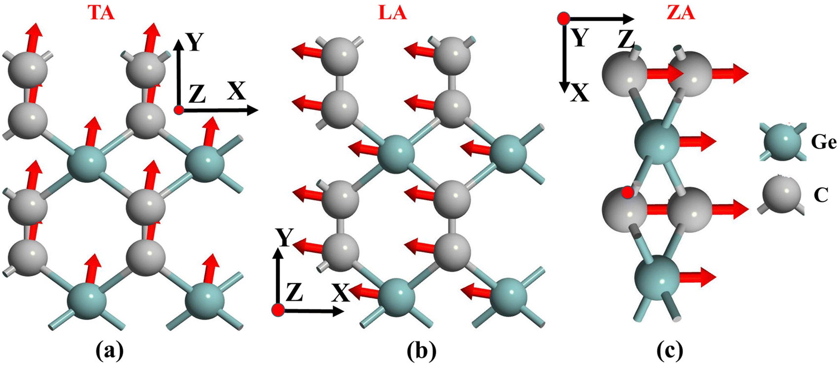
We further studied the electron mobility under three acoustic phonons’ scattering in the long-wave approximation (see Table S2, ESI† and Fig. 3). The ZA mode had the most significant effect on the mobility, limiting the intrinsic electron mobility to 2.8 × 103 cm2 (V s)−1. The LA mode was the next most influential factor, limiting the intrinsic electron mobility to 8.5 × 103 cm2 (V s)−1. This indicates that the DPT, which only considers scattering due to the LA phonon, is insufficient to predict electron mobility accurately. On the other hand, when the ZA mode scattering was eliminated, the intrinsic electron mobility could be increased to 1.33 × 103 cm2 (V s)−1 (Fig. 2(a)). This suggests that the electron mobility of tetrahex-GeC2 can be improved by suppressing the ZA mode vibrations. Therefore, we illustrate the vibrations of three acoustic modes (Fig. 4).
 |
| | Fig. 3 The electron mobility of ML tetrahex-GeC2 varies with the EF shift resulting from scattering by the three acoustic branches ZA, TA and LA. | |
 |
| | Fig. 4 Schematics of the vibrational modes of the three acoustic branches, (a) TA (b) LA and (c) ZA. The plane in which GeC2 located is the X–Y plane. The gray and blue-green spheres represent the C and Ge atoms, respectively. | |
The ZA mode corresponds to the lattice vibration direction perpendicular to the plane on which tetrahex-GeC2 is located (Fig. 4(c)). Therefore, in practical applications, the electron mobility can be enhanced by selecting an appropriate substrate or using a clamping material to make tetrahex-GeC2 interact with each other, thus suppressing the ZA mode vibration.
To gain insight into why the ZA mode has the most powerful suppression effect on the electron mobility among the three acoustic modes, we plotted the correlation between the electron–phonon coupling strength (represented by the matrix element) and q(qx, qy) of the TA, LA and ZA modes (Fig. 5). The ZA mode has the most robust coupling to the electronic state near the CBM as shown in Fig. 5(c), indicating that the ZA mode scatters the electrons the most and thus suppresses the mobility the most.
 |
| | Fig. 5 The relationship between the electron–phonon coupling matrix and q(qx, qy) of (a) TA, (b) LA and (c) ZA acoustic modes. | |
Performance of ML tetrahex-GeC2 n-type DG MOSFETs
Fig. 6 demonstrates that the model of a sub-10 nm DG ML tetrahex-GeC2 NMOSFET consists of heavily doped tetrahex-GeC2 as the source, drain, and ML intrinsic tetrahex-GeC2 as the channel. To ensure efficient carrier injection and minimize tunnelling leakage in the off-state, an optimized source and drain doping concentration (Ne) is essential. Fig. S2 (ESI†) reveals that the optimal doping concentration for the source/drain is 0.0102 e per atom. SiO2 is used as the gate dielectric for transistors with gate lengths ranging from 3 to 10 nm. Equivalent oxide thickness (EOT) and supply voltage (Vds) are adopted as the parameters from the ITRS 2013 edition for HP and LP applications of similar length nodes (Table 1). In the following discussion, the term ITRS is used to refer to the ITRS 2013 edition, as it is directly related to sub-10 nm gate lengths and has more rigorous standards than subsequent versions. This implies that if the transistor's performance metrics meet the standards of the ITRS 2013 edition, it can also meet the goals of IRDS 2021.72
 |
| | Fig. 6 Schematic structure of DG ML tetrahex-GeC2 NMOSFETs, where Lul, Lg and UL denote the channel length, gate length and underlap part, respectively. | |
Table 1 A comparison of the ballistic performance of DG ML tetrahex-GeC2 NMOSFETs against the ITRS requirements for HP and LP transistors spanning the 2022–2028 horizon in the ITRS
|
|
L
g (nm) |
L
ul (nm) |
EOT (nm) |
I
off (μA μm−1) |
SS (mV dec−1) |
I
on (μA μm−1) |
I
on/Ioff |
C
t
(fF μm−1) |
τ (ps) |
PDP (fJ μm−1) |
| LP |
3 |
0 |
4.5 |
— |
— |
— |
— |
— |
— |
— |
|
|
|
2 |
4.5 |
5 × 10⁻⁵ |
78 |
150. |
3.00 × 10⁶ |
0.092 |
0.613 |
0.059 |
|
|
5 |
0 |
4.5 |
5 × 10⁻⁵ |
170 |
6. |
1.22 × 10⁵ |
0.269 |
44.039 |
0.172 |
|
|
|
2 |
4.5 |
5 × 10⁻⁵ |
73 |
537 |
1.07 × 10⁷ |
0.169 |
0.314 |
0.108 |
|
|
7 |
0 |
4.9 |
4 × 10⁻⁵ |
120 |
1762 |
4.41 × 10⁷ |
0.444 |
0.252 |
0.307 |
|
|
9 |
0 |
5.5 |
2 × 10⁻⁵ |
53 |
1791 |
8.96 × 10⁷ |
0.518 |
0.289 |
0.378 |
| HP |
3 |
0 |
4.5 |
0.1 |
182 |
100 |
9.99 × 10³ |
0.174 |
1.740 |
0.111 |
|
|
|
2 |
4.5 |
0.1 |
101 |
1514 |
1.51 × 10⁴ |
0.108 |
0.071 |
0.069 |
|
|
5 |
0 |
4.5 |
0.1 |
148 |
2538 |
2.54 × 10⁴ |
0.365 |
0.144 |
0.233 |
|
|
|
2 |
4.5 |
0.1 |
80 |
1768 |
1.77 × 10⁴ |
0.174 |
0.098 |
0.111 |
|
|
7 |
0 |
4.9 |
0.1 |
138 |
2552 |
2.55 × 10⁴ |
0.441 |
0.173 |
0.304 |
|
|
9 |
0 |
5.5 |
0.1 |
69 |
2592 |
2.59 × 10⁴ |
0.587 |
0.227 |
0.429 |
| ITRS LP in 2028 |
5.9 |
|
4.1 |
5 × 10⁻⁵ |
— |
295 |
5.90 × 10⁶ |
0.690 |
1.493 |
0.280 |
| ITRS HP in 2028 |
5.1 |
|
4.1 |
0.1 |
— |
900 |
9.00 × 10³ |
0.600 |
0.423 |
0.240 |
| ITRS LP in 2026 |
7.0 |
|
4.5 |
4 × 10⁻⁵ |
— |
337 |
8.42 × 10⁶ |
0.770 |
1.514 |
0.340 |
| ITRS HP in 2024 |
7.3 |
|
4.9 |
0.1 |
— |
1170 |
1.17 × 10⁴ |
0.770 |
0.451 |
0.360 |
| ITRS HP in 2024 |
6.7 |
|
4.3 |
0.1 |
— |
1100 |
1.10 × 10⁴ |
0.720 |
0.446 |
0.330 |
| ITRS LP in 2023 |
9.3 |
|
5.1 |
2 × 10⁻⁵ |
— |
458 |
2.29 × 10⁷ |
0.950 |
1.474 |
0.480 |
| ITRS LP in 2024 |
8.5 |
|
4.9 |
2 × 10⁻⁵ |
— |
395 |
1.98 × 10⁵ |
0.890 |
1.557 |
0.420 |
| ITRS HP in 2022 |
8.8 |
|
5.4 |
0.1 |
— |
1350 |
1.35 × 10⁴ |
0.870 |
0.463 |
0.450 |
To maximize the performance, a symmetric UL layer is incorporated into the DG ML tetrahex-GeC2 NMOSFET. This UL layer comprises a dielectric layer and part of the channel layer. Previous studies have demonstrated that such a structure's ballisticity (defined as the current ratio in the scattering and ballistic limits) can exceed 88% for an effective channel length of 10 nm or less.67–69 Therefore, in this study, the gate length (Lg) was kept lower than 10 nm and the maximal Lul was maintained (10 nm −Lg)/2.
A. On-state current.
The Ion is an essential factor for logic transistors, especially in high-performance servers that require fast switching speeds. It is determined by the current on the transfer characteristic curve when the gate voltage is Vg(on) = Vg(off) + Vds, where Vg(on/off) is the gate voltage with the current in the on/off state (Ion/Ioff). According to ITRS, Vdd is set to 0.64 V, 0.69 V, and 0.73 V for Lg values of 5(3) nm, 7 nm, and 9 nm, respectively. For HP applications, Ioff is fixed at 0.1 μA μm−1, while for LP applications, Ioff is set to 5 × 10⁵ μA μm−1, 4 × 10⁵ μA μm−1, and 2 × 10⁵ μA μm−1 for Lg values of 5(3) nm, 7 nm, and 9 nm, respectively.
To estimate the magnitude of the Ion in the device, the current of the DG ML GeC2 NMOSFET must first reach Ioff to determine Vg(off). As illustrated in Fig. 7, all DG ML GeC2 NMOSFETs can satisfy the HP and LP Ioff requirements, except for the NMOSFET with a Lg of 3 nm with no UL, where the source leakage current is too high to meet the LP Ioff requirements for LP applications. The Lg of the 3 nm NMOSFET with a Lul of 2 nm has a steeper subthreshold region in the I–Vg curve, which enables it to meet the LP Ioff requirements. This is because the UL enlarges the channel length and reduces the leakage current. Our following discussion of Ion will focus on device configurations that meet the Ioff requirements.
 |
| | Fig. 7 The transfer characteristics of the DG ML tetrahex-GeC2 NMOSFETs with Lg values of (a) 3 nm (b) 5 nm (c) 7 nm and (d) 9 nm. The red and blue dashed lines represent the Ioff requirement per ITRS for HP and LP devices, respectively. | |
The Ion of DG ML GeC2 NMOSFETs can be determined once Vg(off) is known. To begin with, we will focus on the Ion of DG ML GeC2 NMOSFETs without UL. As shown in Fig. 7 and Table 1, for LP applications, the Ion is 6 μA μm−1, 1762 μA μm−1 and 1791 μA μm−1 for Lg values of 5 nm, 7 nm and 9 nm, respectively. Among them, Ion for both Lg values of 7 nm and 9 nm are 4–5 times the LP ITRS requirements for similar nodes. For HP applications, the Ion values for Lg values of 5 nm, 7 nm, and 9 nm are 2538 μA μm−1, 2552 μA μm−1, and 2592 μA μm−1, respectively, which are more than twice the similar node requirements of ITRS for HP applications.
We then further investigated the influence of UL on the Ion. As shown in Fig. S3(a) (ESI†), for HP applications, when Lg is 3 nm, the Ion increases from 100 μA μm−1 to 2538 μA μm−1 with a Lul of 2 nm, exceeding the ITRS requirement for HP applications by more than twice (900 μA μm−1 for the 3/5.1 nm node). For LP applications (Fig. S3(b), ESI†), when Lg is 5 nm, the Ion increases from 6 μA μm−1 to 536 μA μm−1 with a Lul of 2 nm, surpassing the ITRS requirement for LP applications by almost twice (295 μA μm−1 for the 5.9 nm node).
We further compared the Ion of sub-10 nm DG ML GeC2 NMOSFETs with the conventional 2D semiconductor NMOSFETs (Tables 1, 2 and Fig. 8), such as MoS2, which is commonly used experimentally, and other 2D materials, including Bi2O2Se, InSe, arsenene, antimonene, GeSe, and silicane. These materials are desirable channel materials because of their air stability and high carrier mobilities for upcoming FETs. Moreover, 2D silicane is compatible with mature silicon-based technologies, in addition to its air stability and high carrier mobilities. We also compared GeC2 NMOSFETs with advanced Si-based FETs, including Si nanowire FETs, Si FinFETs, and ETSOI FETs. Additionally, we examined the Ion of the GeC2 NMOSFETs in comparison to Carbon Nanotube (CNT) FETs and Gate All Around (GAA) CNT FETs as a potential and competitive semiconductor device material in the post-Moore's Law Era.
Table 2 For HP applications, several key device metrics for the upper limits of the ballistic performance in sub-10 nm DG ML NMOSFETs of Bi2O2Se,73 MoS2,73 InSe,74 arsenene,75,76 antimonene,75,76 GeSe (armchair)28 and silicane77 as well as other sub-10 nm gate-length technologies4,78–83
| HP |
|
L
g (nm) |
L
ul (nm) |
I
on (μA μm−1) |
PDP (fJ μm−1) |
τ (ps) |
| n-type ML Bi2O2Se |
|
8.8 |
0 |
3380 |
0.249 |
0.102 |
|
|
|
6.7 |
0 |
2126 |
0.18 |
0.126 |
|
|
|
5 |
2 |
2067 |
0.123 |
0.093 |
|
|
|
3 |
3 |
996 |
0.061 |
0.093 |
| n-type ML MoS2 |
|
9 |
0 |
230 |
0.172 |
3.509 |
|
|
|
5 |
2 |
473.34 |
0.195 |
1.287 |
|
|
|
3 |
2 |
519.48 |
0.126 |
0.126 |
| n-type ML InSe |
|
7 |
0 |
1497 |
0.096 |
0.09 |
|
|
|
5 |
0 |
1538 |
0.078 |
0.075 |
|
|
|
3 |
2 |
1468 |
0.039 |
0.048 |
| n-type ML arsenene |
|
10 |
0 |
2912 |
0.372 |
0.135 |
|
|
|
8.5 |
0 |
2941 |
0.216 |
0.096 |
|
|
|
6.4 |
0 |
2536 |
0.189 |
0.081 |
|
|
DFT-NEGF |
5 |
0 |
655 |
0.159 |
0.177 |
|
|
|
|
2 |
2030 |
0.096 |
0.051 |
| n-type ML antimonene |
|
5 |
0 |
614 |
— |
— |
|
|
|
|
2 |
728 |
— |
— |
| n-type ML GeSe (armchair) |
|
5 |
4 |
483 |
0.073 |
0.237 |
|
|
|
4 |
4 |
494 |
0.056 |
0.177 |
|
|
|
3 |
4 |
492 |
0.043 |
0.137 |
| n-type ML silicane |
|
5 |
4 |
1374 |
0.037 |
0.042 |
|
|
|
3 |
4 |
527 |
0.016 |
0.047 |
| GGA CNT |
|
5 |
1 |
1703 |
0.072 |
0.078 |
|
|
|
3 |
2 |
1347 |
0.051 |
0.042 |
|
|
| Si nanowire |
|
10 |
— |
522 |
0.345 |
0.66 |
|
|
|
5 |
— |
115 |
0.165 |
1.44 |
| Si Fin |
|
10 |
— |
446 |
0.546 |
1.02 |
|
|
Experiment |
5 |
— |
269 |
0.432 |
1.605 |
| ETSOI |
|
8 |
— |
340 |
0.948 |
1.86 |
| CNT FET |
|
9 |
0 |
630 |
0.552 |
0.174 |
|
|
|
5 |
— |
1412 |
0.138 |
0.078 |
 |
| | Fig. 8 A comparison of the Ion of (a) HP and (b) LP application concerning the gate length Lg for the optimal DG ML tetrahex-GeC2, Bi2O2Se, antimonene, GeSe (armchair), silicane, MoS2, InSe and arsenene NMOSFETs, based on the ab initio quantum transport simulations. | |
For LP applications, ML GeC2 NMOSFETs have the largest Ion among the listed devices at 5 nm ≤ Lg ≤ 9 nm nodes. As Lg increases from 5 nm to 7 nm, the Ion of the ML GeC2 NMOSFETs rises drastically to 1762 μA μm−1, surpassing those of InSe and arsenene by more than four and three times, respectively. For HP applications, the Ion magnitude of ML GeC2 NMOSFETs is 2–3 × 10³ μA μm−1 at 5 nm ≤ Lg ≤ 9 nm nodes, which is 1–2 times higher than the Ion requirement for similar nodes in ITRS HP, and much higher than 500 μA μm−1 of the most studied MoS2. It is also noteworthy that the Ion values of the ML GeC2 NMOSFETs are comparable to those of ML Arsenic and Bi2O2Se, which have the highest ionic content of the listed materials. Additionally, the Ion of the ML GeC2 NMOSFETs is greater than those of the advanced silicon-based FETs, including Si nanowires, Si Fin, ETSOI, and CNT FETs at comparable nodes.
B. Gate control.
In addition to Ion, SS is a significant factor for evaluating device performance, showing its ability to manipulate the subthreshold domain's gate voltage. SS is determined using the following formula:| |  | (13) |
where Id is the source–drain current, and a smaller SS indicates a better gating capability and usually a larger Ion current. At room temperature, 60 mV dec−1 is the Boltzmann limit, which is the fundamental thermal limit of SS in NMOSFETs.84 The SS can be determined by the steepest point of the transfer characteristic curve at Vg when the current consists of tunneling and thermionic components (Id = Itunnel + Itherm):67| |  | (14) |
| |  | (15) |
When rtunnel = 0, the current is thermionic and SS is equal to SStherm with a fundamental limit of 60 mV dec−1. However, when 0 < rtunnel <1, the Itunnel must be considered, causing SS to be less than 60 mV dec−1. As shown in Fig. 9 and Table 1, for the HP application, the SS values of the 3 nm and 5 nm DG ML GeC2 NMOSFETs with a Lul of 2 nm reduce to 78 mV dec−1 and 73 mV dec−1, respectively. While the 9 nm one without UL has an SS value of 69 mV dec−1. These values are close to the desired value of 60 mV dec−1. As previously mentioned, the UL widens the barrier and effective channel length, thus reducing the short-channel effect, steepening the slope of the transfer curve, and lowering the SS values. For LP applications, the 9 nm DG ML GeC2 NMOSFET has the lowest SS value of 53 mV dec−1 among the GeC2 NMOSFETs, which is below the fundamental limit of 60 mV dec−1 and also lower than the 60 mV dec−1 value of 9 nm DG ML Bi2O2Se.73
 |
| | Fig. 9 SS as a function of gate length Lg for DG ML GeC2 NMOSFETs with and without UL. The black dashed lines indicate the Boltzmann limit of 60 mV dec−1 for SS at room temperature. | |
To understand why SS can be taken below 60 mV dec−1 in LP applications, we have calculated the spectral currents and local density of states (LDOS) for the three Vg values of −0.4 V, −0.1 V, and 0.2 V at a Lg of 9 nm with a step change of 0.2 V (Fig. 10) The SS at −0.4 V is near its minimum value, while the SS at 0.2 V is much higher than 60 mV dec−1, and the SS at −0.1 V falls in between. As shown in Fig. 10, the Itunnel current is a major component of the total current when Vg = −0.4 V, which is nearly 50%, thus 0 < rtunnel < 1. At Vg = 0.2 V, almost all of the current is Itherm and the rtunnel is almost zero. The tunneling potential and Itunnel are related using the following formula:85
| |  | (16) |
where
ϕB and
w are the height and width of the potential barrier, respectively. As the potential width
w remains constant, the
Itunnel is mainly determined by the potential barrier height
ϕB. When
Vg is changed from −0.4 V to −0.1 V,
ϕB decreases by 0.256 eV, whereas when
Vg is varied from −0.1 V to 0.2 V, the decrease in
ϕB is only 0.032 eV. This indicates that when
Vg is −0.4 V, the rate of change of the potential barrier is high, thus resulting in a large rate of change of
Itunnel. This means that the SS
tunnel is low enough to meet the requirement of SS
tunnel < SS
therm.
 |
| | Fig. 10 Spatially resolved LDOS and spectral currents of the 9 nm DG ML GeC2 NMOSFET at Vg of (a) −0.4 V, (b) −0.1 V and (c) 0.2 V, respectively. The electrochemical potentials of the source and drain are denoted as εL and εR, respectively, while ϕB is the energy barrier for electrons at the CBM transporting from the drain to the source. | |
Transconductance gm is a key indicator of device performance, indicating the gate control capability in the superthreshold region, and gm is calculated as follows:86
| |  | (17) |
A large
gm implies better gate control and a higher
Ion. As shown in
Fig. 11, for HP/LP applications, 3 nm, 5 nm, 7 nm and 9 nm DG ML GeC
2 NMOSFETs have
gm of 4.51–13.16 mS μm
−1, which is similar to the 7–12 mS μm
−1 of Bi
2O
2Se NMOSFETs.
52 It should be noted that when a 2 nm UL is used, the
gm will be reduced in the superthreshold region.
 |
| | Fig. 11 The gm of DG ML GeC2 NMOSFETs with and without ULs as a function of the gate length Lg in the HP and LP applications. | |
C. Intrinsic delay time and power consumption.
The switching speed is an important quality factor for digital circuits, usually measured by the intrinsic delay time τ. A lower τ implies faster switching speeds. It is calculated by applying the following equation:86| |  | (18) |
where Vds is the source–drain voltage, and the ITRS standard states that the total gate capacitance Ct is three times the intrinsic channel capacitance, that is Ct = 3 Cg. Cg is expressed as:4,86,87| |  | (19) |
Q is the total channel charge. Table 1, Fig. S4 and S5 (ESI†) detail the performance metrics gate capacitance (Ct), delay times (τ) and the power dissipation per unit width (PDP) of DG ML GeC2 NMOSFETs Ct ranges from 0.092 to 0.518/0.108 to 0.587 fF μm−1 for HP/LP applications, respectively, aligning with ITRS standards and indicating optimal interface capacitance. τ values range from 0.07 to 0.23 ps/0.25 to 0.61 ps (except for Lg = 3 nm with the UL configuration) for HP/LP applications, which are significantly below the ITRS upper limits of 0.69–0.95 ps and 0.60–0.87 ps, respectively, demonstrating high switching speeds. In Tables 2, 3 and Fig. S6 (ESI†), we compare τ of DG ML GeC2 NMOSFETs with other DG ML NMOSFETs. For HP applications, GeC2 shows a significantly lower τ than MoS2 and is comparable to Bi2O2Se, InSe, Arsenene, silicane, and GeSe. For LP applications, GeC2's τ is notably smaller than MoS2's, aligning closely with InSe and Arsenene. The PDP (PDP = CtVds2) for these FETs ranges from 0.059 to 0.306/0.069 to 0.428 fJ μm−1 for LP/HP applications, lower than the ITRS standard upper limits. Furthermore, as Tables 2, 3 and Fig. S7 (ESI†) show that the PDP of DG ML GeC2 NMOSFETs is comparable to those of Bi2O2Se, MoS2, InSe, and arsenene NMOSFETs. These performances suggest that DG ML GeC2 NMOSFETs are competitive with other 2D materials, offering both low delay time and low power consumption.
Table 3 For LP applications, several key device metrics for the ballistic performance upper limits of the sub-10 nm DG ML NMOSFETs of Bi2O2Se,73 MoS2,73 InSe,74 arsenene,75,76 antimonene75,76 and GeSe (armchair)28
| LP |
|
L
g (nm) |
L
ul (nm) |
I
on (μA μm−1) |
PDP (fJ μm−1) |
τ (ps) |
| n-type ML Bi2O2Se |
DFT+NEGF |
9.3 |
0 |
10 |
0.408 |
57.5 |
|
|
7.0 |
0 |
3.8 × 10⁻³ |
0.340 |
1.4 × 10⁵ |
|
|
5.0 |
2 |
4.1 × 10⁻³ |
0.258 |
9.8 × 10⁴ |
| n-type ML MoS2 |
5 |
3 |
324.05 |
0.093 |
0.552 |
|
|
3 |
2 |
133.09 |
0.078 |
2.337 |
| n-type ML InSe |
7 |
0 |
401 |
0.078 |
0.339 |
|
|
5 |
2 |
424 |
0.039 |
0.210 |
|
|
3 |
3 |
69 |
0.03 |
0.852 |
| n-type ML arsenene |
10 |
0 |
1750 |
0.411 |
0.225 |
|
|
8.5 |
0 |
1325 |
0.15 |
0.213 |
|
|
6.4 |
0 |
560 |
0.096 |
0.267 |
|
|
5 |
0 |
152 |
0.156 |
0.759 |
|
|
|
2 |
341 |
0.069 |
0.303 |
| n-type ML antimonene |
5 |
0 |
42.8 |
— |
— |
|
|
|
2 |
482 |
— |
— |
| n-type ML GeSe (zigzag) |
5 |
4 |
274 |
0.055 |
0.320 |
|
|
4 |
4 |
161 |
0.05 |
0.480 |
|
|
3 |
4 |
6.7 |
0.047 |
10.99 |
| n-type ML silicane |
5 |
4 |
438 |
0.021 |
0.073 |
|
|
3 |
4 |
467 |
0.016 |
0.054 |
Conclusions
Our research revealed that ML tetrahex-GeC2 is a potential channel material for sub-10 nm NMOSFETs due to its high electron mobility and superior electrical performance when compared to other 2D semiconductors. Using the linearized BTE with normalized full-band RTA and DFT, we calculated the electron mobility of ML tetrahex-GeC2 to be 803 cm2 (V s)−1 at 300 K, which is much higher than the electron mobility of MoS2, which was assessed to be 400 cm2 (V s)−1 using the same method and measured experimentally. Contrary to the DPT's suggestion, the ZA acoustic mode was determined to be the most restrictive for the electron mobility, not the LA phonon. Ab initio quantum transport simulations were used to assess the performance of sub-10 nm DG ML tetrahex-GeC2 NMOSFETs with Lg values of 3 nm, 5 nm, 7 nm, and 9 nm. The UL effect was considered for the first two lengths. The study found that these NMOSFETs can meet the requirements of the ITRS for both HP and LP applications. Particularly for HP, the Ion is comparable to those of Bi2O2Se and arsenene and better than that of MoS2. For LP, Ion surpasses that of arsenene at Lg values of 7 nm and 9 nm. The SS demonstrates excellent gate control capability, with values as low as 69/53 mV dec−1 for HP/LP at Lg values of 9 nm and 73 mV dec−1 at the Lg of 5 nm for LP. Delay times τ for all Lg are within ITRS limits and are comparable to other notable materials like InSe, arsenene, Bi2O2Se, and silicane. The power dissipation PDP at Lg also remains below the upper limits of ITRS, and the performance for HP and LP applications is comparable with that of materials like Bi2O2Se, MoS2, arsenene, InSe, and GeSe. Overall, this study shows the promising potential of sub-10 nm DG ML tetrahex-GeC2 NMOSFETs in both HP and LP applications.
Data availability statements
All data that support the findings of this study are included within the article (and in the ESI†).
Conflicts of interest
There are no conflicts to declare.
Acknowledgements
Calculations were carried out in the High-Performance Computing Laboratory of Changzhou University and at the Hefei Advanced Computing Center. Literature analysis is performed using the Stork software (https://www.storkapp.me).
Notes and references
- S. Wang, X. Liu and P. Zhou, The Road for 2D Semiconductors in the Silicon Age, Adv. Mater., 2022, 34(48), 2106886, DOI:10.1002/adma.202106886.
- Y. Liu, X. Duan, H.-J. Shin, S. Park, Y. Huang and X. Duan, Promises and prospects of two-dimensional transistors, Nature, 2021, 591(7848), 43–53, DOI:10.1038/s41586-021-03339-z.
- S. B. Mitta, M. S. Choi, A. Nipane, F. Ali, C. Kim, J. T. Teherani, J. Hone and W. J. Yoo, Electrical characterization of 2D materials-based field-effect transistors, 2D Mater., 2021, 8(1), 012002, DOI:10.1088/2053-1583/abc187.
- R. Quhe, L. Xu, S. Liu, C. Yang, Y. Wang, H. Li, J. Yang, Q. Li, B. Shi and Y. Li,
et al., Sub-10 nm two-dimensional transistors: Theory and experiment, Phys. Rep., 2021, 938, 1–72, DOI:10.1016/j.physrep.2021.07.006.
- D. W. Kim, S. Y. Min, Y. Lee and U. Jeong, Transparent Flexible Nanoline Field-Effect Transistor Array with High Integration in a Large Area, ACS Nano, 2020, 14(1), 907–918, DOI:10.1021/acsnano.9b08199 From NLM PubMed-not-MEDLINE.
- A. Pramanik, S. Biswas, S. Pal and P. Sarkar, Charge transport and transfer phenomena involving conjugated acenes and heteroacenes, Bull. Mater. Sci., 2019, 42, 1–20 CrossRef CAS.
- A. Pramanik, B. Mandal, S. Sarkar and P. Sarkar, Effect of edge states on the transport properties of pentacene–graphene nanojunctions, Chem. Phys. Lett., 2014, 597, 1–5 CrossRef CAS.
- Y. Kimura, M. Niwano, N. Ikuma, K. Goushi and K. Itaya, Organic field effect transistor using pentacene single crystals grown by a liquid-phase crystallization process, Langmuir, 2009, 25(9), 4861–4863 CrossRef CAS PubMed.
- M. Ahles, R. Schmechel and H. von Seggern, N-type organic field-effect transistor based on interface-doped pentacene, Appl. Phys. Lett., 2004, 85(19), 4499–4501 CrossRef CAS.
- V. Y. Butko, X. Chi, D. V. Lang and A. P. Ramirez, Field-effect transistor on pentacene single crystal, Appl. Phys. Lett., 2003, 83(23), 4773–4775 CrossRef CAS.
- P. Wang, S. Han and R. Quhe, Quantum transport simulation of the two-dimensional GaSb transistors, J. Semicond., 2021, 42(12), 122001, DOI:10.1088/1674-4926/42/12/122001.
- C. Tantardini, A. G. Kvashnin, C. Gatti, B. I. Yakobson and X. Gonze, Computational Modeling of 2D Materials under High Pressure and Their Chemical Bonding: Silicene as Possible Field-Effect Transistor, ACS Nano, 2021, 15(4), 6861–6871, DOI:10.1021/acsnano.0c10609.
- J. Chen, H. Pu, M. C. Hersam and P. Westerhoff, Molecular Engineering of 2D Nanomaterial Field-Effect Transistor Sensors: Fundamentals and Translation across the Innovation Spectrum, Adv. Mater., 2022, 34(3), e2106975, DOI:10.1002/adma.202106975.
- C. Dai, Y. Liu and D. Wei, Two-Dimensional Field-Effect Transistor Sensors: The Road toward Commercialization, Chem. Rev., 2022, 122(11), 10319–10392, DOI:10.1021/acs.chemrev.1c00924.
- J. Jiang, L. Xu, C. Qiu and L. M. Peng, Ballistic two-dimensional InSe transistors, Nature, 2023, 616(7957), 470–475, DOI:10.1038/s41586-023-05819-w.
- C. Tan, M. Yu, J. Tang, X. Gao, Y. Yin, Y. Zhang, J. Wang, X. Gao, C. Zhang and X. Zhou,
et al., 2D fin field-effect transistors integrated with epitaxial high-k gate oxide, Nature, 2023, 616(7955), 66–72, DOI:10.1038/s41586-023-05797-z.
- Y. Xu, J. Dai and X. C. Zeng, Al2C Monolayer Sheet and Nanoribbons with Unique Direction-Dependent Acoustic-Phonon-Limited Carrier Mobility and Carrier Polarity, J. Phys. Chem. Lett., 2016, 7(2), 302–307, DOI:10.1021/acs.jpclett.5b02695.
- G. Fiori, F. Bonaccorso, G. Iannaccone, T. Palacios, D. Neumaier, A. Seabaugh, S. K. Banerjee and L. Colombo, Electronics based on two-dimensional materials, Nat. Nanotechnol., 2014, 9(10), 768–779, DOI:10.1038/nnano.2014.207.
- Y. Xiao, C. Xiong, M. M. Chen, S. Wang, L. Fu and X. Zhang, Structure modulation of two-dimensional transition metal chalcogenides: recent advances in methodology, mechanism and applications, Chem. Soc. Rev., 2023, 52(4), 1215–1272, 10.1039/d1cs01016f.
- L. Xie, M. Liao, S. Wang, H. Yu, L. Du, J. Tang, J. Zhao, J. Zhang, P. Chen and X. Lu, Graphene-contacted ultrashort channel monolayer MoS2 transistors, Adv. Mater., 2017, 29(37), 1702522 CrossRef PubMed.
- A. Nourbakhsh, A. Zubair, R. N. Sajjad, A. Tavakkoli KG, W. Chen, S. Fang, X. Ling, J. Kong, M. S. Dresselhaus and E. Kaxiras, MoS2 field-effect transistor with sub-10 nm channel length, Nano Lett., 2016, 16(12), 7798–7806 CrossRef CAS PubMed.
- K. Xu, D. Chen, F. Yang, Z. Wang, L. Yin, F. Wang, R. Cheng, K. Liu, J. Xiong and Q. Liu, Sub-10 nm nanopattern architecture for 2D material field-effect transistors, Nano Lett., 2017, 17(2), 1065–1070 CrossRef CAS PubMed.
-
L. Wilson, International technology roadmap for semiconductors (ITRS), Semiconductor Industry Association, 2013, vol. 2013 Search PubMed.
- Y. Xu, J. Dai and X. C. Zeng, Electron-Transport Properties of Few-Layer Black Phosphorus, J. Phys. Chem. Lett., 2015, 6(11), 1996–2002, DOI:10.1021/acs.jpclett.5b00510.
- H. Liu, A. T. Neal, Z. Zhu, Z. Luo, X. Xu, D. Tománek and P. D. Ye, Phosphorene: an unexplored 2D semiconductor with a high hole mobility, ACS Nano, 2014, 8(4), 4033–4041 CrossRef CAS PubMed.
- M. Batmunkh, M. Bat-Erdene and J. G. Shapter, Phosphorene and Phosphorene-Based Materials - Prospects for Future Applications, Adv. Mater., 2016, 28(39), 8586–8617 CrossRef CAS PubMed.
- Y. Du, H. Liu, Y. Deng and P. D. Ye, Device perspective for black phosphorus field-effect transistors: contact resistance, ambipolar behavior, and scaling, ACS Nano, 2014, 8(10), 10035–10042 CrossRef CAS PubMed.
- Y. Guo, F. Pan, G. Zhao, Y. Ren, B. Yao, H. Li and J. Lu, Sub-5 nm monolayer germanium selenide (GeSe) MOSFETs: towards a high performance and stable device, Nanoscale, 2020, 12(28), 15443–15452, 10.1039/d0nr02170a.
- Y. Ma, C. Shen, A. Zhang, L. Chen, Y. Liu, J. Chen, Q. Liu, Z. Li, M. R. Amer and T. Nilges,
et al., Black Phosphorus Field-Effect Transistors with Work Function Tunable Contacts, ACS Nano, 2017, 11(7), 7126–7133, DOI:10.1021/acsnano.7b02858.
- A. Pon, A. Bhattacharyya and R. Rathinam, Recent Developments in Black Phosphorous Transistors: A Review, J. Electron. Mater., 2021, 50(11), 6020–6036, DOI:10.1007/s11664-021-09183-1.
- J. Zhang, L. Liu, Y. Yang, Q. Huang, D. Li and D. Zeng, A review on two-dimensional materials for chemiresistive- and FET-type gas sensors, Phys. Chem. Chem. Phys., 2021, 23(29), 15420–15439 RSC.
- H. Li, B. Shi, Y. Pan, J. Li, L. Xu, L. Xu, Z. Zhang, F. Pan and J. Lu, Sub-5 nm monolayer black phosphorene tunneling transistors, Nanotechnology, 2018, 29(48), 485202 CrossRef PubMed.
- Z. Chen, Gate-all-around nanosheet transistors go 2D, Nat. Electron., 2022, 5(12), 830–831 CrossRef.
- J. Na, M.-K. Joo, M. Shin, J. Huh, J.-S. Kim, M. Piao, J.-E. Jin, H.-K. Jang, H. J. Choi and J. H. Shim, Low-frequency noise in multilayer MoS 2 field-effect transistors: the effect of high-k passivation, Nanoscale, 2014, 6(1), 433–441 RSC.
- S. Sharma, S. Das, R. Khosla, H. Shrimali and S. K. Sharma, Two-dimensional van der Waals hafnium disulfide and zirconium oxide-based micro-interdigitated electrodes transistors, IEEE Trans. Electron Devices, 2022, 70(4), 1520–1526 Search PubMed.
- F. Xu, Z. Wu, G. Liu, F. Chen, J. Guo, H. Zhou, J. Huang, Z. Zhang, L. Fei and X. Liao, Few-layered MnAl2S4 dielectrics for high-performance van der Waals stacked transistors, ACS Appl. Mater. Interfaces, 2022, 14(22), 25920–25927 CrossRef CAS PubMed.
- J. Su, G. Chen, W. Wang, H. Shi, S. He, X. Lv, Y. Wang, M. Zhang, R. Wang and H.-X. Wang, Electrical characteristics of normally off hydrogen-terminated diamond field effect transistors with lanthanum oxide gate dielectric, Appl. Phys. Lett., 2022, 121(16), 162103 CrossRef CAS.
- J. Ma, X. Chen, X. Wang, J. Bian, L. Tong, H. Chen, X. Guo, Y. Xia, X. Zhang and Z. Xu, Engineering top gate stack for wafer-scale integrated circuit fabrication based on two-dimensional semiconductors, ACS Appl. Mater. Interfaces, 2022, 14(9), 11610–11618 CrossRef CAS PubMed.
- P. Singh, S. Baek, H. H. Yoo, J. Niu, J.-H. Park and S. Lee, Two-dimensional CIPS-InSe van der Waals heterostructure ferroelectric field effect transistor for nonvolatile memory applications, ACS Nano, 2022, 16(4), 5418–5426 CrossRef CAS PubMed.
- S. Moon, D. Lee, J. Park and J. Kim, 2D Amorphous GaOX Gate Dielectric for β-Ga2O3 Field-Effect Transistors, ACS Appl. Mater. Interfaces, 2023, 15(31), 37687–37695 CrossRef CAS PubMed.
- J. Jadwiszczak, J. Sherman, D. Lynall, Y. Liu, B. Penkov, E. Young, R. Keneipp, M. Drndić, J. C. Hone and K. L. Shepard, Mixed-dimensional 1D/2D van der Waals heterojunction diodes and transistors in the atomic limit, ACS Nano, 2022, 16(1), 1639–1648 CrossRef CAS PubMed.
- J. Ma, X. Chen, Y. Sheng, L. Tong, X. Guo, M. Zhang, C. Luo, L. Zong, Y. Xia and C. Sheng, Top gate engineering of field-effect transistors based on wafer-scale two-dimensional semiconductors, J. Mater. Sci. Technol., 2022, 106, 243–248 CrossRef CAS.
- K.-H. Kim, S. Oh, M. M. A. Fiagbenu, J. Zheng, P. Musavigharavi, P. Kumar, N. Trainor, A. Aljarb, Y. Wan and H. M. Kim, Scalable CMOS back-end-of-line-compatible AlScN/two-dimensional channel ferroelectric field-effect transistors, Nat. Nanotechnol., 2023, 1–7 Search PubMed.
- J.-K. Huang, Y. Wan, J. Shi, J. Zhang, Z. Wang, W. Wang, N. Yang, Y. Liu, C.-H. Lin and X. Guan, High-κ perovskite membranes as insulators for two-dimensional transistors, Nature, 2022, 605(7909), 262–267 CrossRef CAS PubMed.
- Y. Xu, T. Liu, K. Liu, Y. Zhao, L. Liu, P. Li, A. Nie, L. Liu, J. Yu and X. Feng, Scalable integration of hybrid high-κ dielectric materials on two-dimensional semiconductors, Nat. Mater., 2023, 1–7 Search PubMed.
- J. Chen, Z. Liu, X. Dong, Z. Gao, Y. Lin, Y. He, Y. Duan, T. Cheng, Z. Zhou and H. Fu, Vertically grown ultrathin Bi2SiO5 as high-κ single-crystalline gate dielectric, Nat. Commun., 2023, 14(1), 4406 CrossRef CAS PubMed.
- S. Banerjee, L. Cao, Y. S. Ang, L. K. Ang and P. Zhang, Reducing Contact Resistance in Two-Dimensional-Material-Based Electrical Contacts by Roughness Engineering, Phys. Rev. Appl., 2020, 13(6), 064021, DOI:10.1103/PhysRevApplied.13.064021.
-
W. Park, Y. Kim, L. Sang Kyung, U. Jung, Y. Jin Ho, C. Cho, K. Yun Ji, L. Sung Kwan, H. In Seol, H. B. R. Lee, et al., Contact resistance reduction using Fermi level de-pinning layer for MoS2 FETs, 2014 IEEE International Electron Devices Meeting, 15–17 December 2014, 2014, pp. 5.1.1–5.1.4 DOI:10.1109/IEDM.2014.7046986.
- S. Lin, Y. Guo, M. Xu, J. Zhao, Y. Liang, X. Yuan, Y. Zhang, F. Wang, J. Hao and Y. Li, AB 2 N monolayer: a direct band gap semiconductor with high and highly anisotropic carrier mobility, Nanoscale, 2022, 14(3), 930–938 RSC.
- W. Shangguan, C. Yan, W. Li, C. Long, L. Liu, C. Qi, Q. Li, Y. Zhou, Y. Guan and L. Gao, Two-dimensional semiconductor materials with high stability and electron mobility in group-11 chalcogenide compounds: MNX (M = Cu, Ag, Au; N = Cu, Ag, Au; X = S, Se, Te; M ≠ N), Nanoscale, 2022, 14(11), 4271–4280 RSC.
- Y. Guo, Q. Wu, Y. Li, N. Lu, K. Mao, Y. Bai, J. Zhao, J. Wang and X. C. Zeng, Copper (i) sulfide: a two-dimensional semiconductor with superior oxidation resistance and high carrier mobility, Nanoscale Horiz., 2019, 4(1), 223–230 RSC.
- R. Quhe, J. Liu, J. Wu, J. Yang, Y. Wang, Q. Li, T. Li, Y. Guo, J. Yang and H. Peng, High-performance sub-10 nm monolayer Bi2O2Se transistors, Nanoscale, 2019, 11(2), 532–540 RSC.
- W. Zhang, C. Chai, Q. Fan, M. Sun, Y. Song, Y. Yang and U. Schwingenschlögl, Two-Dimensional Tetrahex-GeC2: A Material with Tunable Electronic and Optical Properties Combined with Ultrahigh Carrier Mobility, ACS Appl. Mater. Interfaces, 2021, 13(12), 14489–14496, DOI:10.1021/acsami.0c23017.
- W. Zhang, C. Chai, Q. Fan, M. Sun, Y. Song, Y. Yang and U. Schwingenschlögl, Two-Dimensional Tetrahex-GeC2: A Material with Tunable Electronic and Optical Properties Combined with Ultrahigh Carrier Mobility, J. Phys. Chem. Lett., 2021, 13(12), 14489–14496, DOI:10.1021/acsami.0c23017.
- L. Cheng, C. Zhang and Y. Liu, The Optimal Electronic Structure for High-Mobility 2D Semiconductors: Exceptionally High Hole Mobility in 2D Antimony, J. Am. Chem. Soc., 2019, 141(41), 16296–16302, DOI:10.1021/jacs.9b05923.
- L. Cheng, C. Zhang and Y. Liu, Why Two-Dimensional Semiconductors Generally Have Low Electron Mobility, Phys. Rev. Lett., 2020, 125(17), 177701, DOI:10.1103/PhysRevLett.125.177701.
- H. Lang, S. Zhang and Z. Liu, Mobility anisotropy of two-dimensional semiconductors, Phys. Rev. B, 2016, 94(23), 235306, DOI:10.1103/PhysRevB.94.235306.
- T. Gunst, T. Markussen, K. Stokbro and M. Brandbyge, First-principles method for electron-phonon coupling and electron mobility: Applications to two-dimensional materials, Phys. Rev. B, 2016, 93(3), 035414, DOI:10.1103/PhysRevB.93.035414.
- M. V. Fischetti and S. E. Laux, Band structure, deformation potentials, and carrier mobility in strained Si, Ge, and SiGe alloys, J. Appl. Phys., 1996, 80(4), 2234–2252 CrossRef CAS.
- S. D. Sarma, S. Adam, E. H. Hwang and E. Rossi, Electronic transport in two-dimensional graphene, Rev. Mod. Phys., 2011, 83(2), 407 CrossRef.
- T. Kawamura and S. D. Sarma, Phonon-scattering-limited electron mobilities in Al x Ga 1− x As/GaAs heterojunctions, Phys. Rev. B: Condens. Matter Mater. Phys., 1992, 45(7), 3612 CrossRef CAS PubMed.
- T. Sohier, M. Calandra, C.-H. Park, N. Bonini, N. Marzari and F. Mauri, Phonon-limited resistivity of graphene by first-principles calculations: Electron-phonon interactions, strain-induced gauge field, and Boltzmann equation, Phys. Rev. B: Condens. Matter Mater. Phys., 2014, 90(12), 125414 CrossRef.
-
G. D. Mahan, Many-particle physics, Springer Science & Business Media, 2000 Search PubMed.
- S. Smidstrup, T. Markussen, P. Vancraeyveld, J. Wellendorff, J. Schneider, T. Gunst, B. Verstichel, D. Stradi, P. A. Khomyakov and U. G. Vej-Hansen, QuantumATK: An integrated platform of electronic and atomic-scale modelling tools, J. Phys.: Condens. Matter, 2019, 32(1), 015901 CrossRef PubMed.
- F. Tran and P. Blaha, Accurate Band Gaps of Semiconductors and Insulators with a Semilocal Exchange-Correlation Potential, Phys. Rev. Lett., 2009, 102(22), 226401, DOI:10.1103/PhysRevLett.102.226401.
- M. J. van Setten, M. Giantomassi, E. Bousquet, M. J. Verstraete, D. R. Hamann, X. Gonze and G. M. Rignanese, The PseudoDojo: Training and grading a 85 element optimized norm-conserving pseudopotential table, Comput. Phys. Commun., 2018, 226, 39–54, DOI:10.1016/j.cpc.2018.01.012.
- R. Quhe, Q. Li, Q. Zhang, Y. Wang, H. Zhang, J. Li, X. Zhang, D. Chen, K. Liu and Y. Ye,
et al., Simulations of Quantum Transport in Sub-5-nm Monolayer Phosphorene Transistors, Phys. Rev. Appl., 2018, 10(2), 024022, DOI:10.1103/PhysRevApplied.10.024022.
- K. T. Lam, Z. Dong and J. Guo, Performance Limits Projection of Black Phosphorous Field-Effect Transistors, IEEE Electron Device Lett., 2014, 35(9), 963–965, DOI:10.1109/LED.2014.2333368.
- L. Liu, Y. Lu and J. Guo, On Monolayer MoS2 Field-Effect Transistors at the Scaling Limit, IEEE Trans. Electron Devices, 2013, 60(12), 4133–4139, DOI:10.1109/TED.2013.2284591.
-
S. Datta, Electronic transport in mesoscopic systems, Cambridge University Press, 1997 Search PubMed.
- P. Sang, Q. Wang, W. Wei, F. Wang, Y. Li and J. Chen, Semiconducting Silicene: A Two-Dimensional Silicon Allotrope with Hybrid Honeycomb-Kagome Lattice, ACS Mater. Lett., 2021, 3(8), 1181–1188, DOI:10.1021/acsmaterialslett.1c00259.
- Q. Li, S. Fang, S. Liu, L. Xu, L. Xu, C. Yang, J. Yang, B. Shi, J. Ma and J. Yang,
et al., Performance Limit of Ultrathin GaAs Transistors, ACS Appl. Mater. Interfaces, 2022, 14(20), 23597–23609, DOI:10.1021/acsami.2c01134.
- R. Quhe, J. Liu, J. Wu, J. Yang, Y. Wang, Q. Li, T. Li, Y. Guo, J. Yang and H. Peng,
et al., High-performance sub-10 nm monolayer Bi2O2Se transistors, Nanoscale, 2019, 11(2), 532–540, 10.1039/c8nr08852g.
- Y. Wang, R. Fei, R. Quhe, J. Li, H. Zhang, X. Zhang, B. Shi, L. Xiao, Z. Song and J. Yang,
et al., Many-Body Effect and Device Performance Limit of Monolayer InSe, ACS Appl. Mater. Interfaces, 2018, 10(27), 23344–23352, DOI:10.1021/acsami.8b06427.
- Y. Wang, P. Huang, M. Ye, R. Quhe, Y. Pan, H. Zhang, H. Zhong, J. Shi and J. Lu, Many-body Effect, Carrier Mobility, and Device Performance of Hexagonal Arsenene and Antimonene, Chem. Mater., 2017, 29(5), 2191–2201, DOI:10.1021/acs.chemmater.6b04909.
- X. Sun, Z. Song, S. Liu, Y. Wang, Y. Li, W. Wang and J. Lu, Sub-5 nm Monolayer Arsenene and Antimonene Transistors, ACS Appl. Mater. Interfaces, 2018, 10(26), 22363–22371, DOI:10.1021/acsami.8b03840.
- Y. Pan, J. Dai, L. Xu, J. Yang, X. Zhang, J. Yan, J. Li, B. Shi, S. Liu and H. Hu,
et al., Sub-5-nm Monolayer Silicane Transistor: A First-Principles Quantum Transport Simulation, Phys. Rev. Appl., 2020, 14(2), 024016, DOI:10.1103/PhysRevApplied.14.024016.
-
F.-L. Yang, D.-H. Lee, H.-Y. Chen, C.-Y. Chang, S.-D. Liu, C.-C. Huang, T.-X. Chung, H.-W. Chen, C.-C. Huang and Y.-H. Liu, 5nm-gate nanowire FinFET, Digest of Technical Papers. 2004 Symposium on VLSI Technology, 2004, 2004, IEEE, pp. 196–197.
-
B. Yu, L. Chang, S. Ahmed, H. Wang, S. Bell, C.-Y. Yang, C. Tabery, C. Ho, Q. Xiang and T.-J. King, FinFET scaling to 10 nm gate length, Digest. International Electron Devices Meeting, IEEE, 2002, pp. 251–254.
-
H. Lee, L.-E. Yu, S.-W. Ryu, J.-W. Han, K. Jeon, D.-Y. Jang, K.-H. Kim, J. Lee, J.-H. Kim and S. Jeon, Sub-5nm all-around gate FinFET for ultimate scaling, 2006 Symposium on VLSI Technology, 2006. Digest of Technical Papers, IEEE, 2006, pp. 58–59.
-
B. Doris, M. Ieong, T. Zhu, Y. Zhang, M. Steen, W. Natzle, S. Callegari, V. Narayanan, J. Cai and S. Ku, Device design considerations for ultra-thin SOI MOSFETs, IEEE International Electron Devices Meeting 2003, IEEE, 2003, pp. 27.23.21–27.23.24.
- A. D. Franklin, M. Luisier, S.-J. Han, G. Tulevski, C. M. Breslin, L. Gignac, M. S. Lundstrom and W. Haensch, Sub-10 nm carbon nanotube transistor, Nano Lett., 2012, 12(2), 758–762 CrossRef CAS PubMed.
- C. Qiu, Z. Zhang, M. Xiao, Y. Yang, D. Zhong and L.-M. Peng, Scaling carbon nanotube complementary transistors to 5-nm gate lengths, Science, 2017, 355(6322), 271–276 CrossRef CAS PubMed.
- S. Wang, J. Wang, T. Zhi, J. Xue, D. Chen, L. Wang and R. Zhang, Cold source field-effect transistors: Breaking the 60-mV/decade switching limit at room temperature, Phys. Rep., 2023, 1013, 1–33, DOI:10.1016/j.physrep.2023.03.001.
- J. Knoch, S. Mantl and J. Appenzeller, Impact of the dimensionality on the performance of tunneling FETs: Bulk versus one-dimensional devices, Solid-State Electron., 2007, 51(4), 572–578, DOI:10.1016/j.sse.2007.02.001.
- F. Schwierz, J. Pezoldt and R. Granzner, Two-dimensional materials and their prospects in transistor electronics, Nanoscale, 2015, 7(18), 8261–8283, 10.1039/C5NR01052G.
- H. Zhang, B. Shi, L. Xu, J. Yan, W. Zhao, Z. Zhang, Z. Zhang and J. Lu, Sub-5 nm Monolayer MoS2 Transistors toward Low-Power Devices, ACS Appl. Electron. Mater., 2021, 3(4), 1560–1571, DOI:10.1021/acsaelm.0c00840.
Footnote |
| † Electronic supplementary information (ESI) available: All abbreviations and symbols appearing in the text (Table S1). The electron mobility calculated with respect to (a) the k-space range around the CBM, (b) the number of k-points, (c) the q-space range around the Γ point, and (d) the number of q-points (Fig. S1); the electron mobility under three acoustic phonons’ scattering in the long-wave approximation (Table S2); the transfer characteristics of the DG ML tetrahex-GeC2 NMOSFETs with an Lg of 5 nm at electron doping concentrations (Ne) of 0.0051 e per atom, 0.0102 e per atom, and 0.0204 e per atom (Fig. S2). The Ion for HP and LP application of the sub-10 nm DG ML tetrahex-GeC2 NMOSFETs as a function of the gate length Lg (Fig. S3). The intrinsic delay time τ as a function of the gate length Lg in DG ML GeC2 NMOSFETs (Fig. S4). The PDP in DG ML GeC2 NMOSFETs (Fig. S5). The intrinsic delay time τ as a function of the gate length Lg in DG ML GeC2 NMOSFETs (Fig. S6). Comparison of the PDP of (a) HP application and (b) LP application with respect to the gate length Lg for the optimal DG ML tetrahex-GeC2, Bi2O2Se, antimonene, GeSe (armchair), silicane, MoS2, InSe and Arsenene NMOSFETs (Fig. S7). See DOI: https://doi.org/10.1039/d3cp05327j |
|
| This journal is © the Owner Societies 2024 |
Click here to see how this site uses Cookies. View our privacy policy here. 
 *a,
Daqing
Li
a,
He
Sun
a,
Haowen
Xu
a and
Pengfei
Li
b
*a,
Daqing
Li
a,
He
Sun
a,
Haowen
Xu
a and
Pengfei
Li
b

 :
:

 is the matrix element of the electron–phonon interaction. The first/second term in the bracket describes the absorption/emission of phonons. nλ±q is the Bose–Einstein distribution, ω±qλ is the frequency of phonons and εk′n′ (εkn) is the electron energy. Mobilities
  and
and  are linked using the “detailed equilibrium equation”:61
 .
.