Unravelling the band splitting origin in bulk and 2D distorted α-CsPbI3 perovskite
Received
19th September 2023
, Accepted 28th November 2023
First published on 5th December 2023
Abstract
Organic–inorganic hybrid perovskites have demonstrated versatile functionalities for optoelectronic, spintronic, and other applications. This Research focuses on the impact of structural distortion on band splitting and spintronic properties of bulk and 2D α-CsPbI3 for the first time. CsI- and PbI2-slabs were considered to reveal the role of surface termination on band splitting. It was shown that displacements in different site symmetries can lead to various band splittings. Finally, to adjust the band splitting, the external field was considered. The results unravel the polarization compensation owing to the distortion.
1 Introduction
The last decade has seen explosive growth in developing halide perovskites (HPs). Substantial research efforts on the compositional design and mechanisms behind the efficient operation of these materials extended new horizons in optoelectronics, field-effect transistors, memristors, and other potential applications.1,2 The first report of their application in dye-sensitized solar cells (DSSC) with about 4% efficiency was introduced by Kojima in 2009.3 Subsequently, Organic–inorganic halide perovskite (OIHP) has attracted much attention due to showing outstanding properties such as considerable diffusion length of free charge carriers, suitable band-gap, acceptable light absorption, and availability.4–6 Unfortunately, OIHPs are unstable upon exposure to moisture, heat, and light.7 Therefore, this problem has been an obstacle to the commercialization of this technology. Numerous suggestions were made for increasing the structural stability of hybrid perovskites. Replacing the organic part with inorganic cations like Cs was a solution to solve the instability problem.8 Therefore, the inorganic lead halide perovskites (ILHPs) were introduced as a potential absorber in solar cells and other optoelectronic applications and could prove themselves as a potential candidate in optoelectronic devices with comparable properties.9–11
Heavy elements in ILHPs evoke the spin property that can be important in spintronic and piezoelectric. The spin–orbit coupling (SOC) can change the electronic structure and occupied states. This effect can narrow or expand the band gap and may cause band splitting and spin effects such as Rashba and Dresselhaus. Effects of band folding and octahedral tilting related to structural phase transitions have been emphasized particularly. IS and coworkers reviewed the scientific advance in understanding 2D materials hosting all the essential properties, i.e. flexibility, piezoelectricity, and Rashba spin splitting.12 Katan and coworkers have investigated theoretically metal substitution based on available crystallographic data of tri-chloride CH3NH3MCL3 (M = Pb, Sn, Ge) crystal structures, having a 3D inorganic network of corner-shared octahedra.13 Furthermore, an investigation of bromide and iodide revealed that spin–orbit interaction stemming from halogens might also be significant, especially for iodide. Xue and coworkers demonstrated that halogen bond interaction directs a symmetry-breaking assembly in a new series of 2D perovskites.14 Structural analysis showed that the halogen bond strength varies with the layer thickness. Stronger halogen interaction leads to centrosymmetric structures for odd-number layered perovskites, whereas weaker halogen bonds result in non-centrosymmetric structures for the n = 2 layered perovskites. Huang and coworkers proposed a two-dimensional perovskite Rashba piezoelectrics (TPRP), in which the Rashba spin splitting was optimized via the dipole moment of organic cations and the atom displacement in inorganic octahedrons.15 Moreover, applying a strain along the c-axis, the estimated parameter of unstrained TPRP was tuned by adjusting the local polarization.
All attempts to investigate the reasons for band splitting owing to the inversion asymmetry or the inhomogeneous in the local electrostatic potential have not shed light on the complicated behavior of the spin splitting due to the internal defects. This research aims to clarify the effect of the small atomic displacements and site symmetry on band splitting. Besides, we explore how to engineer the band splitting by applying an external electric field.
2 Computational methods
All calculations were performed using DFT implemented in Quantum ESPRESSO suite.16 The Perdew–Burke–Ernzerhof (PBE) approximation17,18 was employed as an exchange–correlation functional. The electronic wave functions are expanded in a plane-wave basis set with a kinetic energy cut-off of 35 Ry. Fully relativistic pseudopotential approaches are used for Pb 5d6s6p, I 5s5p, and norm-conserving for Cs 6s.
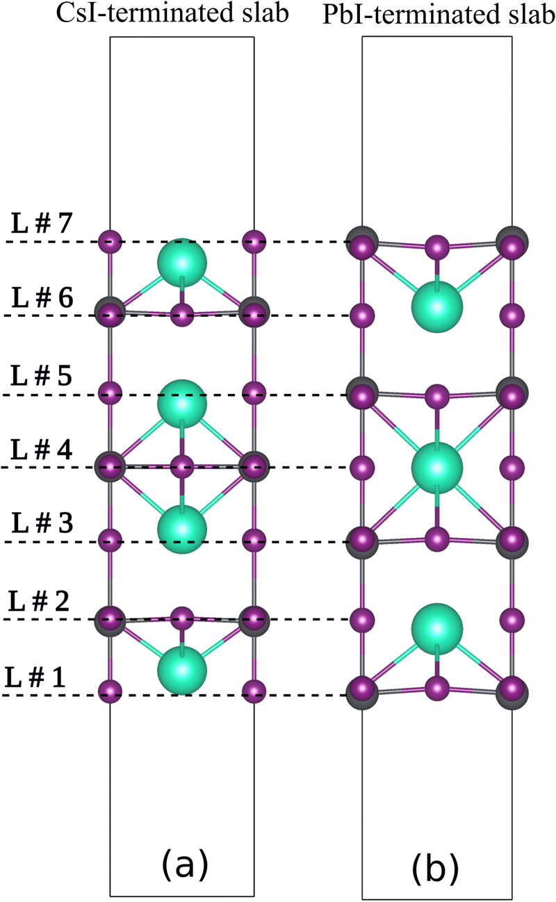
The optimized lattice constant of α-CsPbI3 was driven in this work, which was 6.3877 Å. It was in agreement with the values obtained in an experiment (6.2894 Å) and calculated in another DFT research (6.4011 Å).19,20 After convergence tests over the parameters related to α-CsPbI3 bulk structure, the CsI-terminated, and PbI2 terminated slabs produced in (001) direction with three octahedral layers (seven atomic layers) and 17 Å vacuum between consecutive images to model perovskite surfaces. The electronic properties were calculated by varying vacuum thickness from 14 to 18 Å, and 17 Å was the limit where the properties were almost fixed. The 7 × 7 × 7 and 6 × 6 × 1 Monkhorst–Pack grids are used for bulk and slabs Brillouin-zone (BZ) integration, respectively. The atomic positions are relaxed until the residual forces on each atom become less than 0.001 Ry Bohr−1. After optimizing the bulk and 2D structures, some atoms were moved toward the x and z directions to evaluate the effect of displacement in the splitting of the band structure. The movement of atoms happened in the steps of 0.1 A, and the displacement was fixed when the splitting was observed. This means that this article's reporting value of displacement is the distance in which the band splitting due to the symmetry breaking starts. This order of atom dislocation was also already studied experimentally.21 According to an investigation by Nazari et al.,22 the surface energy of slabs terminated to CsX and PbX2 (X = I, Br, Cl) changes dramatically for increasing octahedral layers from 1 to 3, and the energy variation is negligible for further increase of layers. Regarding the use of Norm-conserving non-relativistic pseudopotential in the latter research, the surface energy was recalculated for different numbers of layers with regard to relativistic pseudopotential. The obtained results showed that the energy would not change significantly for more than 4 layers and resembles the surface energy of a bulk structure. Finally, three layers were considered, regarding the importance of the surface effect. The electron density value of all the isosurface plots is a default value of the VESTA package, which is 0.0036 Å−3.
3 Results and discussions
3.1 Interplay of spin–orbit coupling and band splitting
In the presence of spin–orbit coupling (SOC), the system Hamiltonian at the first approximation can be written as:| |  | (1) |
The last term in the above equation is denoted as ![[script letter H]](https://www.rsc.org/images/entities/char_e142.gif) SO. It is responsible for the SOC effect in which V, p, and σ stand for the lattice potential, the momentum operator, and Pauli matrices respectively. In nonmagnetic systems lacking inversion symmetry, SOC contribution can be expressed in terms of Rashba–Dresselhaus (RD) Hamiltonian.23,24 Although Rashba–Dresselhaus's effects cause different spin polarization in the band energy and different spin textures, they have a similar band dispersion. Indeed, the solution of the Hamiltonian yields band splitting going from high symmetry special k-points to low symmetry ones in such a way that the degenerate spin band splits into two spin-up and spin-down bands and shifts toward opposite directions in k space. In this case, at the close vicinity of valence band maximum (VBM) and conduction band minimum (CBM), the eigenvalues of can be expressed by25
SO. It is responsible for the SOC effect in which V, p, and σ stand for the lattice potential, the momentum operator, and Pauli matrices respectively. In nonmagnetic systems lacking inversion symmetry, SOC contribution can be expressed in terms of Rashba–Dresselhaus (RD) Hamiltonian.23,24 Although Rashba–Dresselhaus's effects cause different spin polarization in the band energy and different spin textures, they have a similar band dispersion. Indeed, the solution of the Hamiltonian yields band splitting going from high symmetry special k-points to low symmetry ones in such a way that the degenerate spin band splits into two spin-up and spin-down bands and shifts toward opposite directions in k space. In this case, at the close vicinity of valence band maximum (VBM) and conduction band minimum (CBM), the eigenvalues of can be expressed by25
| |  | (2) |
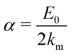
As shown in Fig. 2, km is the displacement of high-symmetry k-point, and α is the band splitting coefficient directly related to the lattice potential gradient. Therefore, it is clear that the intensity of SOC is directly controlled by it. The below relation can calculate these coefficients:25
| |  | (3) |
where
E0 is the energy splitting. The α-CsPbI
3 phase of perovskite has a
Pm![[3 with combining macron]](https://www.rsc.org/images/entities/char_0033_0304.gif) m
m (No. 221) space group with five atoms in the primitive unit cell. As shown in
Fig. 1. Pb, I, and Cs atoms occupy (a), (d), (b) Wyckoff-position and
mm, 4/
mm.
m, and
mm site symmetries, respectively. Slicing the bulk structure in the
z-axis direction ((001) direction) with two possible CsI- and PbI
2 terminations yields two-dimensional slabs with
P4
mm (No. 99) space group. The appearance of heavy atoms such as Pb and I in this material causes the strong SOC effect. Therefore, the inversion asymmetry of the lattice potential gradient can lead to the spin splitting of the degenerate bands.
 |
| | Fig. 1 The structure of bulk CsPbI3 and the atoms go under displacement to create the distortion. As it shows, these atoms move towards two directions of X and Z to axes the effect of distortion on the electronic properties. | |
 |
| | Fig. 2 Spin-up (red) and spin-down (blue) branches are depicted after band splitting. | |
In this article, we explore band splitting in α-CsPbI3 structure based on the analysis of crystal structure. We first investigate the general features of the spin splitting in 3D perovskite. Then, we treat the 2D form of α-CsPbI3 and consider two different terminations, in which bulk lattice and surface structural distortions contribute to the strong band splitting.
3.2 Bulk distortion and SOC-induced band splitting
Due to heavy elements in perovskite materials, the SOC effect has an essential role in the electronic structure of these materials, especially on the band gap. Idrissi and coworkers have shown that the estimated band gap is 1.16 eV using the GGA-PBEsol method, and 0.39 eV while considering SOC correction.26 The calculated energy gap is 0.18 eV in this work, which agrees with Idrissi and other computational results.27,28
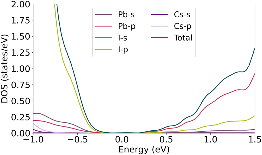
As described in the previous section, symmetry-breaking due to the atoms moving off from their correct Wyckoff positions can cause band splitting of the degenerate spin bands. In this regard, the displacement of α-CsPbI3 atoms is shown in Fig. 1. From the linear combination of atomic orbitals (LCAO) point of view, investigating the projection of valence band states over the atomic orbitals reveals how the orbital contribution changes over distortion. As shown in Fig. 3, the main and slight contributions of orbitals in VBM relate to the p-orbitals of iodine and the s-orbital of lead atoms, respectively. Therefore, the approximate wave function can be expressed as follows
| | | ΨVBM,k ≈ CPbsΦPbs + CI1ΦI1 + CI2ΦI2 + CI3ϕI3 | (4) |
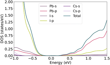 |
| | Fig. 3 Partial density of states of pure bulk CsPbI3. | |
ϕ
Pbs and ϕIi are the lead atomic s-orbital and the iodine atomic p-orbitals, correspondingly. The values of these coefficients determine the strength of orbital overlapping. It is worth mentioning that binding in the xy-plane is accomplished through overlapping between px and py orbitals and s-orbital of iodine (I1, I2) and lead atoms, respectively, while bonding in the z-direction is accomplished through overlapping between pz and s orbitals.
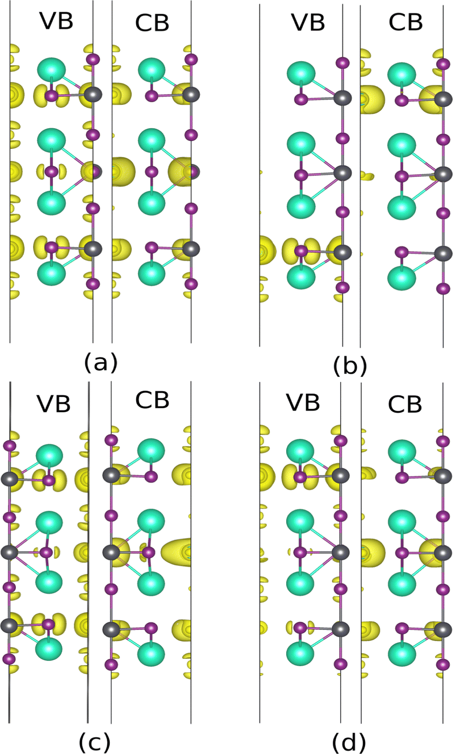
According to the projection of conduction band states over the atomic orbitals, the main contribution of the lead atomic orbitals relates to the p orbitals. In the iodine atom, the half-filled pz orbital contributes more than the filled px and py orbitals in the VB wave function. Regarding the equity of I2, and I3 contributions on the wave function, only I1 and I2 site positions are considered in Table 1. Moving the Cs atom in the x and z directions, equal variations in the band energy are observed due to symmetry correspondences. Since the band splitting may occur in the slight disposition of atoms, 0.1 Å spacial steps are considered for all atoms in the structures. As depicted in Fig. 3, Cs orbitals have no involvement in the edge of VBM and CBM, hence no splitting is observed by moving Cs atom up to 0.5 Å in the x and z axis. The amount of α in the vicinity of CBM and VBM, represented as αc and αv, is negligible, thus the band gap remains almost unchanged at about 0.18 eV. This behavior, however, is not observed for atoms in octahedral cages, involving iodine and lead. As characterized in Fig. 4, the lead s orbital and iodine p-orbital have significant contributions in VBM. Any changes in bond length can affect the strength of the bonding. For instance, moving I2 atom along the z-direction decreases the overlap of iodine pz and lead s orbital, and increases the overlapping of the px and py orbitals of the two other iodine atoms with the lead s orbital.
Table 1 The expansion coeffcient of the wave-function in terms of the atomic orbitals for pure (the crystal without distortion) and the distorted crystal (extracted from the projected density of states)
| Case |
C
Pb
|
C
I1
|
C
I2
|
C
I3
|
| Pure |
0.226 |
0.152 |
0.182 |
0.152 |
| Pb-x |
0.244 |
0.148 |
0.246 |
0.176 |
| Pb-z |
0.242 |
0.194 |
0.198 |
0.194 |
| I1-x |
0.214 |
0.13 |
0.258 |
0.186 |
| I1-z |
0.206 |
0.158 |
0.226 |
0.182 |
| I2-x |
0.218 |
0.184 |
0.232 |
0.186 |
| I2-z |
0.2 |
0.204 |
0.138 |
0.204 |
 |
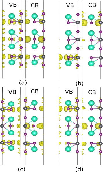
| | Fig. 4 Iso surfaces of VBM and CBM of bulk CsPbI3 (a) with Pb moving in the z or x-direction (b), with I1 moving in x (c) and z (d) directions, and with I2 displaced in x (e) and z (f) direction. | |
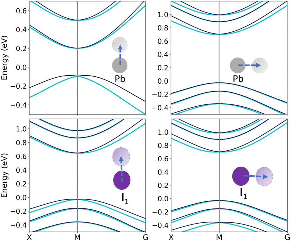
Since Pb orbitals have no significant effect on VBM, 0.2 Å displacement of Pb atom along the x or z direction band splitting is not observed. Expansion of relocation to 0.5 Å results in a detectable splitting on both VBM and CBM, widening the band gap.
Since the p-orbital of the iodine atoms forms almost the dominant contribution of orbitals near VBM, and it has a small but not negligible share on CBM, 0.2 Å displacement of I1 along the x direction would split the band up to 1.67 for αv and 1.23 for αc. Changing the z coordinate of this atom also causes noticeable splitting in the valence band with αv as 0.89 and αc as 0.79. The splitting coefficients and the band gap of the distorted structures are reported in Table 2. Moreover, energy variations are depicted in Tables 2 and 3, where ΔE is the energy difference between the pure and distorted structures. Regarding the results, the highest energy variation in bulk structure is related to Pb distortion, which is about −0.3 eV. Other distortions lead to variations in the orders of 0.01 to 0.001. Another notable point is the sign of energy changes. For whole distortions, except the Cs atom, the energy difference is negative, which means the presence of a distorted Cs atom in the CsPbI3 structure is the most likely. Similarly, the presence of a distorted Pb atom in the structure is the least possible situation (Fig. 5).
Table 2 Changes in the band splitting coefficient as a function of the atomic displacement (d) in the x and z direction for the Valence and conduction bands (VB/CB) and ΔE (the difference energy between pure and distorted) in CsPbI3 bulk structure
| Case |
d (A) |
α
v (V Bohr−1) |
α
c (V Bohr−1) |
E
g (eV) |
ΔE (eV) |
| Cs-x,z |
0.2 |
0 |
0 |
0.18 |
+0.028 |
| Pb-x |
0.5 |
0.25 |
0.42 |
0.71 |
−0.32 |
| Pb-z |
0.5 |
0.14 |
0.24 |
0.71 |
−0.32 |
| I1-x |
0.2 |
1.67 |
1.23 |
0.36 |
−0.035 |
| I1-z |
0.2 |
0.89 |
0.79 |
0.25 |
−9.e-4 |
| I2-x |
0.2 |
0.85 |
1.52 |
0.22 |
−9.e-4 |
| I2-z |
0.2 |
0.94 |
0.31 |
0.40 |
−0.035 |
Table 3 Changes in the band splitting coefficient as a function of the atomic displacement (d) in the x and z direction for the Valence and conduction bands (VB/CB) and ΔE in CsI and PbI2 terminated slabs
| Surface |
Case |
d (A) |
α
v (V Bohr−1) |
α
c (V Bohr−1) |
E
g (eV) |
ΔE (eV) |
| CsI slab |
Pure |
— |
— |
— |
0.66 |
— |
|
|
Pb-x |
0.2 |
0.0 |
0.21 |
0.70 |
−0.045 |
|
|
Pb-z |
0.2 |
0.13 |
0.04 |
0.29 |
−0.061 |
|
|
I1-x |
0.2 |
0.12 |
0.26 |
0.68 |
−0.057 |
|
|
I1-z |
0.2 |
0.24 |
0.16 |
0.67 |
−0.005 |
| PbI2 slab |
Pure |
— |
— |
— |
0.45 |
|
|
|
Cs-x |
0.2 |
0.0 |
0.0 |
0.45 |
+0.003 |
|
|
Cs-z |
0.2 |
0.33 |
0.29 |
0.32 |
−0.004 |
|
|
I2-x |
0.4 |
0.12 |
0.58 |
0.46 |
−0.01 |
|
|
I2-z |
0.2 |
0.14 |
1.26 |
0.09 |
−0.123 |
 |
| | Fig. 5 Band structures of distorted bulk CsPbI3 with changes in Cs, iodine, and Pb coordinates. | |
3.3 Effect of surface-termination on SOC-induced band splitting
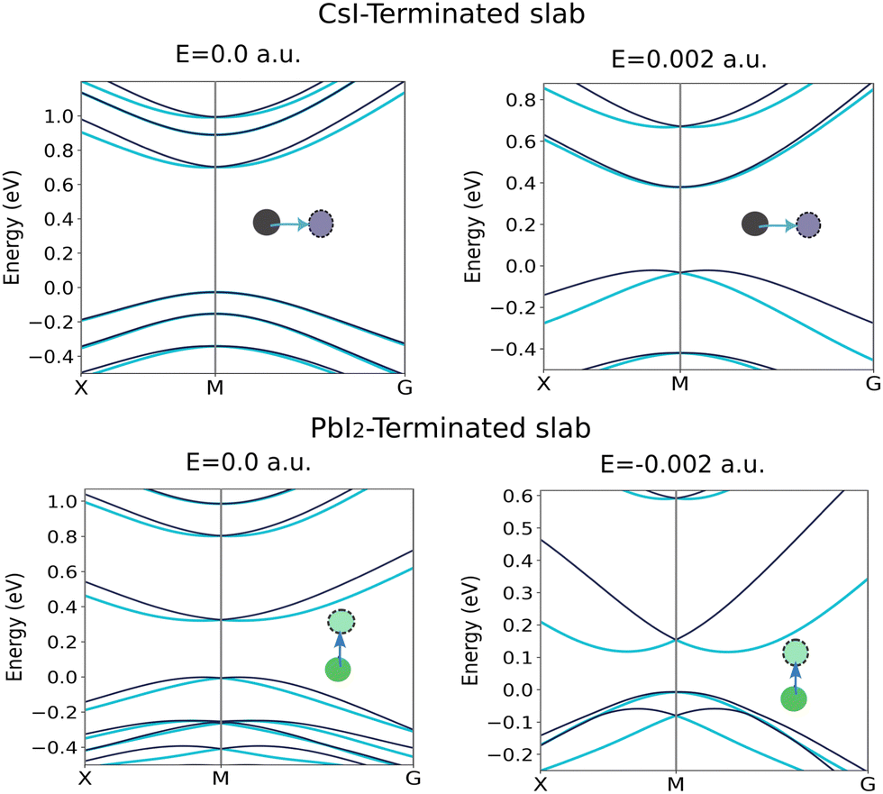
In this section, the effect of the presence of crystal defects as the small distortion on CsPbI3 slabs has been investigated to clarify SOC-induced band splitting in 2D perovskite material. Moreover, the influence of slab termination on spin splitting has been looked over. Two structures with seven layers were considered with different terminations: CsI-termination and PbI2-termination (Fig. 6). The band gaps of two slabs are calculated as 0.66 eV and 0.45 eV for CsI and PbI2-terminated slabs respectively, which are in agreement with Long and coworkers study.29
 |
| | Fig. 6 The side view of CsI-terminated (a) PbI2-terminated (b) films. | |
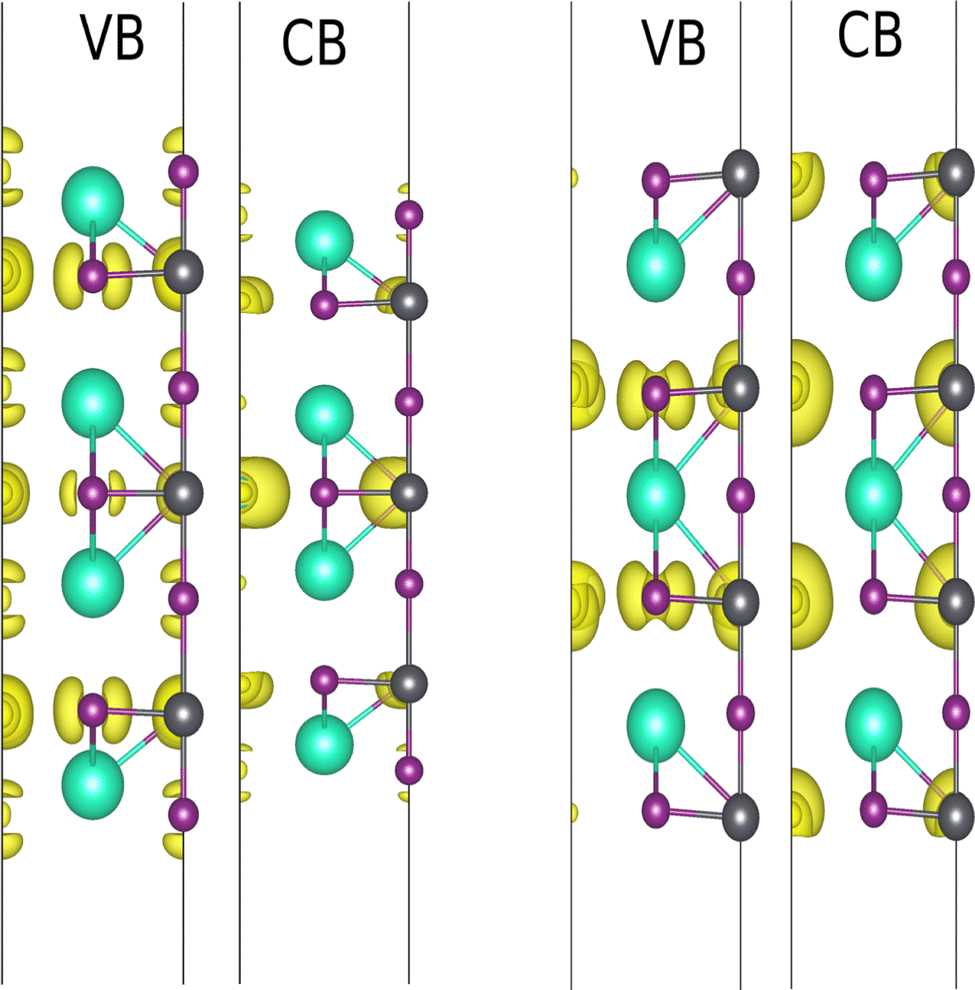
Similar to the previous section, the contributions of the atomic layers on VBM and CBM are characterized before and after defect consideration. In this regard, the iso-surfaces of the 2D structures were calculated, which are shown in Fig. 7. The p orbital of the iodine atoms and the s orbital of the lead atom form the VBM, while CBM is mainly made of the p-orbital. As indicated in Fig. 7, PbI2 atomic layers’ contribution is dominant for both VBM and CBM, while CsI atomic layers can be ignored. It should be noted that the main contribution in CBM for both terminations comes from the internal layers. It also has been shown that the main contribution in VBM of PbI2-termination is due to px and py orbitals of I1 and I3, whereas VBM of CsI-termination comes from the whole p orbitals (Fig. 8).
 |
| | Fig. 7 Iso surface of non-distorted CsI- (a) and PbI2 – (b) terminated slabs. | |
 |
| | Fig. 8 CsI-slab band splitting within displacements of Pb and I1 atoms along the x and z axis. | |
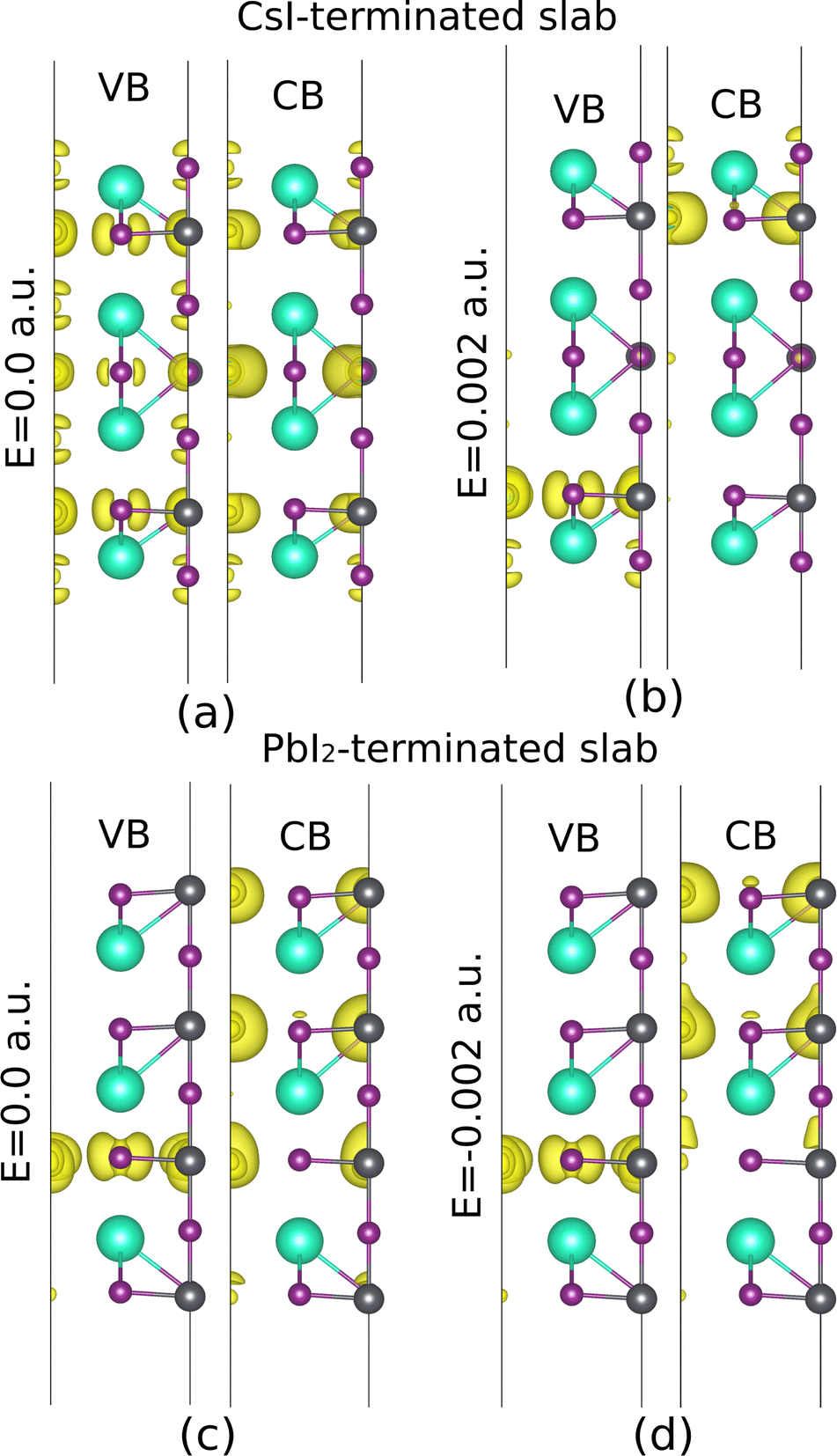
In the next step, the influence of breaking the symmetry was studied using a minor displacement of 0.2 Å in the central layers (L#4). In the CsI-terminated slab, when the Pb atom moves along the z-direction, it gets closer to the iodine atom on the surface including (I2), and further from the iodine in the PbI2 plane. As depicted in Fig. 9(b) the main contribution for VB and CB comes from L#2 and L#6, respectively. In the VB, the s orbital of Pb and Px and Py orbitals of I1 and I3 are dominant, whereas the contribution of pz orbital of I2 has been shrunk. A decrease in the contribution of other orbitals in VBM and non-zero local potential led to a smaller gap of 0.29 eV and an apparent splitting in VB. The main contribution in CB is due to the lead p orbital in L#6, while a small contribution is observed due to pz orbital of I2 in L#7. For moving I2 along the z-direction, similar description can be made. Another considerable point is that displacement of I1 and Pb along the z-direction leads to an opposite behavior in VBM and CBM. Put another way, the mentioned distortion changes the potential gradient vice verse and can be attributed to the opposite polarization direction.
 |
| | Fig. 9 Iso surface near VBM and CBM of CsI-slab without external field with displacement in the x-direction of Pb (a), z-direction of Pb (b), x-direction of I1 (c), z-direction of I1 (d). | |
In the following, the behavior of the PbI2 slab regarding to Cs and I2 displacement along the x- and z-direction is investigated (Fig. 11). As it is known, the splitting coefficient directly relates to the gradient of the local electrostatic potential, which is determined by structural distortion. The near-zero splitting indicates that the potential gradient's value is insignificant. Moving the Cs atom along the x direction, the behavior of the terminated PbI2 slab is almost the same as the non-distorted structure. Therefore the band splitting is zero. But, the situation is entirely different when Cs move along the z-direction. In the latter case, contrary to the bulk structure, the band splitting is detectable in VBM and CBM. Although the energy band related to the Cs atom doesn't contribute to VBM or CBM, a slight displacement of this atom along the z-direction can lead to convert a direct gap into an indirect energy gap, as shown in Fig. 10. In this case, similar to f the CsI-terminated slab, the behavior of Cs and I2 are almost entirely inverse to each other.
 |
| | Fig. 10 PbI2-slab band splitting within displacements of Cs and I2 atoms along the x and z axis. | |
 |
| | Fig. 11 Iso surfaces near VBM and CBM of PbI2-slab without external field with displacement in the x-direction of Cs (a), z-direction of Cs (b), x-direction of I2 (c), z-direction of I2 (d). | |
Regarding Cs displacement in the z direction, the main contribution in VB ascribed to px and py orbitals and the s atomic orbital of lead located in L#3, while it comes from L#5 with the same orbitals about I2. There, however, is a considerable difference between the spin splitting in I2 concerning Cs in CBM, as depicted in Fig. 11. To gain better insight, the projection of valence band states over the atomic orbitals was investigated, and the main contribution of atomic orbitals was compared in CB. According to the obtained data after displacing Cs and I2 in the z-direction, the approximate wave functions can be written in eqn (5) and (6), respectively.
| ΨCBMkCs ≈ 2 × 0.163PbpΦL#5 + 2 × 0.098PbpΦL#7 |
| | | +2 × 0.092PbpΦL#3 + 2 × 0.032PbpϕL#1 | (5) |
| |  | (6) |
where
kCs and
kI2 are (0.5, 0.4875, 0.0) and (0.475, 0.475, 0.0), respectively. As described in the previous sections, CBM is formed from the p orbitals of lead and a slight contribution of the p orbital of iodine atoms.
3.4 External field
So far, we explained symmetry breaking originated from atomic displacements—. The results indicated that the band splitting does not follow an identical behavior, rather it depends on the site symmetry of the displaced atoms. The question addressed in the last part of this research is how to control the band splitting using an exterior factor, namely, an external electric field. In a realistic system structural symmetry breaking, such as point defect, occurs normally. Therefore the control of band structure properties as an important tool for characterizing electronic and spintronic structure can be very important. Depending on the polarization direction in CBM or VBM, we examined different values of the external electric field to control the spin splitting. The calculated coefficients of the band splitting are given in Table 4. Based on the obtained results, there is a threshold electric field in which band-splitting behavior will almost be reversed.
Table 4 Effect of an external field on band splitting near VBM and CBM of two surfaces as CsI and PbI2-terminated slabs
| Surface |
Case |
d (A) |
![[scr E, script letter E]](https://www.rsc.org/images/entities/char_e140.gif) (a.u.) (a.u.) |
α
v (V Bohr−1) |
α
c (V Bohr−1) |
E
g (eV) |
| CsI slab |
Pb-x |
0.2 |
0.002 |
0.52 |
0.08 |
0.40 |
|
|
Pb-z |
0.2 |
−0.002 |
0.24 |
0.04 |
0.08 |
|
|
I1-x |
0.2 |
0.0025 |
0.58 |
0.08 |
0.29 |
|
|
I1-z |
0.2 |
0.0022 |
0.59 |
0.04 |
0.29 |
| PbI2 slab |
Cs-x |
0.2 |
0.0 |
0.0 |
0.0 |
0.45 |
|
|
Cs-z |
0.2 |
−0.002 |
0.05 |
0.91 |
0.32 |
|
|
I2-x |
0.4 |
0.001 |
0.23 |
0.69 |
0.39 |
|
|
I2-z |
0.2 |
0.0001 |
0.16 |
1.22 |
0.07 |
Our studies on this subject show that we can increase or decrease the splitting coefficients or even eliminate them in some cases by an external electric field.
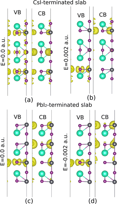
A Pb atom located in L![[triple bond, length as m-dash]](https://www.rsc.org/images/entities/char_e002.gif) 4 of the CsI-terminated slab has been displaced along the positive x-direction and, meanwhile, has been exposed to an external electric field in the positive z-direction. The splitting in CBM closes, whereas VBM starts to open, and this behavior follows up till the electric field amount reaches 0.002 a.u., as shown in Fig. 12 and 13(b). The discussion about the Cs atom located in L#4 of the PbI2-terminated slab and displaced along the positive z-direction is completely different. When this atom is exposed to an electric field in the negative z-direction, a vice versa conclusion is observed (Fig. 12 and 13(d)) considering the electric fields in these two cases are opposite, this can be a clue showing anti-parallel polarization between the two examined slabs.
4 of the CsI-terminated slab has been displaced along the positive x-direction and, meanwhile, has been exposed to an external electric field in the positive z-direction. The splitting in CBM closes, whereas VBM starts to open, and this behavior follows up till the electric field amount reaches 0.002 a.u., as shown in Fig. 12 and 13(b). The discussion about the Cs atom located in L#4 of the PbI2-terminated slab and displaced along the positive z-direction is completely different. When this atom is exposed to an electric field in the negative z-direction, a vice versa conclusion is observed (Fig. 12 and 13(d)) considering the electric fields in these two cases are opposite, this can be a clue showing anti-parallel polarization between the two examined slabs.
 |
| | Fig. 12 The spin band splitting of the CsI and PbI2-terminated slab with and without field. | |
 |
| | Fig. 13 The averaged induced charge density of the CsI and PbI2-terminated slabs, with a displacement of I2 along the x-direction in CsI-terminated slab, and Cs along the z-direction in PbI2. The electric field is not considered in (a) and (c), while it has been applied in (b) and (d). | |
4 Conclusion
This study was designed to characterize the electronic structure and spin properties of bulk and two terminations of the CsPbI3 perovskite slabs in (001) direction in the presence of geometrical distortions. A tight correlation among the SOC-induced band splitting of VB/CB, site symmetry, and the type of slab termination was recognized. The main idea of this work is to apply the external field as a factor for controlling polarization and subsequently band splitting due to the atomic displacement in different site symmetries. Our findings show that, generally, band splitting can be compensated by a threshold electric field. In other words, the electric field is a deterministic factor in controlling the band splitting, thus increasing or decreasing the recombination rate.
Conflicts of interest
There are no conflicts to declare.
References
- C. R. Kagan, D. B. Mitzi and C. D. Dimitrakopoulos, Science, 1999, 286, 945–947 CrossRef CAS PubMed.
- G. Lin, Y. Lin, R. Cui, H. Huang, X. Guo, C. Li, J. Dong, X. Guo and B. Sun, J. Mater. Chem. C, 2015, 3, 10793–10798 RSC.
- A. Kojima, K. Teshima, Y. Shirai and T. Miyasaka, J. Am. Chem. Soc., 2009, 131, 6050–6051 CrossRef CAS PubMed.
- S. D. Stranks, G. E. Eperon, G. Grancini, C. Menelaou, M. J. Alcocer, T. Leijtens, L. M. Herz, A. Petrozza and H. J. Snaith, Science, 2013, 342, 341–344 CrossRef CAS PubMed.
- G. Xing, N. Mathews, S. Sun, S. S. Lim, Y. M. Lam, M. Grätzel, S. Mhaisalkar and T. C. Sum, Science, 2013, 342, 344–347 CrossRef CAS PubMed.
- W. Zhang, G. E. Eperon and H. J. Snaith, Nat. Energy, 2016, 1, 1–8 Search PubMed.
- G. Schileo and G. Grancini, J. Phys. Energy, 2020, 2, 021005 CrossRef CAS.
- Q. A. Akkerman, M. Gandini, F. Di Stasio, P. Rastogi, F. Palazon, G. Bertoni, J. M. Ball, M. Prato, A. Petrozza and L. Manna, Nat. Energy, 2016, 2, 1–7 Search PubMed.
- D. Bai, H. Bian, Z. Jin, H. Wang, L. Meng, Q. Wang and S. F. Liu, Nano Energy, 2018, 52, 408–415 CrossRef CAS.
- Y. Wang, T. Zhang, M. Kan, Y. Li, T. Wang and Y. Zhao, Joule, 2018, 2, 2065–2075 CrossRef CAS.
- J. Zhang, D. Bai, Z. Jin, H. Bian, K. Wang, J. Sun, Q. Wang and S. Liu, Adv. Energy Mater., 2018, 8, 1703246 CrossRef.
- F. IS, M. K. Mohanta and A. D. Sarkar, J. Phys.: Condens. Matter, 2023, 35, 253001 CrossRef CAS PubMed.
- C. Katan, L. Pedesseau, M. Kepenekian, A. Rolland and J. Even, J. Mater. Chem. A, 2015, 3, 9232–9240 RSC.
- J. Xue, Y. Huang, Y. Liu, Z. Chen, H. H.-Y. Sung, I. D. Williams, Z. Zhu, L. Mao, X. Chen and H. Lu, Angew. Chem., Int. Ed., 2023, 62, e202304486 CrossRef CAS PubMed.
- G. Huang, S. Rassel, J. Qu, S. Xu, C. Wang and D. Ban, J. Appl. Electron. Mater., 2021, 3, 285–291 CrossRef CAS.
- P. Giannozzi, S. Baroni, N. Bonini, M. Calandra, R. Car, C. Cavazzoni, D. Ceresoli, G. L. Chiarotti, M. Cococcioni, I. Dabo, A. D. Corso, S. de Gironcoli, S. Fabris, G. Fratesi, R. Gebauer, U. Gerstmann, C. Gougoussis, A. Kokalj, M. Lazzeri, L. Martin-Samos, N. Marzari, F. Mauri, R. Mazzarello, S. Paolini, A. Pasquarello, L. Paulatto, C. Sbraccia, S. Scandolo, G. Sclauzero, A. P. Seitsonen, A. Smogunov, P. Umari and R. M. Wentzcovitch, J. Phys.: Condens. Matter, 2009, 21, 395502 CrossRef PubMed.
- D. M. Ceperley and B. Alder, Phys. Rev. Lett., 1980, 45, 566 CrossRef CAS.
- J. P. Perdew and A. Zunger, Phys. Rev. B: Condens. Matter Mater. Phys., 1981, 23, 5048 CrossRef CAS.
- D. Trots and S. Myagkota, J. Phys. Chem. Solids, 2008, 69, 2520–2526 CrossRef CAS.
- M. Afsari, A. Boochani and M. Hantezadeh, Optik, 2016, 127, 11433–11443 CrossRef CAS.
- H. Hashimoto, M. Kuwabara, Y. Takai, S. Tsubokawa and Y. Yokota, J. Electron Microsc. Tech., 1989, 12, 180–200 CrossRef CAS PubMed.
- S. Nazari, Y. T. Azar and A. Doroudi, Mater. Today Commun., 2020, 24, 100961 CrossRef CAS.
- E. Rashba, Sov. Phys. Solid State, 1960, 2, 1109 Search PubMed.
- G. Dresselhaus, Phys. Rev., 1955, 100, 580 CrossRef CAS.
- M. Kepenekian, R. Robles, C. Katan, D. Sapori, L. Pedesseau and J. Even, ACS Nano, 2015, 9, 11557–11567 CrossRef CAS PubMed.
- S. Idrissi, H. Labrim, L. Bahmad and A. Benyoussef, Chem. Phys. Lett., 2021, 766, 138347 CrossRef CAS.
- L.-K. Gao and Y.-L. Tang, ACS Omega, 2021, 6, 11545–11555 CrossRef CAS PubMed.
- M. Afsari, A. Boochani, M. Hantezadeh and S. M. Elahi, Solid State Commun., 2017, 259, 10–15 CrossRef CAS.
- L. Long, D. Cao, J. Fei, J. Wang, Y. Zhou, Z. Jiang, Z. Jiao and H. Shu, Chem. Phys. Lett., 2019, 734, 136719 CrossRef CAS.
|
| This journal is © the Owner Societies 2024 |
Click here to see how this site uses Cookies. View our privacy policy here. 
 *a,
Fatemeh Mohammad
Dezashibi
b and
Nadia Babaei
Bidmeshki
a
*a,
Fatemeh Mohammad
Dezashibi
b and
Nadia Babaei
Bidmeshki
a