Flexible piezo-resistive strain sensors using all-polydimethylsiloxane based hybrid nanocomposites for wearable electronics
Received
29th August 2023
, Accepted 21st November 2023
First published on 22nd November 2023
Abstract
We report flexible piezo-resistive strain sensors composed of silver nanoparticle (Ag NP), graphene nanoplatelet (GNP), and multi walled carbon nanotube (MWCNT)-based ternary conductive hybrid nanocomposites as an active sensing layer fabricated using a simple solution processing method on flexible polydimethylsiloxane (PDMS) substrates. The electrical characteristics have been studied in PDMS-based flexible devices having three different kinds of structures, namely Ag NPs/MWCNT/PDMS, GNP/PDMS and Ag NPs/GNP/PDMS. The microscopic analysis of the hybrid nanocomposites is undertaken using field emission scanning electron microscopy. The diameter of the CNTs is found to be in the range of 20–40 nm, whereas the length is determined to be 100–800 nm. The average diameter and length of the GNPs are observed to be 30–50 nm and 100–500 nm, respectively. The crystallite size of the silver nanoparticles in the Ag NPs/MWCNT/PDMS and Ag NPs/GNP/PDMS-based nanocomposites is determined to be 22.8 nm and 29.1 nm, respectively. The prepared sample of Ag NPs shows four distinct peaks in the X-ray diffraction pattern, which correspond to the (111), (200), (220), and (311) face-centered cubic (FCC) crystalline planes. Raman spectroscopy is undertaken to study the fundamental physical properties and chemical analysis of the nanocomposites. Ag NPs/GNP/PDMS-based sensors exhibit superior performance in terms of sensitivity, response and recovery time during breathing/unbreathing analysis. The large surface area of the Ag NPs and GNPs promotes uniform distribution of Ag NPs to fill into the porous GNP surface, thereby facilitating high contact area along with better electron transport in the Ag NPs/GNP/PDMS hybrid nanocomposite-based sensors. The gauge factor (GF), response and recovery time of the Ag NPs/GNP/PDMS hybrid nanocomposite-based sensors are determined to be 221, 130 ms and 119 ms, respectively. The ternary conductive nanocomposite-based sensors are free from the drawbacks of binary nanocomposite-based sensors where the high percolation threshold and poor mechanical behaviour lead to the degradation of the device performance.
1 Introduction
Currently, modern technology is experiencing substantial growth in the area of flexible and wearable electronics. Wearable strain sensors, in particular, have gained keen interest for their capability of sensing mechanical deformation and thereby playing a pivotal role for application in biomedical devices, E-skin, robotics, strain gauge, aircraft, microfluidics and health monitoring devices.1–4 However, flexible sensors mounted on the human body are capable of detecting not only high pressure but also low pressure and strain. Moreover, flexible and wearable sensors can be attached on the human body to monitor blood pressure, heart rate and body temperature by bending and movement of fingers and body parts.2 Furthermore, these sensors can be used for human health monitoring,3 human motion detection4,5 and soft robotics applications.6,7 There are four major sensing techniques used in strain sensors, such as capacitive sensing,8,9 piezo-electric sensing,10 piezo-resistive sensing11–13 and optical sensing.14,15 Reports are also available in the literature on flexible pressure, strain sensors and carbonaceous nanomaterials for application in motion monitoring, electronic skin, solid-state supercapacitors, speech/handwriting recognition, etc.16–20 Generally, strain sensors consist of an electrically sensing material deposited on a specific substrate. These sensors detect strain by measuring the variations in resistance,11–13 capacitance,6–9 inductance21 or electric charge. Strain refers to the change in length by twisting, compression and expansion.22,23 The sensitivity of these sensors is evaluated by determining the GF. The basic principle behind piezoresistive pressure sensors is the piezoresistive effect, i.e. the change in electrical resistance of a material with applied mechanical stress or strain. The piezoresistive effect is typically quantified using a dimensionless parameter called the GF. GF is defined as the ratio of the fractional change in resistance to the applied strain. Piezoresistive pressure sensors consist of a thin flexible material that deflects under the influence of an applied pressure. When pressure is applied to the flexible system, it deforms, facilitating the sensor to experience mechanical stress. This stress leads to a change in the electrical resistance of the sensor, which is proportional to the applied pressure.24 PDMS, silly putty, glass fiber, polyethylene terephthalate (PET), PMMA, nitrile rubber and PEDOT:PSS have been used as flexible substrates for the fabrication of strain sensors along with a thin sensing layer.22 PDMS is a silicone based elastomeric polymer having some unique properties for biomedical applications, such as physiological indifference, excellent resistance to biodegradation, biocompatibility, chemical stability, gas permeability, good mechanical properties, excellent optical transparency and ease of device processing.25 Moreover, PDMS is considered to be the most promising elastomer compared to glass and silicon, since the latter materials have a high manufacturing cost, high labour intensity and rigid nature. Furthermore, the variable elasticity of PDMS (modulus of elasticity is 1–3 MPa compared to ∼50 GPa of glass) is suitable for biomedical applications.26,27 In addition, PDMS is thermally stable, is easy to handle, represents isotropic and homogeneous behaviour, develops submicron features for microstructures28–30 and is suitable for thermal and electrical insulation.31 It may be mentioned here that PDMS shows a hyperelastic behaviour, i.e. the ability of a material to undergo large deformations before rupture.32 Similar characteristics are also found in biological tissues and, thus, PDMS is a well-suited material for wearable electronics such as E-skin, and tactile sensing applications. Therefore, PDMS has been employed as a substrate for the development of flexible sensors.
It is worth mentioning that electrical conductivity can be increased by several orders of magnitude by adding different nanofillers, viz. MWCNT, GNP, and Ag NPs into flexible polymer matrices.33,34 The inherent resistance of nanofillers, the resistance between nearby NPs and electron tunnelling between NPs have a significant impact on the electrical characteristics of hybrid nanocomposites.35 Conductive materials such as carbon nanotubes,36–38 graphene,39–45 carbon black,46 graphene nanoplatelets,47–49 and reduced graphene oxide50 are frequently added into PDMS to improve the electrical conductivity of strain sensors as well as other electronic devices. Therefore, hybrid nanocomposites have emerged as a possible alternative due to their unique characteristics, such as super-high electrical conductivity, mechanical strength, and biocompatibility. Though nanocomposite thin films for the fabrication of flexible strain sensors are found to be promising, it still poses a problem to developing sensors having high sensitivity, long-term stability, repeatability, durability and wide measurement range. Real-time monitoring of vital signals of patients is possible by hybrid nanocomposite-based sensors. Reports are available in the literature where most of the conductive nanocomposites are based on binary composites. Though simple and low-cost preparation processes of binary nanocomposites lead to superior electrical conductivity, they facilitate high percolation threshold and poor mechanical behaviour. So, it is pertinent to develop ternary nanocomposites in order to further inhibit the percolation threshold of the composites by incorporating a nanofiller through the synergy of hybrid fillers.51
In this work, we thus report the fabrication and characterisation of different conductive hybrid nanocomposite-based sensors with structures Ag NPs/MWCNT/PDMS, GNP/PDMS and Ag NPs/GNP/PDMS with an aim to study their efficacy as flexible strain sensors.
2 Experimental
2.1 Material synthesis and preparation
2.1.1 Preparation of a flexible PDMS substrate.
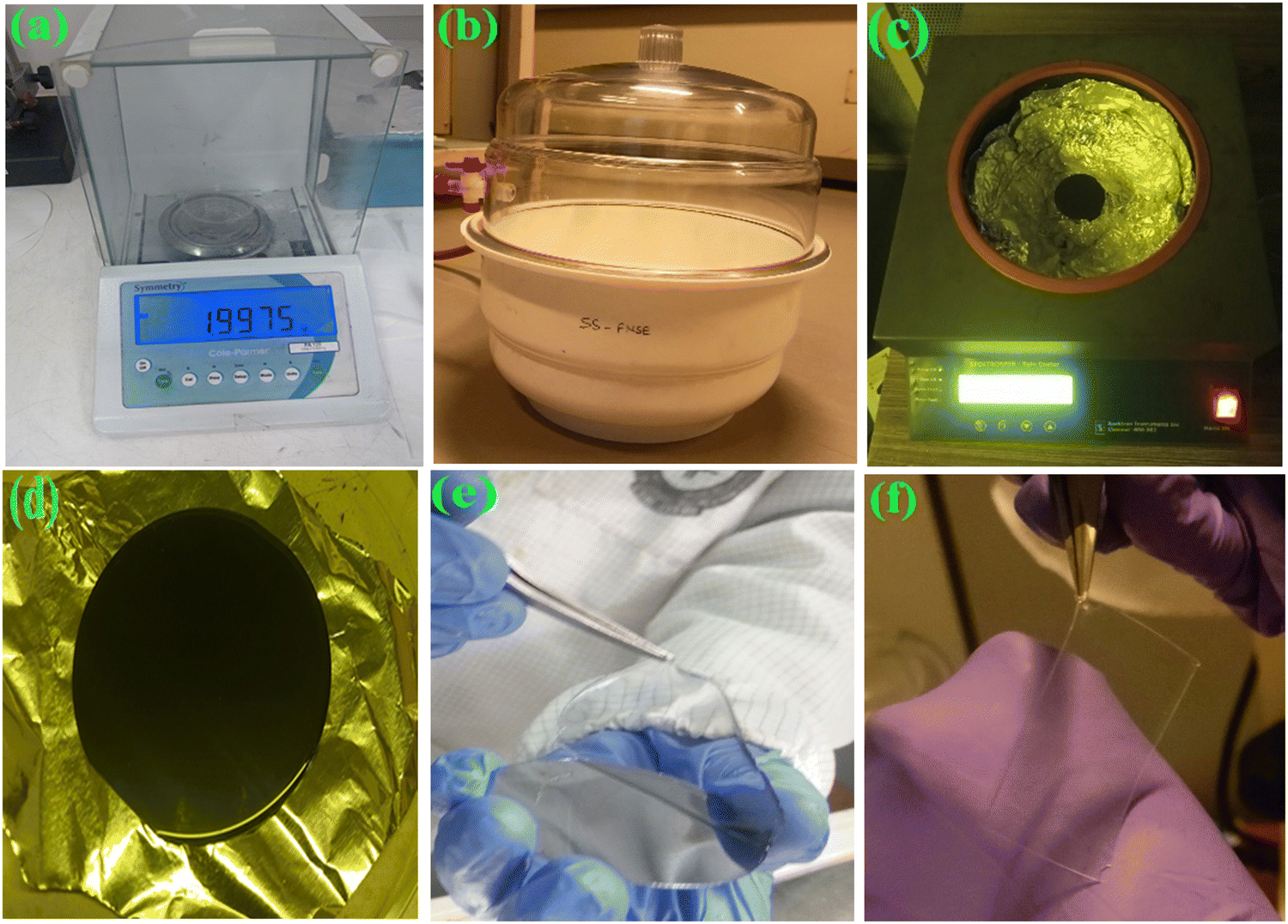
To prepare a PDMS substrate, a silicone elastomer kit (SYLGARD™ 184) was purchased from Dow Corning. It also acts as a transparent encapsulant with good flame-retardant properties. Base and curing agent of silicon elastomer were mixed in a ratio of 10![[thin space (1/6-em)]](https://www.rsc.org/images/entities/char_2009.gif) :1. A vacuum desiccator is used to remove the air bubbles from the mixture. The mixture is deposited on a circular silicon wafer using a spin coater at a spin speed of 350 rpm. The mixture is then subjected to baking at 80 °C for 45 min. Finally, the circular-shaped PDMS substrate is diced into rectangular pieces (Fig. 1).
:1. A vacuum desiccator is used to remove the air bubbles from the mixture. The mixture is deposited on a circular silicon wafer using a spin coater at a spin speed of 350 rpm. The mixture is then subjected to baking at 80 °C for 45 min. Finally, the circular-shaped PDMS substrate is diced into rectangular pieces (Fig. 1).
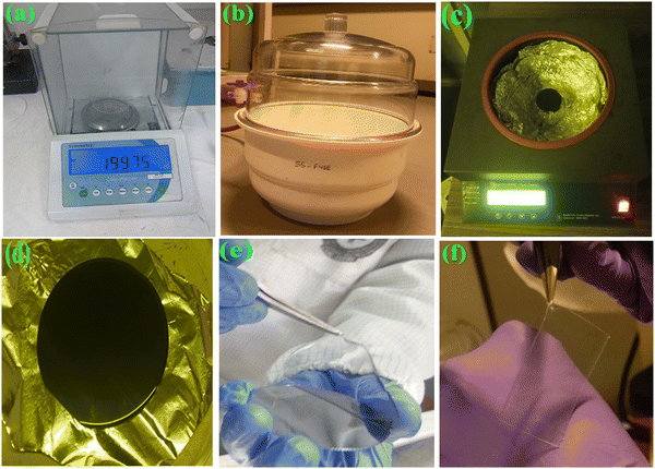 |
| | Fig. 1 Optical images of the fabrication steps during the preparation of flexible PDMS substrates. (a) Measurement of the elastomer and curing agent in the stoichiometric ratio of 10:1 in a weighing machine; (b) a vacuum desiccator containing the mixture of elastomer and curing agent in a beaker to remove air bubbles; (c) the mixture is spin coated on a circular silicon wafer; (d) the mixture is subjected to baking in a closed oven at 80 °C for 45 min; (e) peeling off the PDMS substrate from the silicon wafer and (f) rectangular-shaped PDMS substrates. | |
2.1.2 Synthesis of the Ag NPs/MWCNT/PDMS hybrid nanocomposite.
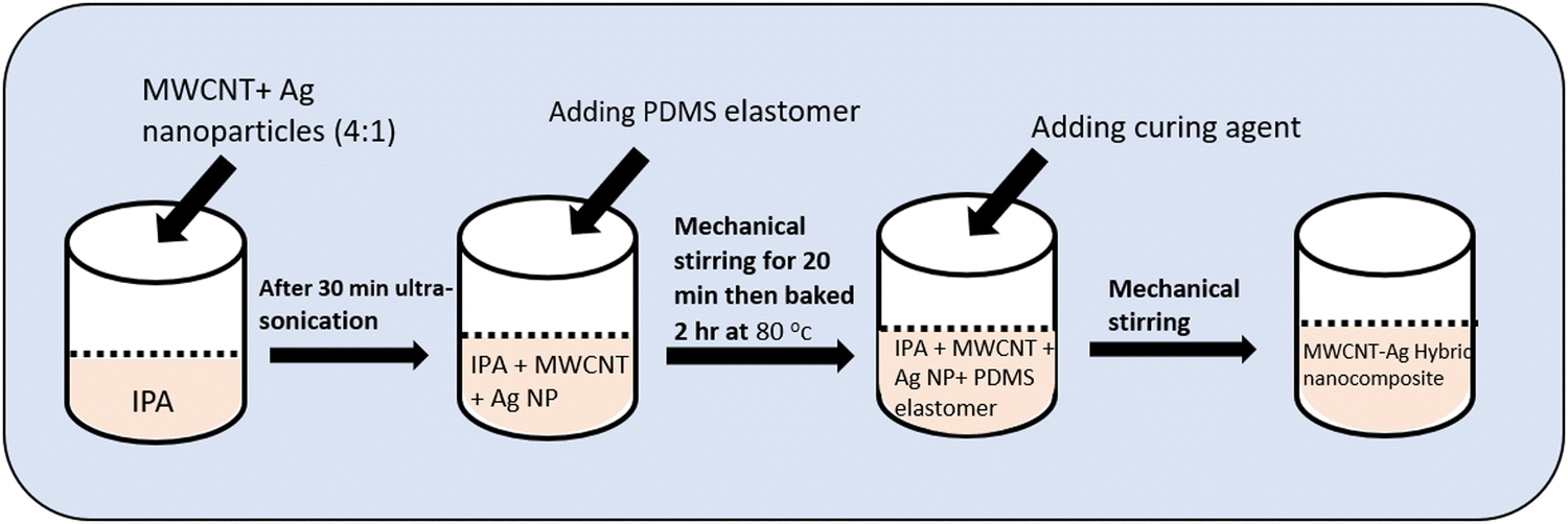
The MWCNT and silver nanoparticles (4:1) are first combined with the requisite amount of isopropyl alcohol. The solution is thereafter ultrasonically sonicated for 30 min to achieve a well-uniform dispersion. The ultrasonic-assisted dispersion is then mixed with 1 g of PDMS elastomer. After that the mixture is manually stirred for 20 min to completely incorporate the Ag NPs/MWCNT nanofillers with the PDMS. The mixture is baked for 2 h at 80 °C to completely evaporate the isopropyl alcohol. The curing ingredient is now added in a 10:1 ratio and mechanically stirred to produce a homogeneous hybrid mixture. A schematic of the processing steps for the preparation of the Ag NPs/MWCNT/PDMS hybrid nanocomposite is shown in Fig. 2.
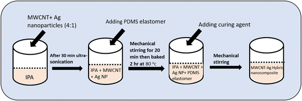 |
| | Fig. 2 Schematic of the processing steps for the preparation of the Ag NPs/MWCNT/PDMS hybrid nanocomposite. | |
2.1.3 Synthesis of the GNP/PDMS hybrid nanocomposite.
Sylgard elastomer and curing agent are taken in the ratio of 10:1. After that, it is mixed inside a glass beaker with 40% graphene of the total solution. To get a uniform mixture it is then subjected to mixing accordingly. To remove the air bubbles, it is finally degassed using a vacuum desiccator.
2.1.4 Synthesis of the Ag NPs/GNP/PDMS hybrid nanocomposite.
Initially, a stoichiometric amount of isopropyl alcohol is taken to make a solution (4:1) of graphene nanoplatelets and silver nanoparticles. To achieve a well-uniform dispersion, the solution is then sonicated using an ultrasonicator for 30 min. Then, 1 g of PDMS elastomer is added to the solution. The mixture is then subjected to stirring mechanically for 20 min to thoroughly mix the nanofillers with PDMS. To evaporate the isopropyl alcohol, the mixture is baked at 80 °C for 2 h. To create a homogenous hybrid mixture, the curing agent is then added in the ratio of 10:1.
2.2 Fabrication of the pressure sensor
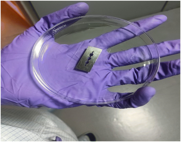
A metal mask is used to transfer the patterned hybrid nanocomposite on a flexible PDMS substrate, as shown in Fig. 3. To fabricate the strain sensor, a hybrid nanocomposite is poured onto the masked PDMS substrate. The mixture is then allowed to spread for a few min. Thereafter, it is subjected to spreading uniformly onto the PDMS substrate using a glass slide manually. The sample is baked at 90 °C for 90 min. A metal contact is formed using silver paste, which is attached to copper wire for further electrical connection.
 |
| | Fig. 3 Optical image of a metal mask on PDMS substrates. | |
2.3 Characterization
Raman experiments were performed at ambient room temperature using the Horiba Scientific Raman system. The microscopic characterizations were undertaken using a field emission scanning electron microscope (Thermoscientific Apreo 2 S) at an accelerating voltage of 10 kV and resolution of 10 μm. Crystal structures of the nanocomposites were obtained by Cu-Kα radiation using an X-ray diffractometer (Rigaku Miniflex II) operated at 30 kV and 15 mA. The electrical performance of the device along with its resistance change were measured by a source meter (Keysight B2901A) and a manual translation stage.
3 Results and discussion
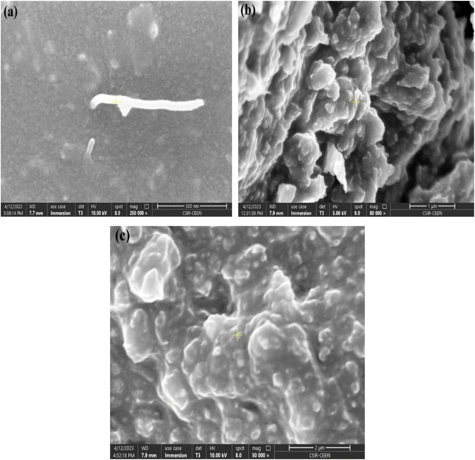
The microstructure of the Ag, GNP, MWCNT and PDMS is observed from the field emission scanning electron microscope (FESEM) images, as shown in Fig. 4. An FESEM image of MWCNT embedded Ag NPs is shown in Fig. 4(a). CNTs along with Ag nanoparticles are observed.
 |
| | Fig. 4 Field emission scanning electron microscopy image of different nanocomposites (a) Ag NPs/MWCNT/PDMS, (b) GNP/PDMS and (c) Ag NPs/GNP/PDMS. | |
The diameter of the tubes is found to be in the range of 20–40 nm, whereas the length is determined to be 100–800 nm. Fig. 4(b) shows the surface morphology of the GNPs deposited on the PDMS substrate suggesting uniform distribution of the GNP particles as well as good adhesion between the GNPs and PDMS matrix. The average diameter and length of the nanoplatelets are found to be 30–50 nm and 100–500 nm, respectively. Fig. 4(c) represents the FESEM image of the Ag-GNP nanoparticles, where silver nanoparticles are distributed on the surface of the graphene nanoplatelets. The XRD technique is used to investigate the crystallographic information, phase purity, crystallite size, and phase constitution of the material.52–59 XRD spectra of the nanocomposites in the 2θ range from 20 to 80° are shown in Fig. 5. For Ag NPs/MWCNT/PDMS and Ag NPs/GNP/PDMS nanocomposites, diffraction peaks of Ag NPs were located at at ∼38.1°, 44.38°, 64.4°, and 77.5°, assigned to the (1 1 1), (2 0 0), (2 2 0) and (3 1 1) face-centered cubic (FCC) crystalline planes, respectively (JCPDS card no. 00-001-1167), as shown in Fig. 5(a) and (c). In the XRD analysis, the diffraction peak at 26.5°, representing (002) facets, corresponds to C NPs for all the nanocomposites, as shown in Fig. 5(a)–(c) (JCPDS card no. 00-056-0159).
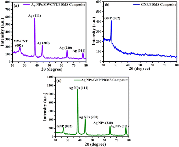 |
| | Fig. 5 XRD pattern of (a) Ag NPs/MWCNT/PDMS, (b) GNP/PDMS and (c) Ag NPs/GNP/PDMS nanocomposites. | |
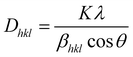
Crystallite size is determined using the Scherrer equation, which can be expressed by eqn (1) below.60
| |  | (1) |
where
Dhkl is the crystallite size in the direction perpendicular to the lattice planes, (
hkl) are the Miller indices of the planes being analysed,
K is a numerical factor frequently referred to as the crystallite-shape factor (0.9),
λ is the wavelength of the X-rays (0.154 nm),
βhkl is the width (full-width at half-maximum) of the X-ray diffraction peak in radians and
θ (2
θ/2) is the Bragg angle corresponding to (
hkl) reflection. The crystallite size obtained from Scherrer and Williamson–Hall models are represented in
Table 1.
Table 1 Comparison of crystallite size of different nanocomposites
| Nanocomposites |
Particles |
Crystallite size (nm) |
| Debye–Scherrer |
Williamson–Hall |
| Ag NPs/MWCNT/PDMS |
C |
5.7 |
3.19 |
|
|
Ag |
22.8 |
19.1 |
| GNP/PDMS |
C |
26.5 |
15.2 |
| Ag NPs/GNP/PDMS |
C |
35.9 |
15.2 |
|
|
Ag |
29.1 |
16.6 |
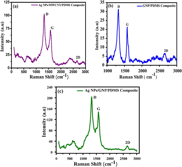
Raman spectroscopy is undertaken to study the fundamental physical properties and chemical analysis of different nanocomposites such as Ag NP/MWCNT/PDMS, GNP/PDMS and Ag NP/GNP/PDMS, as shown in Fig. 6. The bands that appeared at 463.29, 495, 633.03, 796.13 and 855.59 cm−1 are attributed to the existence of Ag NPs in the composite, as shown in Fig. 6(a). Raman spectra at around 1326.53, 1573.64 and 2645.8 cm−1 signify D, G and 2D peaks of MWCNTs, respectively.47Fig. 6(b) representing Raman peaks at 1327.97, 1578 and 2669.12 cm−1 indicates D, G and 2D peaks of GNPs, respectively, in the GNP/PDMS nanocomposite. The D peak signifies the existence of defect states in graphene. The G peak, viz. the characteristic main peak of graphene, is found due to in-plane vibration of sp2 hybridized carbon atoms. The 2D peak, i.e. the two-phonon Raman peak, determines the stacks of carbon atoms present in graphene. Peaks located at 467, 495, 630, 803 and 854 cm−1 are due to the presence of Ag NPs, as shown in Fig. 6(c). The bands that appear at 1338.90, 1567.56 and 2670.91 cm−1 denote the D, G and 2D peaks of GNPs, respectively.
 |
| | Fig. 6 Raman spectra of different nanocomposites: (a) Ag NPs/MWCNT/PDMS, (b) GNP/PDMS and (c) Ag NPs/GNP/PDMS. | |
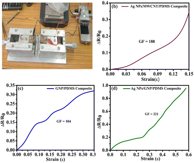
Optical image of the experimental set-up for applying tensile and compressive strain in the device is shown in Fig. 7(a). Fig. 7(b)–(d) show the normalized resistance change with applied strain for different nanocomposite-based strain sensors. At a relatively small strain range of 0–15%, the strain sensor containing the Ag NPs/MWCNT/PDMS nanocomposite has a GF of 188, as shown in Fig. 7(b). From Fig. 7(c), the strain sensor based on GNP/PDMS results in a GF of 104 at strains ranging from 0–30%. The GF of the fabricated strain sensor using Ag NPs/GNP/PDMS is determined to be 221 at the strain ranging from 0–55%. From the above discussion it is evident that Ag NPs/GNP/PDMS based sensors exhibit superior performance in terms of GF, viz. sensitivity, among the other hybrid nanocomposite-based sensors. This is attributed to the large surface area of the Ag NPs and GNPs. In addition, porous graphene also promotes uniform distribution of Ag NPs to fill well into its porous surface, thereby facilitating high contact area. This leads to better electron transport compared to the other nanocomposite-based sensors and therefore the Ag NPs/GNP/PDMS-based sensors exhibit superior performance.61
 |
| | Fig. 7 (a) Optical image of the experimental set-up during device testing. The relative resistance changes with applied strain for different sensors using a nanocomposite of (b) Ag NPs/MWCNT/PDMS, (c) GNP/PDMS and (d) Ag NPs/GNP/PDMS. | |
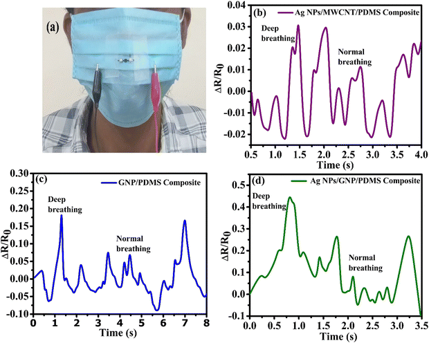
The strain sensors were mounted to the outer surface of the mask of a volunteer for the breathing tests. Stable and reliable variations in the resistance of the sensor are clearly observed during periodical breathing of the volunteer, as shown in Fig. 8(a)–(c). It may be mentioned here that human breathing analysis is a noninvasive technique to monitor consecutive breathing patterns for healthcare applications. From Fig. 8(a)–(c), the relative changes in resistance of the strain sensor clearly signify various breathing signals, viz. deep and normal breathing, thereby ensuring that it is a potential candidate for healthcare applications. Tensile as well as compressive strain are generated on the mounted sensor during human breathing. In the case of air exhale, micro cracks are formed in the nanocomposites leading to an increase in the resistance due to the generation of tensile strain, whereas air inhale resulting in compressive strain causes overlapping of the nanoflake layers. This promotes electron tunnelling facilitating the electron conductivity to increase.
 |
| | Fig. 8 (a) Optical image of a flexible piezo-resistive strain sensor mounted on the outer surface of the mask of a volunteer. The relative change in resistance of the sensors containing different nanocomposites: (b) Ag NP/MWCNT/PDMS, (c) GNP/PDMS and (d) Ag NP/GNP/PDMS corresponding to the breathing of the volunteer during testing. | |
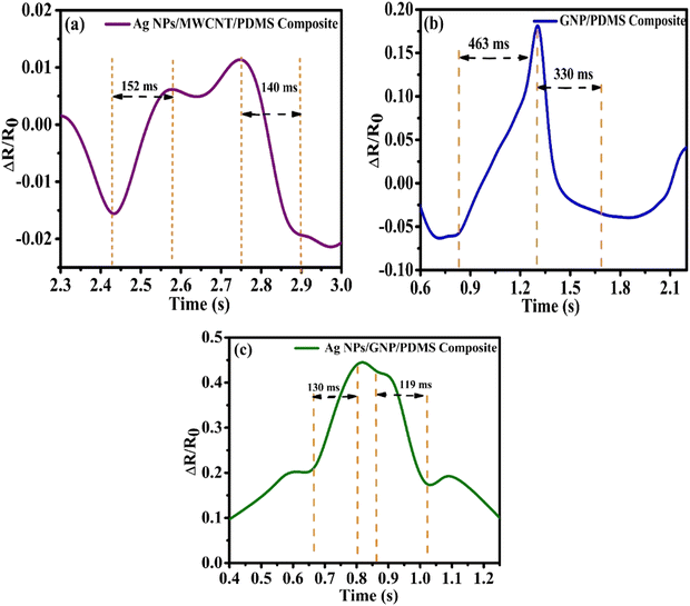
For practical applications, it is pertinent to determine the response and recovery time of the sensor. The response time of the fabricated sensor is determined by observing the variation of resistance during breathing/unbreathing conditions, as shown in Fig. 9. It is worth mentioning that the response and recovery time of all the sensors has been calculated under identical breathing/unbreathing conditions. The response time of the sensors based on different nanocomposites of Ag NP/MWCNT/PDMS, GNP/PDMS and Ag NP/GNP/PDMS are found to be 152, 463 and 130 ms, whereas the recovery time is calculated to be 140, 330 and 119 ms, respectively.
 |
| | Fig. 9 Estimation of response and recovery time of the fabricated sensors containing different types of nanocomposites (a) Ag NPs/MWCNT/PDMS, (b) GNP/PDMS and (c) Ag NPs/GNP/PDMS corresponding to the breathing of the volunteer during testing. | |
An optical image of the sensor mounted on a human hand during press/release tests is shown in Fig. 10(a). The finger tapping response of the composite based sensors is observed as shown in Fig. 10(b)–(d). When the sensor is pressed, a compressive strain is generated and thereby overlapping of the flakes promotes the electron flows easily. The resistance decreases again and when it is released it comes to its initial state and resistance increases. All the sensors are following the same trend but the response of the Ag NPs/GNP/PDMS composite shows a better sensitivity and it is similar to a rectangular waveform. In Table 2, a comparison of the results of the present study has been made with those reported earlier. The value of GF is found to be higher than those reported devices.
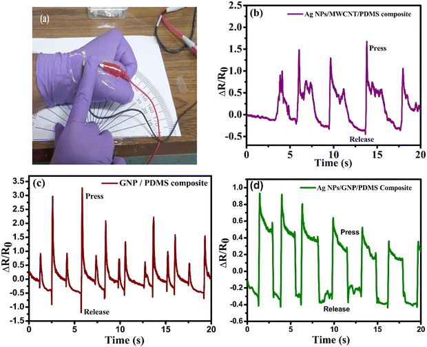 |
| | Fig. 10 (a) Optical photographs of the fabricated sensor mounted on the hand for tapping tests. The relative resistance changes of the different hybrid nanocomposites: (b) Ag NPs/MWCNT/PDMS, (c) GNP/PDMS and (d) Ag NPs/GNP/PDMS corresponding to the press and release cycle by the volunteer during testing. | |
Table 2 Comparison of performance in different flexible devices
| Material |
Methods |
Strain (%) |
Gauge factor |
Ref. |
| Graphene film on rubber |
Spray coating |
5 |
6–35 |
39
|
| Graphene rosette strain gauge on PDMS film |
Reactive ion etching, stamping |
7.1 |
14 |
40
|
| Graphene serpentine strain sensor on PDMS |
Chemical vapor deposition, photolithography, spray coating |
20 |
42.2 |
41
|
| Graphene thin film on PET substrate |
Spray deposition |
1.5 |
10–100 |
43
|
| GNP in microchannel on PDMS |
PDMS casting inside 3D-printed mould, graphene ink drop-casting |
±1.92 |
37 |
45
|
| GNP on PDMS |
Manual coating |
65 |
62.5 |
46
|
| 3D graphene foam |
CVD |
15 |
6.24 |
44
|
| Silver nanoparticles/SWCNT |
Screen printing |
20 |
76 |
34
|
| Ag NPs/MWCNT/PDMS; GNP/PDMS; Ag NPs/GNP/PDMS |
Manual coating |
0–15% |
188 |
Present study |
| 0–30% |
104 |
| 0–55% |
221 |
4 Conclusion
In conclusion, flexible piezo-resistive strain sensors were fabricated using silver nanoparticle (Ag NP), graphene nanoplatelet (GNP) and carbon nanotube (CNT) based hybrid nanocomposites with the help of a simple solution processing technique. The electrical characteristics of the flexible strain sensors with structures Ag NPs/MWCNT/PDMS, GNP/PDMS and Ag NPs/GNP/PDMS were systematically analyzed to study and understand the piezo-resistive behavior in these devices. The superior performance of the flexible sensors containing Ag NPs, GNP and PDMS is caused by the high surface area of the Ag NPs and GNPs resulting in uniform filling and distribution of Ag NPs into the porous GNP surface and thereby facilitating high contact area along with better electron transport. The GF, response and recovery time of the Ag NPs/GNP/PDMS hybrid nanocomposite-based sensors are found to be 221, 130 ms and 119 ms, respectively. Thus, with its simple structure, ease of device processing and fabrication, coupled with flexibility and reasonably good gauge factor comparable to the state-of-the-art devices, response and recovery time, it has tremendous promise in the field of wearable electronics.
Conflicts of interest
There are no conflicts to declare.
Acknowledgements
The authors gratefully acknowledge SERB, New Delhi, India for providing the support through a project (SPG/2021/003220). The authors also wish to thank Director, CSIR-CEERI for his constant motivation and cooperation throughout the work. The authors also gratefully acknowledge the R&D facility group, CSIR-CEERI, Pilani for device processing.
References
- T. Yang, X. Jiang, Y. Zhong, X. Zhao, S. Lin, J. Li, X. Li, J. Xu, Z. Li and H. Zhu, ACS Sens., 2017, 2, 967–974 CrossRef CAS PubMed.
- Y. Liu, H. Wang, W. Zhao, M. Zhang, H. Qin and Y. Xie, Sensors, 2018, 18, 645 CrossRef PubMed.
- I. Kang, M. J. Schulz, J. H. Kim, V. Shanov and D. Shi, Smart Mater. Struct., 2006, 15, 737 CrossRef CAS.
- Z. Yang, Y. Pang, X. L. Han, Y. Yang, J. Ling, M. Jian, Y. Zhang, Y. Yang and T. L. Ren, ACS Nano, 2018, 12, 9134–9141 CrossRef CAS PubMed.
- L. Q. Tao, K. N. Zhang, H. Tian, Y. Liu, D. Y. Wang, Y. Q. Chen, Y. Yang and T. L. Ren, ACS Nano, 2017, 11, 8790–8795 CrossRef CAS PubMed.
- S. Yaragalla, S. Dussoni, M. Zahid, M. Maggiali, G. Metta, A. Athanasiou and I. S. Bayer, J. Ind. Eng. Chem., 2021, 101, 348–358 CrossRef CAS.
- A. Georgopoulou, S. Michel, B. Vanderborght and F. Clemens, Sens. Actuators, A, 2021, 318, 112433 CrossRef CAS.
- Z. Ma, Y. Zhang, K. Zhang, H. Deng and Q. Fu, Nano Mater. Sci., 2023, 5, 265–277 CrossRef CAS.
- P. Cataldi, S. Dussoni, L. Ceseracciu, M. Maggiali, L. Natale, G. Metta, A. Athanassiou and I. Bayer, Adv. Sci., 2017, 5, 1700587 CrossRef PubMed.
- S. Saha, V. Yauvana, S. Chakraborty and D. Sanyal, Mater. Today, 2019, 18, 1450–1458 CAS.
- J. Cheng, Y. Mu, C. Liu, W. Yang, W. Liu, H. Wang, J. Wu, F. Hou, D. Hao, L. Cheng, B. Weng and Y. Chen, IEEE Sens. J., 2022, 22, 18143–18150 CAS.
- H. Zhao and J. Bai, ACS Appl. Mater. Interfaces, 2015, 7(18), 9652–9659 CrossRef CAS PubMed.
- T. Gong, J. Jia, X. Sun, W. Li, K. Ke, R. Bao and W. Yang, Carbon, 2023, 206, 53–61 CrossRef CAS.
- Q. Chen, H. Chen, Y. Liu, Z. Gao, B. Wu, X. Fan, C. Liu, H. Li, Y. Li and M. Ma, Infrared Phys. Technol., 2022, 127, 104387 CrossRef.
- A. L. Junior, L. Avellar, C. Marques and A. Frizera, IEEE Sens. J., 2022, 22, 2237–2243 Search PubMed.
- X. Zhenyuan, D. Zhang, Z. Li, C. Du, Y. Yang, B. Zhang and W. Zhao, ACS Appl. Mater. Interfaces, 2023, 15(27), 32569–32579 CrossRef PubMed.
- H. Cai, D. Zhang, H. Zhang, M. Tang, Z. Xu, H. Xia, K. Li and J. Wang, Chem. Eng. J., 2023, 472, 144849 CrossRef CAS.
- X. Chen, D. Zhang, H. Luan, C. Yang, W. Yan and W. Liu, ACS Appl. Mater. Interfaces, 2023, 15(1), 2043–2053 CrossRef CAS PubMed.
- C. Yang, D. Zhang, D. Wang, H. Luan, X. Chen and W. Yan, ACS Appl. Mater. Interfaces, 2023, 15(4), 5811–5821 CrossRef CAS PubMed.
- D. Wang, D. Zhang, M. Tang, H. Zhang, F. Chen, T. Wang, Z. Li and P. Zhao, Chem. Eng. J., 2022, 446, 136914 CrossRef CAS.
- R. Wu, L. Ma, S. Liu, A. B. Patil, C. Hou, Y. Zhang, W. Zhang, R. Yu, W. Yu, W. Guo and X. Y. Liu, Mater. Today Phys., 2020, 15, 100243 CrossRef.
- J. Li, L. Fang, B. Sun, X. Li and S. H. Kang, J. Electrochem. Soc., 2020, 167, 037561 CrossRef CAS.
- Y. Ling, X. Zhuang, Z. Xu, Y. Xie, X. Zhu, Y. Xu, B. Sun, J. Lin, Y. Zhang and Z. Yan, ACS Nano, 2018, 12, 12456–12463 CrossRef CAS PubMed.
- K. Gao, Z. Zhang, S. Weng, H. Zhu, H. Yu and T. Peng, Appl. Sci., 2022, 12, 9750 CrossRef CAS.
- I. Miranda, A. Souza, P. Sousa, J. Ribeiro, E. M. S. Castanheira, R. Lima and G. Minas, J. Funct. Biomater., 2022, 13, 2 CrossRef CAS PubMed.
- E. Berthier, E. W. K. Young and D. Beebe, Lab Chip, 2012, 12, 1224–1237 RSC.
- J. Zhao, D. A. Sheadel and W. Xue, Sens. Actuators, A, 2012, 187, 43–49 CrossRef CAS.
- J. Zhou, A. V. Ellis and N. H. Voelcker, Electrophoresis, 2010, 31, 2–16 CrossRef CAS PubMed.
- A. Mata, A. J. Fleischman and S. Roy, Biomed. Microdevices, 2005, 7, 281–293 CrossRef CAS PubMed.
- I. D. Johnston, D. K. McCluskey, C. K. L. Tan and M. C. Tracey, J. Micromech. Microeng., 2014, 24, 035017 CrossRef CAS.
- A. Victor, J. Ribeiro and F. F. Araújo, J. Mech. Eng. Biomech., 2019, 4, 1–9 CrossRef.
- C. Cardoso, C. S. Fernandes, R. Lima and J. Ribeiro, Mech. Res. Commun., 2018, 90, 26–33 CrossRef.
- J. W. Lee, J. Y. Cho, M. J. Kim, J. H. Kim, J. H. Park, S. Y. Jeong, S. H. Seo, G. W. Lee, H. J. Jeong and J. T. Han, Sci. Rep., 2021, 11, 5140 CrossRef CAS PubMed.
- G. Y. Lee, M. S. Kim, S. H. Min, H. S. Kim, H. J. Kim, R. Keller, J. B. Ihn and S. H. Ahn, ACS Appl. Mater. Interfaces, 2019, 11, 26421–26432 CrossRef CAS PubMed.
- M. A. U. Khalid and S. H. Chang, Compos. Struct., 2022, 284, 115214 CrossRef CAS.
- B. Nie, X. Li, J. Shao, X. Li, H. Tian, D. Wang, Q. Zhang and B. Lu, ACS Appl. Mater. Interfaces, 2017, 9, 40681–40689 CrossRef CAS PubMed.
- M. A. Darabi, A. Khosrozadeh, Q. Wang and M. Xing, ACS Appl. Mater. Interfaces, 2015, 7, 26195–26205 CrossRef CAS PubMed.
- S. Baloda, N. Gupta and S. Singh, IEEE Trans. Electron Devices, 2022, 69(12), 7011–7018 CAS.
- Y. Liu, D. Zhang, K. Wang, Y. Liu and Y. Shang, Composites, Part A, 2016, 80, 95–103 CrossRef CAS.
- S. H. Bae, Y. Lee, B. K. Sharma, H. J. Lee, J. H. Kim and J. H. Ahn, Carbon, 2013, 51, 236–242 CrossRef CAS.
- S. Chun, Y. Choi and W. Park, Carbon, 2017, 116, 753–759 CrossRef CAS.
- A. Khan, S. M. Islam, S. Ahmed, R. R. Kumar, M. R. Habib, K. Huang, M. Hu, X. Yu and D. Yang, Adv. Sci., 2018, 1800050, 1–29 Search PubMed.
- R. Get, S. M. Islam, S. Singh and P. Mahala, Microelectron. Eng., 2020, 222, 111200 CrossRef CAS.
- R. Get, S. M. Islam, S. Singh and P. Mahala, Optik, 2022, 266, 169560 CrossRef CAS.
- M. Hempel, D. Nezich, J. Kong and M. Hofmann, Nano Lett., 2012, 12, 5714–5718 CrossRef CAS PubMed.
- R. Xu, Y. Lu, C. Jiang, J. Chen, P. Mao, G. Gao, L. Zhang and S. Wu, ACS Appl. Mater. Interfaces, 2014, 6, 13455–13460 CrossRef CAS PubMed.
- A. M. Kamat, Y. Pei and A. Kottapalli, Nanomaterials, 2019, 9, 954 CrossRef CAS PubMed.
- S. Baloda, Z. A. Ansari, S. Singh and N. Gupta, IEEE Sens. J., 2022, 20, 13302–13309 Search PubMed.
- D. Sethy and K. Balasubramaniam, Materials, 2022, 15, 3924 CrossRef CAS PubMed.
- A. Khan, M. R. Habib, R. R. Kumar, S. M. Islam, V. Arivazhagan, M. Salman, D. Yang and X. Yu, J. Mater. Chem. A, 2018, 6, 22437 RSC.
- F. Yin, D. Ye, C. Zhu, L. Qiu and Y. Huang, Sensors, 2017, 17, 2677 CrossRef PubMed.
- A. Raza, S. Altaf, S. Ali, M. Ikram and G. Li, Sustainable Mater. Technol., 2022, 32, e00406 CrossRef CAS.
- S. Moeen, M. Ikram, A. Haider, J. Haider, A. Ul-Hamid, W. Nabgan, T. Shujah, M. Naz and I. Shahzadi, ACS Omega, 2022, 7, 46428–46439 CrossRef CAS PubMed.
- Ayesha, M. Imran, A. Haider, I. Shahzadi, S. Moeen, A. Ul-Hamid, W. Nabgan, A. Shahzadi, T. Alshahrani and M. Ikram, J. Environ. Chem. Eng., 2023, 11, 110088 CrossRef CAS.
- A. Shahzadi, S. Moeen, A. D. Khan, A. Haider, J. Haider, A. Ul-Hamid, W. Nabgan, I. Shahzadi, M. Ikram and A. Al-Shanini, ACS Omega, 2023, 8, 8605–8616 CrossRef CAS PubMed.
- M. Ikram, A. Haider, M. Imran, J. Haider, S. Naz, A. Ul-Hamid, A. Shahzadi, S. Moeen, G. Nazir, W. Nabgan, A. Bashir and S. Ali, Surf. Interfaces, 2023, 37, 102710 CrossRef CAS.
- M. Ikram, A. Haider, M. Imran, J. Haider, S. Naz, A. Ul-Hamid, A. Shahzadi, K. Ghazanfar, W. Nabgan, S. Moeen and S. Ali, Int. J. Biol. Macromol., 2023, 230, 123190 CrossRef CAS PubMed.
- M. Ikram, A. Haider, S. T. Bibi, A. Ul-Hamid, J. Haider, I. Shahzadi, W. Nabgan, S. Moeen, S. Ali, S. Goumri-Said and M. B. Kanoun, RSC Adv., 2022, 12, 32142–32155 RSC.
- F. Jamal, A. Rafique, S. Moeen, J. Haider, W. Nabgan, A. Haider, M. Imran, G. Nazir, M. Alhassan, M. Ikram, Q. Khan, G. Ali, M. Khan, W. Ahmad and M. Maqbool, ACS Appl. Nano Mater., 2023, 6(9), 7077–7106 CrossRef CAS.
- M. H. Ali, M. A. K. Azad, K. A. Khan, M. O. Rahman, U. Chakma and A. Kumer, ACS Omega, 2023, 8(31), 28133–28142 CrossRef CAS PubMed.
- N. Radhakrishnan and C. B. Sobhan, Heat Mass Transf., 2022, 58, 1811–1828 CrossRef CAS.
|
| This journal is © the Owner Societies 2024 |
Click here to see how this site uses Cookies. View our privacy policy here. 
 a,
Sk.
Masiul Islam
a,
Sk.
Masiul Islam