
Rock-salt Ti1−xO → rutile TiO2−x transformation twinning via pulsed laser deposition – implications for the dense (hkl)-specific phase change and optoelectronic properties†
Chang-Ning
Huang
 *a,
Jian-Yu
Chen
a,
Yu-Xuan
Lin
a and
Pouyan
Shen
b
*a,
Jian-Yu
Chen
a,
Yu-Xuan
Lin
a and
Pouyan
Shen
b
aDepartment of Chemical and Materials Engineering, Southern Taiwan University of Science and Technology, Tainan 710301, Taiwan, Republic of China. E-mail: cnhuang@stust.edu.tw
bDepartment of Materials and Optoelectronic Science, National Sun Yat-sen University, Kaohsiung 80424, Taiwan, Republic of China
First published on 29th February 2024
Abstract
Defective rock-salt (R) Ti1−xO → rutile (r) TiO2−x transformation twinning occurred in a thin film with preferred shape and crystallographic orientation when deposited on silica glass substrates, with or without a coating of fluorine-doped tin oxide, using pulsed laser ablation of a rutile polycrystal under specific pulse energies in the range of 200 to 800 mJ per pulse in vacuum. The films were characterized by X-ray diffraction and electron microscopy and shown to contain nanocrystallites of R, r, and minor high-temperature-stabilized hexagonal Ti1−xO all with preferred orientations adopted by close-packed planes. The R + r intimate intergrowth was found to form a butterfly twin following the optimum crystallographic orientation relationship [101]R//[11![[1 with combining macron]](https://www.rsc.org/images/entities/char_0031_0304.gif) ]r with close-packed (11)R and (011)r planes as the twin boundary and phase interface with a fair 2-D coincidence site lattice in accordance with the dense (111)R-specific R → r transformation route. The R + r predominant film with aliovalent point defects and paracrystalline distribution of defect clusters showed characteristic white light absorbance, violet + green double emission, and fine photoelectron chemical properties for potential photovoltaic, photocatalytic, and optoelectronic applications, in particular for multiple temperature- and oxygen-fugacity sensors in terms of the R → r transformation.
]r with close-packed (11)R and (011)r planes as the twin boundary and phase interface with a fair 2-D coincidence site lattice in accordance with the dense (111)R-specific R → r transformation route. The R + r predominant film with aliovalent point defects and paracrystalline distribution of defect clusters showed characteristic white light absorbance, violet + green double emission, and fine photoelectron chemical properties for potential photovoltaic, photocatalytic, and optoelectronic applications, in particular for multiple temperature- and oxygen-fugacity sensors in terms of the R → r transformation.
Introduction
Titanium oxides have various crystal structures and stoichiometries, and hence multiple cation charges in terms of Ti:O atomic ratios.1 Their synthesis and mutual transformations to form specific structures, sizes, shapes, and space-charged defects are of particular interest with regard to their photocatalytic/photoelectrochemical properties2 and superconductivity.3,4 Besides the wet chemical sol–gel synthesis of some TiO2 powders in the form of anatase and/or rutile for commercial purposes or fundamental research,5,6 the physical–chemical evaporation method is commonly used to deposit a thin titanium oxide film on some substrates, under specific temperature and oxygen-fugacity conditions.7,8 In the transparent conductive oxide glass category, fluorite-doped tin oxide (FTO)-coated glass has been widely used as a substrate for facile photocatalytic and photoelectrochemical applications of the overlying film.9Pulsed laser ablation (PLA) of a Ti metal target in specific environmental conditions is a powerful physical–chemical evaporation method used to fabricate various kinds of titanium oxides. For example, high-pressure polymorphs of TiO2 with an α-PbO2-type (space group Pbcn) structure10 and baddeleyite-type (MI, fluorite-related type P21/c) TiO2 (ref. 11) were synthesized via very energetic Nd-YAG laser pulse irradiation of the oxygen-purged Ti target under very rapid heating and cooling for a significant shock effect. Such dense polymorphs of TiO2 occur in nature only above 4 to 5 GPa at 900 °C to 1000 °C in an ultrahigh-pressure (UHP) metamorphic terrain.12 In another study, ambient-pressure-stabilized anatase (space group I41/amd) and rutile (space group P42/mnm) nanoparticles were fabricated by PLA of the Ti target under a specific pulse energy and oxygen flow rate.13 Such rutile nanoparticles were found to have well-developed {110} and {011} surfaces with steps for {∼110} and {∼011} vicinal attachment, causing, respectively, edge dislocations and planar defects (fault and twin) in the rutile crystal.14 Topologically, a displacement vector  of 0.5[01] parallel to the (011) plane results in an intrinsic fault, and a further successive fault ends up with an extrinsic fault (cf.Fig. 6c and d in Tsai et al., 2004).14
Conversely, titanium oxide compounds Ti1−xO, Ti2O3, and TiO2 with a considerable extent of nonstoichiometry (x) as fabricated by PLA in water were protonated and have a relatively high content of Ti2+ for a lower minimum band gap of 3.4 eV, as well as Ti vacancies and charge/volume-compensating defects for potential optoelectronic and catalytic applications in the UV-visible range.15 In contrast, C–H doped anatase nanospheres with disordered shells and planar defects were topotaxially formed from rock-salt-type TiCxOy and β-Ti nuclei with a paracrystalline distribution of defect clusters upon PLA of bulk Ti in tetraethyl orthosilicate.16 In this connection, the stoichiometric rock-salt TiO (space group Fm![[3 with combining macron]](https://www.rsc.org/images/entities/char_0033_0304.gif) m), as synthesized by reacting KClO4 with elemental Ti in a sealed and evacuated quartz tube, was reported to have a rather large lattice parameter of 0.4228 nm and hence an enhanced superconductivity transition temperature of 5.5 K.4
m), as synthesized by reacting KClO4 with elemental Ti in a sealed and evacuated quartz tube, was reported to have a rather large lattice parameter of 0.4228 nm and hence an enhanced superconductivity transition temperature of 5.5 K.4
With regard to protoxide to dioxide transformation, a Ti film deposited on a NaCl (001) surface was subjected to thermal oxidation in air at 350 °C to form TiO and at 400 °C for partial transformation into anatase (A) following the parallel crystallographic orientation relationship (COR) {200}A//{200}TiO in accordance with the similarity of the oxygen sublattice (cf.Fig. 8 in Kao et al. 2011)17 (in fact, the TiO → anatase transformation involves about one-half of Ti2+ ions being removed from the TiO cell coupled with the remaining Ti2+ ions being oxidized into Ti4+ ions and a slight shift in O2− ions (Kao et al. 2011)17). In contrast, the backward anatase to TiO transformation was recently achieved by in situ heating in a vacuum (10−3 Pa) during electron microscopic observations in the temperature range of 950–1200 °C (Chen et al., 2022)18 (note the quote from Chen et al. (2022):18 “When the heating took place in the vacuum chamber, the overall pressure (about 10−3 Pa) is not as low as that in the microscope (about 10−6 Pa)”). The rock-salt TiO nanoparticles thus produced from anatase nanorods are cuboctahedral in shape and immune to dislocation (cf.Fig. 4 in Chen et al., 2022),18 although the lattice parameter and hence a possible deviation from TiO stoichiometry were not measured.
Herein, PLA deposition of a Ti1−xO + TiO2−x composite film on a substrate of silica glass with or without an FTO coating was accomplished by laser irradiation of a sintered rutile polycrystal at specific pulse energies in vacuum. We focused on the (hkl)-specific orientation of the phase assemblage and pulse-energy dependent lattice parameters of predominant Ti1−xO and TiO2−x that enabled the novel rock-salt Ti1−xO → rutile TiO2−x transformation with optimum COR and a fair lattice match. The size, shape, and planar defects of nanocondensates in terms of the close-packed planes and cluster of point defects with aliovalent charges were characterized with regard to measured UV-visible, photoluminescence, and photoelectrochemical properties for potential sensor applications.
Experimental
Materials preparation
Reagent-grade TiO2 (rutile type, Alfa Aesar, 99.5%, 325 mesh) powders were ground and dry pressed at 650 MPa into a disk ca. 20 mm in diameter and 0.5 mm in thickness. The green disk was then sintered at 1200 °C for 12 h at the rate of 5 °C min−1 in an Ar atmosphere. It was then cooled to room temperature in a tube furnace. The disks of rutile polycrystal (ca. 1 to 10 μm in grain size with point defects and hence an iron grayish color) thus obtained were subjected to pulse irradiation from an energetic Nd-YAG-laser (Quantel smart 850, 1064 nm in wavelength, beam mode: TEM00) in vacuum (8 × 10⁵ torr). A laser beam was focused down to a diameter of 3 mm on the rotating target with a working distance of 5 cm under laser pulse energy of 200–800 mJ per pulse using 1064 nm excitation to achieve a peak power density of 4.7 × 10⁸ to 1.8 × 10⁹ W cm−2, given a pulse time duration of 6 ns at 10 Hz under the Q-switch mode. The 30 min PLA runs were employed to deposit thin films on the substrate of FTO-coated silica glass or FTO-free silica glass for further microscopic and spectroscopic analysis of deposits. The detailed laser parameters and resultant phase abundance are listed in Table 1.| Sample number | 1 | 2 | 3 | 4 |
|---|---|---|---|---|
| Wavelength (nm) | 1064 | 1064 | 1064 | 1064 |
| Mode | Q-switch | Q-switch | Q-switch | Q-switch |
| Pulse energy (mJ per pulse) | 200 | 400 | 600 | 800 |
| Pulse duration (ns) | 6 | 6 | 6 | 6 |
| Frequency (Hz) | 10 | 10 | 10 | 10 |
| Beam size (mm2) | 7 | 7 | 7 | 7 |
| Peak power (W) | 1.3 × 10⁷ | 6.5 × 10⁷ | 9.8 × 10⁷ | 1.3 × 10⁸ |
| Power density (W cm−2) | 4.7 × 10⁷ | 9.4 × 10⁸ | 1.4 × 10⁹ | 1.8 × 10⁹ |
| Deposition time (min) | 30 | 30 | 30 | 30 |
| Phase relative abundance | R > a > H ≫ r | R > a > H ≫ r | R∼r > H ≫ a | r∼R∼a > H |
Characterization of the materials
An X-ray diffraction (XRD, Cu Kα at 40 kV and 40 mA) study using the method of grazing incidence wide-angle X-ray scattering (GIWAXS, Bruker AXS D8 Discovery instrument) coupled with a GADDS area detector was employed to identify crystalline phases in the thin film deposited on a transparent glass substrate with or without FTO coating. The thin film deposited on optically transparent FTO glass was characterized by polarized light microscopy (Nikon Eclipse LV100N POL), with a focus on the condensates under open and/or cross-polarizers regarding their agglomeration, crystallinity, and orientation. Scanning electron microscopy (SEM, JEOL JSM-6701F,10 kV) coupled with secondary electron image (SEI) and energy dispersive X-ray (EDX) analysis was used for further analyses of microstructure and chemical composition of the condensates in the films.The thin film, as deposited on FTO-silica glass, was cross-cut into thin sections by a focused ion beam (FIB, using an FEI Helios G3 CX system, 30 kV) and was then settled on the copper grid with a carbon-coated collodion film for further characterization of composition distribution and crystal structure/shape using transmission electron microscopy (TEM, JEOL JEM-2100F Cs STEM at 200 kV) coupled with bright field image (BFI), selected area electron diffraction (SAED) and point-count energy dispersive X-ray (EDX) analysis at a beam size of 1 nm. The Z-contrast images coupled with compositional line scanning profiles were acquired with a high-angle annular dark-field (HAADF) detector and EDX under STEM mode. Lattice images coupled with 2-D forward Fourier transform (FFT) were taken to identify the definite COR of the phase assemblage with (hkl)-specific interfaces due to particle impingement and/or phase transformation.
The electron energy loss spectrum (EELS), as acquired from a Gatan image filter coupled with TEM, was employed to identify the chemical bonding state of the titanium oxides in the FIB section. The powdery samples were also examined by X-ray photoelectron spectroscopy (XPS, PHI 5000 Versa Probe with monochromatized Al Kα radiation of 1486.6 eV) calibrated with a standard of C 1s at 284 eV for the determination of Ti2+, Ti3+, and Ti4+ peaks. A UV-vis (HITACHI U4100) spectrometer coupled with an integrating sphere was used to measure light absorption in the range of 190–900 nm for the determination of the band gap of the deposit on the FTO-silica glass by the Tauc plot method. For vibrational and photoluminescence (PL) studies, micro-Raman/PL spectroscopy (HORIBA Labram HR) under 325 nm and 532 nm excitation by a He–Cd and a diode laser with 1 μm spatial resolution were employed, respectively.
A potentiostat (Metrohm Autolab PGSTAT30) with a three-electrode electrochemical cell, with Pt as the counter electrode, Ag/AgCl as the reference electrode, Ti1−xO + TiO2−x/FTO film as the working electrode, and 0.1 M KOH (pH = 13.1) as an electrolyte solution was employed to measure cyclic voltammograms and the current density-time curve at 1.2 V under xenon lamp irradiation.
Results
XRD measurements
XRD from thin films deposited on the FTO-coated silica glass (Fig. 1a) showed strong diffraction from a cassiterite polycrystal in FTO, but there was negligible diffraction from the films, as otherwise isostructural rutile peaks shifting to higher 2θ angle (cf. dashed lines) and diffraction of other titanium oxide phases would be observed. Apparently, a total of 30 min PLA time was not long enough to accumulate XRD-appreciable crystallites on the FTO-silica glass, despite using the advanced 2-D GIWAX technique. This indicates a significant interdiffusion reaction with FTO to consume the films during the PLA process. | ||
| Fig. 1 XRD traces of titanium oxide thin films as deposited on the substrates of (a) FTO-coated silica glass and (b) silica glass by the PLA process for 30 min in vacuum under 200, 400, 600, and 800 mJ per pulse, respectively. Note that R-Ti1−xO and r-TiO2−x condensates are not concentrated enough in the film to show appreciable diffraction, in contrast with the overwhelming signals of cassiterite polycrystals from the FTO underneath in (a). | ||
In contrast, the two relatively strong yet broad (111) and (200) diffractions of rock-salt (hereafter denoted R) Ti1−xO were unambiguously identified from the films as deposited on FTO-free silica glass at all the pulse energies adopted (Fig. 1b). The preferred orientation of R-Ti1−xO in such films adopted by the close-packed (111)R plane is manifested by a much higher intensity ratio of I111R/I200R = 2 in comparison with 0.5 for the random powder diffraction data of TiO (JCPDS file 65-2900). It should be noted that a minor additional phase (denoted as H, space group P6/mmm, JCPDS file 85-2084) of Ti1−xO confirmed by TEM observations is different from three TiO phases (α, β, and γ) with defective NaCl-type structures of lower crystal symmetry (Amano et al., 2016);19 it tended to survive the PLA process at pulse energy as high as 800 mJ per pulse. The (111)R diffraction peak shifts progressively toward a higher 2θ angle, i.e. a smaller d-spacing approaching that (0.241 nm) of TiO with supposed stoichiometry (JCPDS file 65-2900) when the pulse energy increases from 200 to 600 mJ per pulse. The corresponding lattice parameter (0.4180 nm) is significantly smaller than 0.4228 nm for stoichiometric TiO (Wang et al., 2017),4 indicating a considerable extent of nonstoichiometry (x). Such a nonstoichiometric state of R-Ti1−xO was sustained despite significant amorphization and oxidation transformation into dioxide at a high pulse energy of 800 mJ per pulse.
As for rutile (denoted r) TiO2−x, it shows (101)r, (202)r, and (212)r diffractions in the XRD trace for the film fabricated at 600 mJ per pulse (Fig. 1b) due to the preferred orientation adopted by the close-packed (101)r plane, i.e. with close-packed layers lying parallel to the substrate. There is a slightly larger d-spacing (+0.001 nm) for the present r-TiO2−x nanocondensates than that documented for rutile TiO2 (JCPDS file 21-1276), presumably due to doped Ti2+ (0.086 nm) and Ti3+ (0.067 nm) having relatively large effective radii in coordination number (CN) 6 (Shannon, 1976).20 The preferred orientation of r-TiO2−x remained, and the broad scatter intensity below the 25° 2θ angle of the amorphous phase was enhanced for the film fabricated at the highest pulse energy of 800 mJ per pulse. This indicates that 600 mJ per pulse is the optimum pulse energy, which gives the best yield of R-Ti1−xO and r-TiO2−x, although with significant strain broadening of XRD peaks due to the combined effects of x, miniature size, and defects. Beyond such a threshold, further transformation of R-Ti1−xO into r-TiO2−x and the amorphous phase occurred (the XRD results from the 2-D GIWAX analysis are basically the same for the film samples as prepared in three different runs of PLA deposition on silica glass in a vacuum). In fact, there is a different relative abundance of the amorphous phase, H-Ti1−xO, R-Ti1−xO and r-TiO2−x (cf.Table 1) according to XRD and later TEM observations on the films, which increase in thickness linearly from 0.1 to 0.5 μm (SEM cross-section measurements) as the pulse energy increases from 200 to 800 mJ per pulse.
Optical microscopy and SEM observations
The film transparency decreases with an increase in the pulse energy used for PLA deposition on FTO-glass, regardless of the subsequent annealing at 450 °C for 5 h in air (Fig. S1†). The drastic color change from gray to dark brownish for the samples produced above 200 mJ per pulse indicates a significant phase and/or defect change of the condensates in the films. Optical polarized microscopic observations on such glass slides overlain with film under reflective light or transmitted light with open/cross polarizers, and an optical retardation λ plate (Fig. S2†) showed noncubic crystals up to micron size with significant interference color. They are mainly columnar cassiterite grains in FTO, and there are occasional rutile TiO2−x particulates in the films, although the nanocondensates are too fine to be resolved by optical microscopy. The occurrence of rutile TiO2−x particulates with optical birefringence was confirmed by optical polarized microscopic observations on the films as deposited on FTO-free silica glass (Fig. S3†).Top-view SEM SEI indicates that the film deposited on FTO-coated silica glass in vacuum consists of 100–300 nm-scale agglomerates, which are composed of faceted nanocondensates of ca. tens of nm in size, as represented by the sample produced under 200 mJ per pulse for 30 min (Fig. 2a). The nanocrystallites are mainly R-Ti1−xO with the preferred orientation of the close-packed plane to enable further transformation into r-TiO2−x at higher pulse energy according to XRD and later TEM identification (the so-called artificial epitaxy of crystallites on the amorphous substrate is also related to the preferred orientation of the crystallites adopted by the close-packed plane21 and references therein). The nanocrystallites were significantly sintered to form triple junctions typical of a solid-state sintering process and coarsened to ca. 50–100 nm in size after annealing at 450 °C for 5 h in air (Fig. 2b). The occasional pores in Fig. 2b indicate that the sintering process was incomplete after this heating treatment. The microstructures of the other film samples (i.e. those prepared under 400, 600, and 800 mJ per pulse) are basically the same (not shown).
 | ||
| Fig. 2 Top-view SEM SEI of the titanium oxide thin film (a) as deposited on FTO-coated silica glass under 200 mJ per pulse for 30 min in vacuum and (b) after annealing at 450 °C for 5 h in air. | ||
STEM and TEM observations
The STEM results for a thin film deposited on the FTO-glass by PLA of a rutile polycrystal target are compiled in Fig. 3, with the representative case of PLA under 600 mJ per pulse. The HAADF image (Fig. 3a) coupled with EDX mapping (Fig. 3b–e for Ti Kα1, Sn Lα1, Si Kα1, and O Kα1 signals, respectively) and line scanning showed a higher Z-contrast of FTO and significant Ti inward and Sn outward diffusion in a narrow zone, ca. 50 nm in thickness, across the film/FTO boundary. There was also a similar Sn/Si interdiffusion zone across the FTO/silica boundary. In contrast, there is a monotonous trend of oxygen outward diffusion throughout the cross-section of film/FTO/silica to act as a directional oxygen supply for the titanium oxide film. Apparently, the FTO-silica glass substrate was significantly heated up by the PLA deposition process to activate not only diffusion bonding but also oxidation of the accumulating condensates. A film thus deposited under the highest pulse energy of 800 mJ per pulse, as another example (Fig. S4 and S5†), also showed Ti/Sn interdiffusion within a zone of ca. 100 μm in width. Again, there is significant monotonous oxygen outward diffusion toward the free surface of the film, which is made of fine nanocondensates in drastic contrast to large (hundreds of nm, cf. Fig. S4†) columnar cassiterite grains in FTO. The oxygen concentration profiles for the two representative samples indicate that the condensates partially oxidized by the PLA process with a rutile TiO2 target were further oxidized by the oxygen uptake from the FTO-coated silica glass. | ||
| Fig. 3 Compiled STEM results of the titanium oxide thin film as deposited on FTO-coated silica glass by the PLA process under 600 mJ per pulse in vacuum: (a) HAADF image; (b)–(e) EDX mapping and (f) EDX line scan from position A to B in (a), showing Ti inward and Sn outward diffusion in a narrow (ca. 50 nm thick) interdiffusion zone. | ||
TEM BFI coupled with the SAED pattern and point EDX spectrum (Fig. 4a–c) showed further structural and compositional details of the thin film as deposited on the FTO-glass at 600 mJ per pulse as an example. The predominant R-Ti1−xO and minor r-TiO2−x nanocondensates are ca. 5 to 30 nm in size and more or less coalesced with significant preferred orientations, as indicated by the diffraction arcs of R phase (i.e. {200}R and {220}R arcs and conjugated {111}R diffractions of 70.5° twin variants in Fig. 4b). There is also an amorphous phase to account for the diffuse scattering intensity. The enlarged BFI shows more clearly the coalesced nanocrystals of R-Ti1−xO and genicular rutile TiO2−x in accordance with the 135.0° twin law (cf. Fig. S6†). The microstructures and phase assemblage are generally similar for the films deposited under other pulse energy conditions, despite the difference in relative abundance of the phases (cf. Fig. S7† for the case of 200 mJ per pulse with an abundant amorphous phase). Further lattice imaging showed that additional high temperature favored the H-Ti1−xO phase (Fig. S8†) according to the documented case of H-TiO (JCPDS file 85-2084). The amorphous phase is abundant and has strong diffuse electron intensity for a film fabricated under the highest pulse energy of 800 mJ per pulse, as compiled in the “phase relative abundance” item in Table 1. The point-count EDX analyses on the intimately mixed R-Ti1−xO and r-TiO2−x qualitatively showed the Ti/O point count ratios varying from place to place with negligible Sn and F counts (Fig. 4c).
 | ||
| Fig. 4 TEM images of (a) BFI coupled with (b) SAED pattern and (c) EDX spectrum of the titania oxide thin film (predominantly R-Ti1−xO with preferred orientation and minor r-TiO2−x) as deposited on FTO-coated silica glass by the PLA process under 600 mJ per pulse in vacuum. | ||
The TEM lattice image (Fig. 5a) coupled with a 2-D forward Fourier transform (FFT) (inset) from the magnified region of interest (Fig. 5b) shows the defective rock-salt Ti1−xO nanocondensate, as produced by 200 mJ per pulse as an example. The defect is about dislocation with a (100) half-plane edge-on in the [001]R zone axis, presumably due to the coalescence of nanocondensates on the ∼(100) vicinal surface. Sideband (SB) diffractions around the fundamental diffractions of rock-salt Ti1−xO can be attributed to the paracrystalline distribution of defect clusters with an average interspacing of ca. 2.5 times the lattice parameter of the rock-salt structure, as addressed latter. The low-magnification TEM BFI (Fig. S9†) shows the overall view of the defective region with distinct wavefront contrasts, which are attributed to a combination of dislocations and defect clusters.
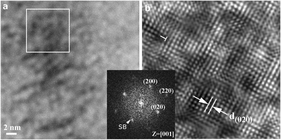 | ||
| Fig. 5 TEM (a) lattice image of the R-Ti1−xO rich domain and (b) magnified square region with FFT (inset) showing dislocation (⊥) and paracrystalline distribution of defect clusters with an interspacing ca. 5 times (020) lattice fringes corresponding to sideband (SB) diffractions in the [001]R zone axis. FIB sample from a film deposited on the FTO-coated silica glass under 200 mJ per pulse. | ||
The lattice image (Fig. 6a) and magnified region of interest (Fig. 6b) from the film produced under 200 mJ per pulse, as an example, showed the novel rutile TiO2−x/rock-salt Ti1−xO nanocomposite with planar defects. They occurred amazingly as butterfly twin bicrystals following optimum COR [101]R//[11]r with (11)R//(011)r as the shared twin boundary edge-on in the [101]R/[11]r zone axis. This twinned composite accounts for superimposed twin spots from the two phases and double diffractions in the zone axis, as confirmed by the 2D-FFT with schematic indexing in the reciprocal lattice (Fig. 6c) and 2-D inverse Fourier transform (IFFT) from the individual phases in Fig. 6d and e, respectively. There are stacking faults (intrinsic with displacement vector  = 0.5[01]r) near the twin boundaries and well-developed {110}r faces, as shown edge-on in the [101]R/[11]r zone axis. Note that the rutile twin variants are shown by the opposite lattice fringes across the (011)r twin boundary in Fig. 6d, whereas the rock-salt Ti1−xO twin variants shown by the opposite lattice fringes across the (111)R twin boundary in Fig. 6e are obscured by the partial transformation into r-TiO2−x and accompanying conjugated {111}R faulting and deformation twinning. The magnified images of Fig. 6d and e (Fig. S10†) indicate that the secondary polysynthetic twins of the butterfly bicrystal belong mainly to the parental R-Ti1−xO. In contrast, the intimate intergrowth of r-TiO2−x shows a closure twin associated with abundant dislocations and stacking faults. In contrast, the edge of the butterfly bicrystal is dominated by r-TiO2−x, which shows its well-developed {110}r faces edge-on (Fig. 6a).
 | ||
| Fig. 6 TEM (a) lattice image and (b) magnified square region of the r-TiO2−x/R-Ti1−xO nanocomposite following COR [101]R//[11]r; (11)R//(011)r as a butterfly twin bicrystal showing stacking faults (SF) near the twin boundary (TB) and well-developed {110}r faces edge-on in the [101]R/[11]r zone axis. (c) IFT of the square region with schematic indexing showing superimposed twin spots and double diffractions due to an intimate mixture of the two phases as further indicated by the IFFT of the individual phases in (d) and (e). FIB sample from the film deposited on the FTO-coated silica glass under 200 mJ per pulse. Note that the phantom (11)R//(011)r interface, as denoted by the white dashed line in (b), is obscured by the secondary deformation TBs of R and r phases (cf. text). | ||
The R → r transformation twinning could proceed by topotaxial nucleation of r at the (11)R twin boundary or surface to form a (011)r twin boundary. In any case, the original (11)R surface and (11)R//(011)r interface became obscured by the secondary deformation twins and faults of R and r phases for beneficial lower strain energy. As discussed later, the composite butterfly twin is remarkable with regard to the fact that the protoxide nanocondensates are likely to undergo coalescence twinned by the cubic close-packed (ccp) (11)R plane, which then acts as a nucleus for the geniculate rutile twin by the quasi close-packed (011)r plane.
XPS and EELS measurements
Fig. 7a–d show the high-resolution Ti 2p and O 1ss XPS spectra for the films as deposited on the FTO-silica glass under laser pulse energies of 600 and 800 mJ per pulse, respectively, as examples. For the case of 600 mJ per pulse, the major doublet Ti3+2p3/2 and Ti3+2p1/2 with binding energies of 456.4 eV and 462.3 eV, respectively, (Fig. 7a) arose from the spin-orbit splitting of Ti3+ in the defective lattice of the predominant rock-salt Ti1−xO and rutile TiO2−x. The superimposed minor peaks were further resolved by Lorentzian–Gaussian curve fitting at binding energies of 454.5 and 460.4 eV for Ti2+ and at 458.9 and 464.2 eV for Ti4+. Thus, there are Ti4+, Ti3+and Ti2+ charge states in the defective lattice of the predominant rock-salt Ti1−xO and rutile TiO2−x. The corresponding O 1s spectrum of this sample (Fig. 7b) shows the major peaks of Ti3+, Ti4+, and O2− with binding energies of 530.0, 530.7, and 532.0 eV, respectively, as well as minor signals at 527.6 and 533.1 eV for Ti2+ and VO2−, respectively. For the case of a higher pulse energy of 800 mJ per pulse, the Ti 2p and O 1 s XPS spectra (Fig. 7c and d) show that the Ti4+ state dominates the Ti3+ state. Meanwhile, the O 1s signal of Ti2+ is drastically reduced, and the Ti3+ signal shifts slightly towards higher binding energy as a result of the more oxidized state of the nanocondensates under such a high pulse energy as 800 mJ per pulse. | ||
| Fig. 7 Ti 2p (left panel) and O 1s (right panel) XPS spectra of the titanium oxide thin film as deposited on the FTO-coated silica glass by the PLA process in vacuum under specified pulse energies of (a and b) 600 mJ per pulse and (c and d) 800 mJ per pulse. | ||
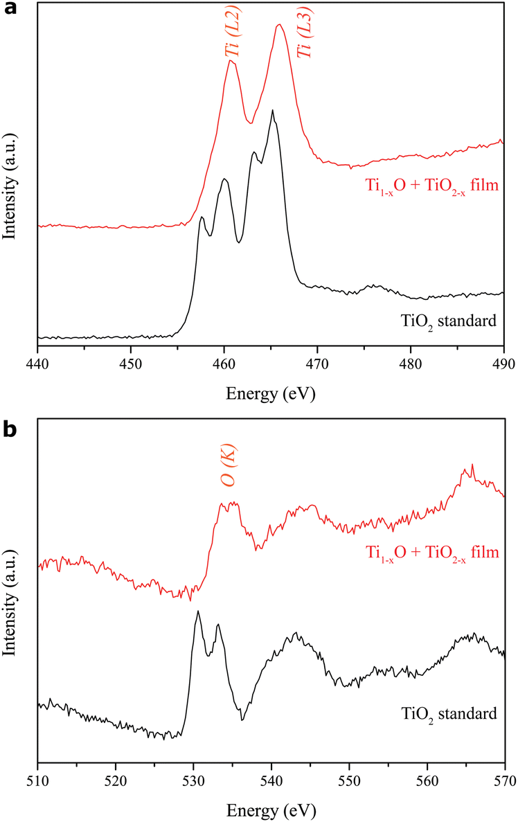
The background-subtracted Ti L2,3-edge and O K-edge EELS spectra of the thin film as deposited on the FTO-glass under 600 mJ per pulse in vacuum are shown as examples in Fig. 8a and b, respectively. Note that the L2,3 edge of 3d transition metals is generally dominated by the dipole-allowed transition of 2p electrons to 3d unoccupied states (L2: 2p1/2 → 3d3/2, L3: 2p3/2 → 3d5/2) and generally reflects the valence state of transition-metal atoms. The two major L3 and L2 edges of the predominant rock-salt Ti1−xO and rutile TiO2−x turned out not to be doublets (Fig. 8a). In contrast, the stoichiometric rutile TiO2 standard (EELS Atlas, Gatan Inc.) shows subdivided peaks due to strong crystal-field splitting of Ti4+ from octahedrally coordinated oxygens (Gloter et al., 2009; Huang et al., 2010).15,22 Apparently, the crystal field deteriorates due to the significant nonstoichiometry (x) in the present nanocondensates for imperfect octahedral oxygen coordination. This is also manifested by the EELS O–K edge in Fig. 8b, showing that the Ti 3d and O 2p hybridized peak is slightly split by 1.5 eV for the film in contrast with 2.75 eV for the stoichiometric rutile standard. It should be noted that the L2,3 and K edges of the film shift to high energies relative to the rutile standard, apparently owing to the presence of Ti2+/Ti3+ and defect clusters in the intimate intergrowth of rock-salt Ti1−xO and rutile TiO2−x.
 | ||
| Fig. 8 Electron energy loss spectra of (a) Ti L2,3 and (b) O K edge of the R-Ti1−xO + r-TiO2−x predominant thin film as deposited on the FTO-coated silica glass by the PLA process under 600 mJ per pulse in vacuum (red traces) in comparison with the rutile TiO2 standard (black traces, EELS Atlas, Gatan Inc.). | ||
Raman, PL, and UV-vis absorbance
Raman shifts showed up at ca. 264, 413, and 601 cm−1 for the predominant rock-salt Ti1−xO and rutile TiO2−x mixture in the films as deposited on the FTO-glass by PLA under various pulse energies (Fig. 9a). These shifts can be attributed to the multi- phonon process, Eg, and A1g modes of rutile TiO2−x, although with a significant shift of Eg and A1g bands towards higher wavenumber, i.e. lower frequency, compared with 445.8 and 609.8 cm−1, respectively, for stoichiometric rutile.23 This red shift effect is analogous to that due to Ti2O, Ti3O5, and some members of the homologous series TinO2n−1 (where n is a number between 4 and 10) phases produced by microwave plasma processing on titanium.24 In contrast, the Raman peak broadening and intensity reduction of Eg and A1g modes can be attributed to the combined effects of crystallite size miniaturization, amorphization, and three-dimensional phonon confinement.25 It should be noted that the intensity ratio of Raman bands was approximately the same among common TiO2, such as A1g/Eg of rutile and A1g/Eg or B1g/Eg of anatase.26 In contrast, there was an irregular ratio of A1g/Eg for the present rutile TiO2−x, which has an intimate mixture of rock-salt Ti1−xO with a paracrystalline distribution of defect clusters. The corresponding photoluminescence spectra of the films as compiled in Fig. 9b show significant violet and green emissions for the 200 mJ per pulse sample. These emissions can be attributed to the predominant rock-salt Ti1−xO and rutile TiO2−x, respectively, in view of the reported value for each phase. In fact, titanium monoxide thin films (presumably TiO with some extent of nonstoichiometry and protonation) were prepared from precursor TiCl3 in distilled water using thermal chemical spraying on thin glass bases heated to a temperature of 350 °C.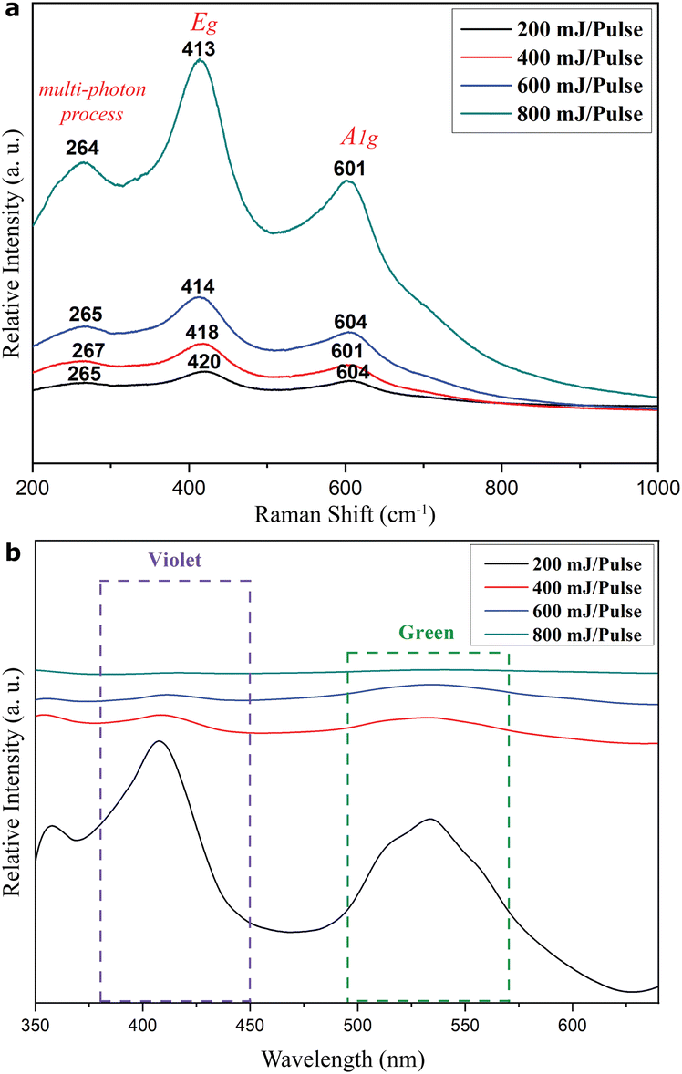 | ||
| Fig. 9 (a) Raman and (b) PL spectra of the R-Ti1−xO + r-TiO2−x predominant thin film as deposited on the FTO-coated silica glass by the PLA process in vacuum under specified laser pulse energies of 200, 400, 600 and 800 mJ per pulse, respectively. | ||
This was followed by annealing at 323, 373, 423, 473, and 523 K. These films showed PL emissions in the range of 310–470 nm (peaks at 367, 376, 402, 408, and 429 nm) with an excitation wavelength of 300 nm.27 These emission peaks were attributed to defect-trapped excitons which enhance various states in the TiO band gap and recombination center electrons.27 As for the sol–gel TiO2 thin film, it shows green and orange emissions depending on the post-deposition processing, i.e. annealing at 500 °C in air or vacuum and UV light curing at room temperature.28 It is noteworthy that violet and green emissions are rather broad and are progressively blurred as the pulse energy for film deposition increases from 400 to 800 mJ per pulse. This indicates that the recombination rate of photogenerated electrons and holes is suppressed for rock-salt Ti1−xO and rutile TiO2−x as the laser pulse energy increases. However, the green emission became stronger for all the films (fabricated by PLA under 200 to 800 mJ per pulse) after annealing at 450 °C in air for 5 h (Fig. S11†); apparently, this was due to the enhanced R → r transformation.
The UV–vis spectra of the films deposited on the FTO-silica glass under 200 to 800 mJ per pulse in vacuum are compared to corresponding rutile TiO2 targets in Fig. 10a. In contrast to the rutile TiO2−x, target which showed typical iron grayish color and UV absorption of around 200–400 nm, the films showed enhanced white light absorption, i.e. in the wavelength range of 400–800 nm in accordance with their darkish color as seen by the naked eye. The corresponding band gap from the Tauc plot (Fig. 10b) decreases from 1.7 to ca. 1.4 eV with an increase in pulse energy for both the films, and the ablated targets more or less with the accumulated condensates of R-Ti1−xO and r-TiO2−x for more effective visible absorption. The band gap widened significantly for the films but remained unchanged for the ablated targets after annealing at 450 °C in air for 5 h.
 | ||
| Fig. 10 (a) UV-vis absorbance spectra and (b) the corresponding band gap of the R-Ti1−xO + r-TiO2−x predominant thin film as deposited on the FTO-coated silica glass by the PLA process in vacuum under 200, 400, 600 and 800 mJ per pulse, respectively, vs. that subject to further annealing at 450 °C in air for 5 h. The control group is the ablated TiO2 rutile target without/with further 450 °C annealing in air for 5 h. | ||
Photoelectrochemical measurements
The current–voltage hysteresis curves related to the so-called current density (J)–V curve as measured by a potentiostat at room temperature (Fig. 11a) indicates that the darkish thin films with the predominant R-Ti1−xO and r-TiO2−x as deposited on FTO-glass under 200–800 mJ per pulse have about the same photoelectron transfer efficiency for redox catalytic performance in terms of fair visible absorption and carrier recombination. Such redox properties remained almost the same for the films after annealing at 450 °C in air for 5 h (not shown). In contrast, the current density–time curves of the darkish films (Fig. 11b) show good photocurrent density close to that of FTO29 and Ag: TiO2 thin films30 for potential photovoltaic applications. The film produced at 600 mJ per pulse turned out to be optimum with the highest current density, indicating that the film performance has little to do with the FTO underneath. Such photoelectronic properties were further improved for the films after annealing at 450 °C in air for 5 h (not shown). It should be noted that the titanium oxide thin film as deposited on silica glass (Fig. 1b) was retained upon ambient aging for more than 1 year, although the crystalline R + r phases became less than the amorphous phase (Fig. S12a†). As for a thin film subjected to immersion in KOH solution for more than 12 hours and PEC measurement under xenon lamp irradiation and an external voltage of 1.2 V, the amorphous phase was even more pronounced (Fig. S12b†). | ||
| Fig. 11 Cyclic voltammetry (a) and chopped current density–time curve (b) of a photoelectrochemical cell using the titanium oxide film/FTO as the working electrode in a three-electrode configuration with 1.2 V external bias under xenon illumination, indicating that a sample prepared with the optimum pulse energy (i.e. 600 mJ per pulse) has the highest current density. | ||
Discussion
Pulse-energy tailored lattice parameters and x of Ti1−xO and TiO2−x
The rock-salt Ti1−xO nanocondensates in the thin film deposited on silica glass free of FTO coating (Fig. 1b) showed progressively smaller X-ray lattice parameters down to ca. 0.418 nm as the pulse energy increased from 400 to 800 mJ per pulse. This compares with 0.4180 nm (JCPDS file 65-2900) or the even larger 0.4228 nm documented for stoichiometric TiO.4 In general, the lattice parameter increases with the decreasing extent of nonstoichiometry x for a transition metal monoxide such as wüstite (Fe1−xO) due to the so-called Jette and Foote rule,31 but decreases with an increasing extent of applied pressure such as by the PLA process to fabricate dense post-rutile phases of TiO2.10,11 For this reason, because R-Ti1−xO and r-TiO2−x nanoparticles are intimately mixed which interferes with chemical composition analysis, it is very difficult if not impossible to determine the exact x values for the two phases. Nevertheless, XRD and chemical analyses on high-pressure hot-pressed specimens showed that rutile has a significant extent of non-stoichiometry ranging from TiO1·86 to TiO1·91.32 In contrast, high-pressure experimental results at 300 °C indicated that the value of x in Fe1−xO decreases as the pressure is increased isothermally to 100 kbar, and later increases as the pressure increases above 100 kbar.33 It is not clear whether higher pulse energy favors the high entropy state of R-Ti1−xO by a larger extent of nonstoichiometry (x). In any case, an optimum x for each phase for fair lattice match at (hkl)R-specific surfaces is of concern for the transformation twinning path, as addressed in the following section.R-Ti1−xO to r-TiO2−x transformation (I): the dense (hkl)-specific transformation path
The rock-salt-type Ti1−xO nanocondensates, as deposited on the FTO-silica substrate, were partially transformed into rutile-type TiO2−x (Fig. 6) rather than into the structurally more similar anatase. This can be rationalized by the dense (111)R-specific phase transformation path under the influence of directional (monotonous outward) oxygen supply from FTO and silica glass at rather high temperatures in the rutile T–P stability field during the PLA deposition process in vacuum. Apparently, without FTO coating, the amorphous silica substrate was still effective at oxidizing Ti1−xO into titanium double oxide (Fig. 1b) in accordance with the optically birefringent rutile TiO2−x particulates as identified by optical polarized microscopy (ESI† C). The Ti inward and Sn outward diffusion were restricted to a narrow (ca. 50 nm thick) interdiffusion zone (Fig. 3), and hence played a minor/negligible role in the phase selection in the film overlain on FTO. Conversely, the predominant {111}R surface of the R-Ti1−xO nanocondensates with such a preferred orientation on the substrate enabled the topotaxial nucleation of r-TiO2−x with the preferred (101)r orientation (cf. XRD results in Fig. 1b), as otherwise anatase would be favored on the {100}R surface by the excellent parallel-lattice along the a1 and a2 axes of anatase (Kao et al., 2011)17 (in this connection, thermal oxidation of Ti film in air is known to produce oxygen-enriched Ti, i.e. an intermediate hexagonal Ti2O phase which transforms into rutile at 700 °C (Ting et al., 2000)34 with (200) texture due to the (0002) preferred orientation of Ti2O after Ti film (Ting et al., 2022)).35 There are two reasons for having (101)r preferred orientations of the present r-TiO2−x condensates by the PLA process. First, the (101)r surface has the second lowest surface energy among the habit planes of rutile, i.e. γ{110} < {101} < {221} < {100} with surface energies of 1.78, 1.85, 2.02, and 2.08 J m−2, respectively, according to the atomistic simulations in Oliver et al. (1997).36 Second, the (101)r surface has higher oxygen atom coverage and surface density than {110}r or (100)r, and both have edge-shared TiO6 octahedral chains along the c-axis, for easier oxidation and densification under the PLA process, analogous to the formation of dense (hkl) surfaces for α-PbO2-type TiO2 (Chen and Shen, 2002).10Regarding the temperature and pressure effects on phase stability, TiO film was found to partially transform into anatase upon thermal oxidation in air at 400 °C, i.e. in the anatase stability field below the anatase/rutile equilibrium temperature of 600 °C at 1 atm; see Fig. 2 in Jamieson and Olinger (1969).37 In addition, uniform anatase-type TiO2 nanoparticles were synthesized by the gel–sol process from a condensed Ti(OH)4 gel upon aging at 140 °C under optimum pH.5 Confined pressure by the very rapid heating and cooling effect of the PLA process would also favor rutile formation rather than anatase in view of the T–P phase diagram of TiO2.37 It is interesting that the anatase-to-rutile phase transformation was found to nucleate at anatase {112} twin boundaries formed by oriented attachment of nanocrystalline anatase during hydrothermal synthesis at 250 °C.6 This implies that the rock-salt Ti1−xO {111} twin boundary of the primary butterfly twin boundary as formed by a condensation-coalescence mechanism in the PLA process would also act as a nucleation site for rutile to form a secondary butterfly twin in terms of lattice match with a fair 2-D CSL, as addressed in the following.
R-Ti1−xO to r-TiO2−x transformation (II): 2-D CSL at phase interface and twin boundary
Given the COR [101]R//[11]r with (11)R//(011)r as the phase interface (see the trace in the stereographic projection in Fig. S13†) and twin boundary of each counterpart, the geometry and energetics of such a special interface can be visualized by the following construction of the coincidence site lattice (CSL) with in situ constrained lattice parameters based on the XRD d-spacing of (111)R and (101)r for the case of 600 mJ per pulse (Fig. 1b). As shown by the schematic drawing of atom disposition in Fig. 12, the (11)R//(011)r interface in the top view is about the match of cation-anion unmixed (111)R and (011)r planes to have a fair 2-D rectangular (or twinned primitive rhombohedra) CSL in terms of the periodic match of Ti atoms. The unconstrained misfits for CSL are calculated from the XRD d-spacings of R-Ti1−xO (d111R = 0.241 nm; d211R = 0.171 nm, JCPDS file 65-2900) and r-TiO2−x (d101r = 0.249 nm; d122r = 0.120 nm, JCPDS file 21-1276) as, ε0 = (d011r − d111R)/d111R = 0.033 for the quasi close-packed plane match| ε1 = ε〈111〉r//〈110〉R = 0.21 |
| ε2 = ε〈755〉r//〈112〉R = 0.37 |
 | ||
| Fig. 12 Schematic drawing of the (11)R//(011)r interface in top view with Ti (open circle) and O (solid circle) atoms denoted in black and red for R and r, respectively with CSL in terms of the periodic match of Ti atoms outlined by blue dashed lines. | ||
The (11)R/(011)r pole pair is the only low-index plane match to act as a habit plane for the composite (cf. Fig. S13†). The anisotropic stress state in terms of εo, ε1, and ε2 then exerts significant shear stress along the habit (11)R//(011)r interface with a fair CSL (Fig. 12). This accounts for the extensive faulting and even secondary deformation twinning for relic R-Ti1−xO upon transformation into r-TiO2−x (Fig. 6), presumably coupled with the synchro-shear of the quasi-close-packed (11)R and (011)r atom planes to form super-partial dislocations. In this connection, the rutile nanocondensates that underwent the (011)-specific coalescence process were found to relax by shearing along 〈011〉 directions to form stacking faults.14 It is also interesting that there is an interaction of dislocations belonging to the slip systems {101}〈01〉 and {110}〈001〉 with small and extended nonstoichiometric defects.38
Topologically, there is a similar geniculate structure unit at the (11)R twin boundary ([101](11) 70.5° tilt boundary) and (011)r twin boundary (i.e. [11](011) 135.0° tilt boundary equivalent to [100](011) 114.4° tilt boundary39) presumably with O or Ti atoms merged from neighboring layers (Fig. S14a†). This accounts for the favorable nucleation of r-TiO2−x at the R-Ti1−xO twin boundary. The 2-D lattice match at the (11)R//(011)r interface allows the topotaxial nucleation of three twinned variants of r-TiO2 from the R-Ti1−xO host, involving considerable TiO6 rotation at the coincidence site (Fig. S14b†) to introduce deformation twinning and faulting (Fig. S10†). Thus, the R-Ti1−xO coalescence twin variants in the film fabricated optimally at 600 mJ per pulse (Fig. S6†) may develop into r-TiO2−x multiple twin variants upon thermal oxidation analogous to that via a hydrothermal reaction.39 (Regarding the (hkl)-specific coalescence twinning, it was originally reported for CeO2 condensates by the PLA process40 and later observed for rock-salt-type magnesiowüstite nanocondensates with (111) twin boundaries.41) The topological constraint at such a (111)R coalescence twin boundary with close-packed atoms accounts for the favorable dense-phase selection of rutile rather than anatase and polysynthetic deformation/closure twins that accompanied the partial R → r transformation for strain relaxation (Fig. S10†).
It is interesting that the dense α-PbO2-type TiO2 (denoted α) nucleated at the rutile (011)r twin boundary by the COR [110]α//[11]r; (001)α//(011)r in the UHP metamorphic terrain12 did not form a twinned bicrystal because the (001)α plane happens to be a mirror plane given space group Pbcn (Fig. S15†). For the same reason, a rutile twinned bicrystal cannot be formed by nucleation at the (112) twin boundary of anatase (A) following the COR (112)A//(010)r; [01]A//[6]r because (010)r as a match plane at the interface (cf.Fig. 6 in Penn and Banfield, 1999),6 is again a mirror plane given space group P42/mnm. Indeed, such rutile nuclei on the (112)A anatase twin surface are a single crystal, as indicated by the lattice fringes (cf.Fig. 4 in Penn and Banfield).6 Thus, the geniculate twinned bicrystal of single-phase rutile with (011)r twin boundary via the hydrothermal process, as shown in Fig. 5 of Penn and Banfield,6 or via the PLA process in vacuum with purged oxygen,14 were most likely formed by the crystallites coalescencing over an atomic plane which happens to be a non-mirror plane, i.e. (011)r for the (hkl)-specific impingement. The criterion of the novel secondary butterfly-transformation twinning in this work, along with other twinning mechanisms under natural or synthetic conditions, are compiled schematically in Fig. S15.†
Point defects in Ti1−xO and TiO2−x for defect clustering and charge transfer
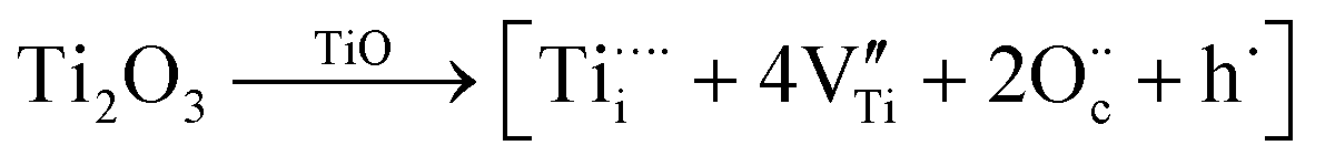
The side-band diffractions in the [001] zone axis of a single rock-salt Ti1−xO nanocondensate (Fig. 5a and b) can be attributed to the paracrystalline state of the defect clusters. In this regard, rock-salt-type 3d transition metal monoxides with a considerable extent of nonstoichiometry, such as Fe1−xO (x ≤ 0.15),42 Co1−xO (x ∼ 0.01 extended to Co3−xO4),43 Ni1−xO doped with Zr4+,44 and even an NiO–CaO binary,45 tend to have their defect clusters in a paracrystalline distribution, which is why the spacing between defects remains fairly constant, but the relative lateral translation may occur with more variation.46,47 The present rock-salt Ti1−xO paracrystal is likely to have about 4 octahedral cation vacant sites surrounding one Ti4+-filled tetrahedral interstitial site, analogous to the 4:1 type defect clusters in Fe1−xO.42 From a defect chemistry viewpoint, rock-salt Ti1−xO doped with aliovalent Ti4+/Ti3+, as indicated by XPS (Fig. 6), and extra O2− in the lattice ( ) by directional oxygen uptake from FTO or an available proton (h˙) would undergo following equations for paracrystal formation:
 | (1) |
 | (2) |
 may in fact be tetravalent Ti in association with a pair of free electrons for a paracrystal with Ti4+ dopant in eqn (1). Alternatively, a hydrogen dopant, i.e. an electron–hole h˙ may be involved in the case of a Ti3+ dopant in eqn (2) to form a paracrystalline assembly. The concentration of the above defect clusters in the paracrystal can be scaled by their interspacing, which is ca. 2.5 times the unit cell dimension of the present R-Ti1−xO (Fig. 5b).
As for the rutile TiO2−x condensates, the Ti4+ ion could be replaced by larger-size Ti2+ or Ti3+ to introduce  charge/volume compensation in view of the fact that TiO2−x is a typical oxygen-deficient oxides48 and is known to contain Ti4+ interstitials and oxygen vacancies with low formation energy.49 The type of defect clusters for rutile TiO2−x are then likely to be [
 ] or [
 ], which did not assemble as a paracrystal but could cause stacking faults, as shown in Fig. 6. The intimate mixture of such defective rock-salt Ti1−xO and rutile TiO2−x would then have various point-defect species with multiple valences to facilitate charge transfer. The Ti2+ ion may be oxidized as Ti3+ and Ti4+ at the film surface accompanied by inward electron migration to oxygen vacancies as VO2−, in view of such species being revealed by the XPS spectra for a film fabricated at the optimum pulse energy of 600 mJ per pulse (Fig. 7a and b). It would hence affect the photocatalytic and photoelectrochemical properties.
Defect-dependent photocatalytic and photoelectrochemical properties
The R-Ti1−xO + r-TiO2−x films overlain on the FTO-glass film under 200–800 mJ per pulse remained darkish by white light absorbance. Meanwhile, their green PL emissions were enhanced at the expense of violet emission by the R → r transformation, whereas the band gap became wider, and the periodic on–off optocurrent density improved after the films were annealed at 450 °C in air for 5 h. This allows potential photovoltaic, photocatalytic, and optoelectronic applications of the R-Ti1−xO + r-TiO2−x nanocondensates in harsh environments, such as deserts, the earth's interior (mining tunnels), polluting factories, or space shuttles/stations in outer space.In fact, the R-Ti1−xO + r-TiO2−x nanocondensates have abundant x-enabled oxygen/cation vacancies and defect clusters, which affect the efficiency of charge carrier trapping, migration, transfer, and separation. The recombination of such charge carriers below a certain concentration level to avoid the so-called fluorescence quenching effect at temperature and pressure would enhance the green PL intensities of rutile TiO2−x at the expense of the UV intensity of rock-salt Ti1−xO upon annealing at different temperatures in air (cf.Fig. 9b and S8†) although the actual PL mechanisms of Ti1−xO and TiO2 are yet to be clarified.50 (The rutile PL may involve self-trapped holes located at oxygen atoms or trapped electrons occupying midgap states positioned below the Fermi level, according to Pallotti et al., 2017.50) In any case, the enhanced green PL emission at the expense of UV emission upon thermal oxidation for an R → r transformation would have potential application as multiple sensors of temperature and oxygen fugacity.
In contrast, a lower recombination rate of electrons and holes is beneficial to higher photoconductivity and photoelectrochemical activity, as measured by the potentiostat in this study (Fig. 11). In this regard, formation energies for the point-defect species in rutile with alleged TiO2 stoichiometry were calculated by the polarizable point-ion shell mode to be 10.8 eV for interstitial Ti4+, 10.1 eV for an oxygen vacancy with 2+ effective charge, and 2.9 eV for Ti4+ migration along the crystallographic c axis.49 The formation energies for the point-defect species in rock-salt Ti1−xO would be different from those of rutile TiO2−x in view of the crystal field splitting in: (I) TiO2via EELS showing strong splitting for L3 and L2 edges due to Ti4+ from the octahedrally coordinated oxygens,15,22 (II) Ti3O5via EPR spectroscopy regarding Ti3+ ions in the mixed-valence phases of the titanium-oxygen system TinO2n−1 (ref. 51) and (III) the stability of oxygen vacancies at the subsurface of TiO2 (with anatase as an analog) in terms of the Ti-3d orbitals in different crystal fields occupied by excess electrons.52 Such various energy states under the crystal field effect for the point-defect species in the intimate mixture of R-Ti1−xO + r-TiO2−x nanocondensates could then possess photoelectronic characteristics, such as double UV-green PL emissions, to act as multiple sensors.
Conclusions
By the PLA of a rutile polycrystal in vacuum for film deposition on an FTO-coated or FTO-free silica glass substrate, we were able to produce rock-salt Ti1−xO and rutile TiO2−x nanocondensates with a shape-preferred orientation adopted by the close-packed planes. The novel R → r transformation was identified to follow optimum COR [101]R//[11]r; (11)R//(011)r for composite butterfly twins due to topotaxial nucleation of rutile at the (111)R surface or coalescence twin boundary to form a (11)R//(011)r interface with a fair CSL in terms of the periodic match of Ti atoms. Still, there is a significant anisotropic stress state at the transformation front, leaving secondary deformation twins, stacking faults, and dislocations in terms of the close-packed planes for both phases. The dense (111)R-specific R → r transformation is in drastic contrast to previous observations of the (100)-mediated TiO → anatase transformation by thermal oxidation of Ti in air or the reverse anatase to TiO transformation by in situ heating in TEM. The composite butterfly twin from R → r transformation also sheds light on the underlying criterion of the secondary butterfly twin being the (011)r match plane, which happens to be a non-mirror plane.
The intimately mixed R-Ti1−xO and r-TiO2−x nanocondensates have buffered x and oxygen for crystal-field and surface-directed charge transfer in terms of planar/point defects and paracrystalline distribution of defect clusters. This accounts for characteristic violet/green double PL emissions, white-light absorbance, and fine photoelectrochemical properties for potential photocatalytic and optoelectronic applications, in particular as multiple sensors in terms of the R → r transformation and even excellent electron conductivity when x in R-Ti1−xO approaches zero.
Author contributions
Conceptualization, C.-N. H. and P. S.; methodology, C.-N. H., J.-Y. C. and P. S.; validation, C.-N. H., Y.-X. Lin and P. S.; formal analysis, C.-N. H. and J.-Y. C.; investigation, C.-N. H., J.-Y. C. and P. S.; resources, C.-N. H. and J.-Y. C.; writing– original draft preparation, C.-N. H. and J.-Y. C.; writing – review and editing, C.-N. H. and P. S.; supervision C.-N. H. and P. S.; project administration, C.-N. H. All authors have read and agreed to the published version of the manuscript.Conflicts of interest
There are no conflicts to declare.Acknowledgements
The authors gratefully acknowledge anonymous reviewers for their positive feedback, their relevant and constructive comments on our manuscript, and Ms. Shih-Wen Tseng for the use of JEOL JEM-2100F Cs STEM belonging to the Instrument Center of National Cheng Kung University. This work was supported by the National Science and Technology Council, Taiwan, ROC under contract MOST 110-2637-E-218-007 and NSC 92-2120-M-110-001.References
- N. S. Gunda, B. Puchala and A. Van der Ven, Phys. Rev. Mater., 2018, 2, 033604 CrossRef CAS.
- X. Chen, L. Liu, P. Y. Yu and S. S. Mao, Science, 2011, 331, 746–750 CrossRef CAS PubMed.
- F. Li, Y. Zou, M.-G. Han, K. Foyevtsova, H. Shin, S. Lee, C. Liu, K. Shin, S. D. Albright, R. Sutarto, R. Sutarto, F. He, B. A. Davidson, F. J. Walker, C. H. Ahn, Y. Zhu, Z. G. Cheng, I. Elfimov, G. A. Sawatzky and K. Zou, Sci. Adv., 2021, 7, eabd4248 CrossRef CAS PubMed.
- D. Wang, C. Huang, J. He, X. Che, H. Zhang and F. Huang, ACS Omega, 2017, 2, 1036–1039 CrossRef CAS PubMed.
- T. Sugimoto, X. Zhou and A. Muramatsu, J. Colloid Interface Sci., 2003, 259, 43–52 CrossRef CAS PubMed.
- R. L. Penn and J. F. Banfield, Am. Mineral., 1999, 84, 871–876 CrossRef CAS.
- Y. Zhang, C. Guerra-Nuñez, I. Utke, J. Michler, P. Agrawal, M. D. Rossell and R. Erni, Chem. Mater., 2017, 29, 2232–2238 CrossRef CAS PubMed.
- M. B. Cosar, K. C. Icli and M. Ozenbas, J. Vac. Sci. Technol., A, 2019, 37, 031505 CrossRef.
- R. van de Krol and M. Grätzel, Photoelectrochemical Hydrogen Production, Springer, New York, NY, 2012 Search PubMed.
- S. Y. Chen and P. Shen, Phys. Rev. Lett., 2002, 89, 096106 CrossRef PubMed.
- S. Y. Chen and P. Shen, Jpn. J. Appl. Phys., 2004, 43, 1519 CrossRef CAS.
- S.-L. Hwang, P. Shen, H.-T. Chu and T.-F. Yui, Science, 2000, 288, 321–324 CrossRef CAS PubMed.
- M.-H. Tsai, S.-Y. Chen and P. Shen, J. Aerosol Sci., 2005, 36, 13–25 CrossRef CAS.
- M.-H. Tsai, S.-Y. Chen and P. Shen, Nano Lett., 2004, 4, 1197–1201 CrossRef CAS.
- C.-N. Huang, J.-S. Bow, Y. Zheng, S.-Y. Chen, N. Ho and P. Shen, Nanoscale Res. Lett., 2010, 5(6), 972 CrossRef CAS PubMed.
- C.-H. Wu, S.-Y. Chen and P. Shen, CrystEngComm, 2014, 16, 2220–2229 RSC.
- C.-H. Kao, S.-W. Yeh, H.-L. Huang, D. Gan and P. Shen, J. Phys. Chem. C, 2011, 115, 5648–5656 CrossRef CAS.
- X. Chen, S. N. Hosseini and M. A. van Huis, ACS Appl. Nano Mater., 2022, 5, 1600–1606 CrossRef CAS PubMed.
- S. Amano, D. Bogdanovski, H. Yamane, M. Terauchi and R. Dronskowski, Angew. Chem., Int. Ed., 2016, 55, 1652–1657 CrossRef CAS PubMed.
- R. D. Shannon, Acta Crystallogr., Sect. A: Cryst. Phys., Diffr., Theor. Gen. Crystallogr., 1976, 32, 751–767 CrossRef.
- W. H. Lee and P. Shen, J. Solid State Chem., 2002, 166, 197–202 CrossRef CAS.
- A. Gloter, C. Ewels, P. Umek, D. Arcon and C. Colliex, Phys. Rev. B: Condens. Matter Mater. Phys., 2009, 80, 035413 CrossRef.
- H. L. Ma, J. Y. Yang, Y. Dai, Y. B. Zhang, B. Lu and G. H. Ma, Appl. Surf. Sci., 2007, 253, 7497–7500 CrossRef CAS.
- E. J. Ekoi, A. Gowen, R. Dorrepaal and D. P. Dowling, Results Phys., 2019, 12, 1574–1585 CrossRef.
- V. Swamy, B. C. Muddle and Q. Dai, Appl. Phys. Lett., 2006, 89, 163118 CrossRef.
- J. Yan, G. Wu, N. Guan, L. Li, Z. Li and X. Cao, Phys. Chem. Chem. Phys., 2013, 15, 10978–10988 RSC.
- M. L. Hussein and G. A. Kadhim, NeuroQuantology, 2021, 19, 32–37 CrossRef.
- S. Mondal and D. Basak, J. Lumin., 2016, 179, 480–486 CrossRef CAS.
- S.-T. Zhang, Study of fluorine-doped tin oxide (FTO) thin films for photovoltaics applications, Ph. D. Thesis, Communauté Université Grenoble Alpes (UGA) and Technische Universität Darmstadt (TU Darmstadt) 2017 Search PubMed.
- S. Katsiaounis, J. Panidi, I. Koutselas and E. Topoglidis, Coatings, 2020, 10, 130 CrossRef CAS.
- E. R. Jette and F. Foote, J. Chem. Phys., 1933, 1, 29–36 CrossRef CAS.
- F. W. Vahldiek, J. Less-Common Met., 1968, 14, 133–143 CrossRef CAS.
- P. Shen, W. A. Bassett and L.-G. Liu, Geochim. Cosmochim. Acta, 1983, 47, 773–778 CrossRef CAS.
- C.-C. Ting, S.-Y. Chen and D.-M. Liu, J. Appl. Phys., 2000, 88, 4628–4633 CrossRef CAS.
- C.-C. Ting, S.-Y. Chen and D.-M. Liu, Thin Solid Films, 2002, 402, 290–295 CrossRef CAS.
- P. M. Oliver, G. W. Watson, E. T. Kelsey and S. C. Parker, J. Mater. Chem., 1997, 7, 563–568 RSC.
- J. C. Jamieson and B. Olinger, Am. Mineral., 1969, 54, 1477–1481 Search PubMed.
- M. G. Blanchin, L. A. Bursill, C. Lafage and P. B. Hirsch, Proc. Math. Phys. Eng. Sci., 1990, 429, 175–202 CAS.
- V. Jordan, U. Javornik, J. Plavec, A. Podgornik and A. Rečnik, Sci. Rep., 2016, 6, 24216 CrossRef CAS PubMed.
- W.-H. Lee and P. Shen, J. Cryst. Growth, 1999, 205, 169–176 CrossRef CAS.
- T.-Y. Lin, S.-S. Lin, S.-Y. Chen and P. Shen, CrystEngComm, 2015, 17, 3468–3477 RSC.
- C. R. A. Catlow and B. E. F. Fender, J. Phys. C: Solid State Phys., 1975, 8, 3267 CrossRef CAS.
- W.-H. Lee and P. Shen, J. Solid State Chem., 2004, 177, 101–108 CrossRef CAS.
- J. Chen and P. Shen, J. Solid State Chem., 1998, 140, 361–370 CrossRef CAS.
- M.-L. Jeng and P. Shen, J. Solid State Chem., 2000, 152, 421–427 CrossRef CAS.
- T. R. Welberry and A. G. Christy, J. Solid State Chem., 1995, 117, 398–406 CrossRef CAS.
- T. R. Welberry and A. G. Christy, Phys. Chem. Miner., 1997, 24, 24–38 CrossRef CAS.
- O. T. Sørensen, Nonstoichiometric Oxides, Academic Press, 1981 Search PubMed.
- H. Sawatari, E. Iguchi and R. J. D. Tilley, J. Phys. Chem. Solids, 1982, 43, 1147–1155 CrossRef CAS.
- D. K. Pallotti, L. Passoni, P. Maddalena, F. Di Fonzo and S. Lettieri, J. Phys. Chem. C, 2017, 121, 9011–9021 CrossRef CAS.
- J. F. Houlihan, D. P. Madacsi and L. N. Mulay, Mater. Res. Bull., 1976, 11, 307–313 CrossRef CAS.
- W. Yin, B. Wen, Q. Ge, X. Wei, G. Teobaldi and L. Liu, Prog. Nat. Sci.: Mater. Int., 2020, 30, 128–133 CrossRef CAS.
Footnote |
| † Electronic supplementary information (ESI) available. See DOI: https://doi.org/10.1039/d3ce01091k |
| This journal is © The Royal Society of Chemistry 2024 |