
Effect of grain coalescence on dislocation and stress in GaN films grown on nanoscale patterned sapphire substrates
Zuojian
Pan
 a,
Zhizhong
Chen
*abc,
Yiyong
Chen
a,
Haodong
Zhang
a,
Han
Yang
a,
Ling
Hu
a,
Xiangning
Kang
a,
Ye
Yuan
d,
Chuanyu
Jia
e,
Zhiwen
Liang
b,
Qi
Wang
b,
Guoyi
Zhang
ab and
Bo
Shen
ac
a,
Zhizhong
Chen
*abc,
Yiyong
Chen
a,
Haodong
Zhang
a,
Han
Yang
a,
Ling
Hu
a,
Xiangning
Kang
a,
Ye
Yuan
d,
Chuanyu
Jia
e,
Zhiwen
Liang
b,
Qi
Wang
b,
Guoyi
Zhang
ab and
Bo
Shen
ac
aState Key Laboratory for Artificial Microstructure and Mesoscopic Physics, School of Physics, Peking University, Beijing 100871, China. E-mail: zzchen@pku.edu.cn
bDongguan Institute of Optoelectronics, Peking University, Dongguan, Guangdong 523808, China
cYangtze Delta Institute of Optoelectronics, Peking University, Nantong, Jiangsu 226000, China
dSongshan Lake Materials Laboratory, Dongguan, Guangdong 523808, China
eSchool of Electrical Engineering and Intelligentization, Dongguan University of Technology, Dongguan, Guangdong 523808, China
First published on 21st December 2023
Abstract
High-quality GaN films on nanoscale patterned sapphire substrates (NPSSs) are required for micro-light-emitting diode (micro-LED) display. In this study, two types of nucleation layers (NLs), including in situ low-temperature grown GaN (LT-GaN) and ex situ physical vapour deposition AlN (PVD-AlN), are applied on cone-shaped NPSS. The coalescence process of GaN grains on the NPSS is modulated by adjusting the three-dimensional (3D) growth temperatures. Results show that low 3D temperatures help to suppress the Ostwald ripening of GaN grains on the NPSS, facilitating the uniform distribution of 3D GaN grains. Higher 3D temperatures lead to a decrease in the edge dislocation density, accompanied by an increase in residual compressive stress. Compared with LT-GaN NLs, PVD-AlN NLs can effectively improve the growth uniformity, suppress the tilting and twisting of GaN grains grown on NPSSs, and promote the orientation consistency of crystal facets during coalescence. The GaN films grown on NPSSs with PVD-AlN NLs exhibit a decrease in the coalescence time from 2000 s to 500 s, a reduction in dislocation densities from 2.8 × 108 cm−2 to 1.4 × 108 cm−2, and an increase in the residual compressive stress from 0.98 GPa to 1.41 GPa compared to those grown on LT-GaN NLs. This study elucidates trends in dislocation and stress evolution in GaN films on NPSSs with analysis of grain coalescence.
Introduction
In response to the growing demand for high-definition display technology, light-emitting diodes (LEDs) are constantly developing in the direction of miniaturization.1–3 For display technologies like virtual reality (VR) and augmented reality (AR), micro-LEDs with chip sizes smaller than 5 μm are typically necessary.4,5 However, the currently commercial microscale patterned sapphire substrates (MPSSs) exhibit pattern periods of approximately 3 μm, which already approach the chip sizes of micro-LEDs. The MPSS can cause inhomogeneous light emission for ultra-small micro-LEDs, considering the rough interface after stripping the MPSS in the micro-LED chip process. Nanoscale patterned sapphire substrates (NPSSs) have emerged as a crucial requirement for ultra-small micro-LED display technologies owing to their advantages in growth uniformity, light output efficiency, and crystal quality.6–9Defects and stress control of GaN films on NPSSs are critical factors affecting the non-radiative recombination and polarization electric field of micro-LEDs.10,11 Importantly, the nucleation and coalescence process of GaN grains in the initial growth stages directly affect the crystal quality and stress distribution of GaN films on NPSSs. Some studies have focused on the growth mechanism of GaN films on NPSSs when using low-temperature grown GaN (LT-GaN) nucleation layers (NLs).12,13 In recent years, physical vapour deposition AlN (PVD-AlN) has been developed to substitute LT-GaN as NLs to acquire high-quality GaN films.14–17 High crystal quality GaN films grown on MPSSs with PVD-AlN NLs have been widely reported.16,18–23 A drastic reduction in dislocations at the top of the cone-shaped pattern was observed when using PVD-AlN NLs compared to LT-GaN NLs.16,18,19 Nevertheless, as the pattern period decreases from micrometres to nanometres, the spatial limitation effect on Ga adatom diffusion and desorption by nanopatterns of the NPSS changes. Thus, further studies are required regarding the growth kinetics of GaN on NPSS with PVD-AlN NLs.
The grain coalescence significantly influences the dislocation formation and stress evolution in GaN films on NPSS.13,24–26 During coalescence, tilting and twisting of GaN grains lead to screw and edge dislocation formation at the coalescence boundaries.26–28 Meanwhile, grain coalescence introduces tensile stress in GaN films.24,25 Notably, the density of GaN grain coalescence at the top of the cone-shaped pattern of the NPSS increases by one to two orders of magnitude compared to that of the MPSS, which poses challenges in controlling dislocations at the coalescence boundaries.29,30 Nonetheless, recent research has revealed that precisely controlling grain orientation by nanopatterned substrates can almost eliminate dislocations in AlN films at the coalescence boundaries.31 Accordingly, further investigations focusing on the coalescence of GaN grains on NPSSs are required to realize high-quality GaN films.
In this paper, the coalescence process of GaN grains on NPSSs with LT-GaN NLs and PVD-AlN NLs was studied in detail. Before grain coalescence, the grain density and size of three-dimensional (3D) GaN were modulated by adjusting 3D temperatures. The surface morphology and orientation characteristics of 3D GaN grains on the NPSS with LT-GaN NLs and PVD-AlN NLs were comparably investigated. After completion of the GaN film growth, dislocation densities and stress states were evaluated for GaN films undergoing different grain coalescence processes. Furthermore, microscopic measurements were conducted to explore dislocations and stress distributions at the coalescence boundaries. Finally, the GaN grain coalescence mechanism and its effect on dislocation formation and stress evolution were discussed and conclusions were drawn.
Experimental
2-inch cone-shaped NPSSs were fabricated by nano-imprint lithography (NIL) and inductively coupled plasma (ICP) dry etching using c-plane sapphire substrates. The pattern period, bottom diameter, and height were 535, 400, and 300 nm, respectively. The GaN films were grown on the prepared NPSS in an Aixtron Crius I 31 × 2 inch close-coupled showerhead metal–organic chemical vapour deposition (MOCVD) system. Trimethylgallium (TMGa) and ammonia (NH3) were used as group III and V precursors. Hydrogen (H2) was used as the carrier gas. As shown in Fig. 1(a) and (b), for sample A, conventional in situ 30 nm-thick LT-GaN NLs were grown at 540 °C on the NPSS in MOCVD. For sample B, ex situ 30 nm-thick PVD-AlN NLs were deposited on the NPSS by reaction magneto-sputtering technique. After that, 3D GaN layers were grown on both LT-GaN and PVD-AlN NLs with different 3D temperatures. Four sets of 3D temperatures (920 °C, 960 °C, 1000 °C, 1040 °C) were applied for samples A1–A4 and samples B1–B4, respectively. Benefiting from the short coalescence process of GaN grains grown on NPSS,32 the 3D growth time of all the samples was set to 300 s, which is sufficient for GaN grains to grow beyond cone height. Upon completion of the growth of the 3D GaN layers, GaN recovery layers were introduced to promote lateral coalescence. During the growth of the recovery layers, the growth temperatures, pressures, and V/III mole ratios transitioned slowly from the values of the 3D process to those of the two-dimensional (2D) process. Finally, the samples were finished with 2 μm-thick 2D GaN layers deposited at 1060 °C. The growth pressures of the 3D layers and 2D layers were 550 and 150 mbar. The V/III mole ratios of the 3D layers and 2D layers were 450 and 1022, respectively.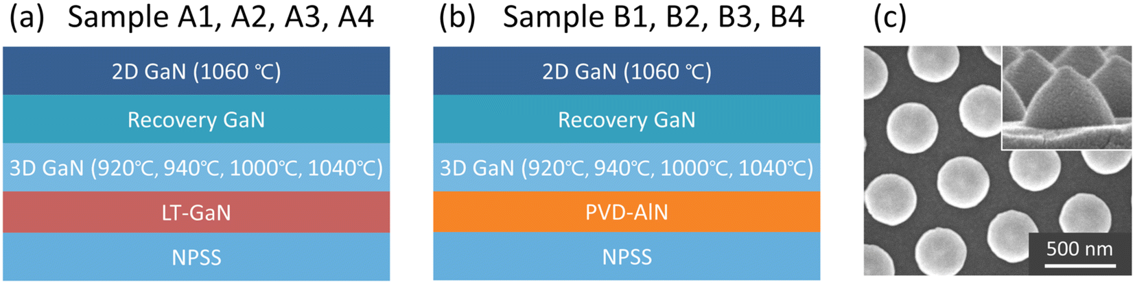 | ||
| Fig. 1 Schematic diagrams of GaN films grown on NPSS with (a) in situ LT-GaN NLs (samples A1–A4) and (b) ex situ PVD-AlN NLs (samples B1–B4). The order from 1 to 4 represents a gradual increase in 3D temperature. (c) A plane-view SEM image of NPSS; the inset shows a cross-sectional SEM image of the NPSS. | ||
The features of 3D growth GaN islands were recorded using scanning electron microscopy (SEM) (FEI Nova NanoSEM 430). The nanoscale surface morphologies of 3D GaN grains were further characterized using atomic force microscopy (AFM) (Bruker Dimension Icon). Ultra-fine AFM probes (Bruker FIB3D2-100A) with a high aspect ratio were utilized to obtain the exact morphology of the GaN grains. Besides this, the crystal quality of GaN films was measured using an X-ray diffraction (XRD) instrument (PANalytical X'Pert3 MRD, Bruker D8) operating at 40 kV and 40 mA. The ω-scan and φ-scan of the (12![[3 with combining macron]](https://www.rsc.org/images/entities/char_0033_0304.gif) 1) reflection were done using the Bruker D8 instrument to avoid monochromator error. Transmission electron microscopy (TEM) (FEI Tecnai F20) was applied to study the mechanisms of dislocation formation and evolution. Then, the residual stress of GaN epilayers was characterized by Raman scattering spectra (Horiba HR Evolution) with 0.5 cm−1 spectral resolution. In addition, the stress distribution of GaN films was measured by Raman mapping (Witec Alpha300 R) with a spatial resolution of 300 nm.
1) reflection were done using the Bruker D8 instrument to avoid monochromator error. Transmission electron microscopy (TEM) (FEI Tecnai F20) was applied to study the mechanisms of dislocation formation and evolution. Then, the residual stress of GaN epilayers was characterized by Raman scattering spectra (Horiba HR Evolution) with 0.5 cm−1 spectral resolution. In addition, the stress distribution of GaN films was measured by Raman mapping (Witec Alpha300 R) with a spatial resolution of 300 nm.
Results and discussion
Initial growth process of GaN on NPSS
The distribution of 3D GaN islands could be affected by surface diffusion and desorption of adatoms. The growth temperatures, pressures, and V/III mole ratios will affect the surface diffusion and desorption of Ga adatoms during the 3D process.33,34 At relatively high temperatures, the surface diffusion and desorption rates of Ga adatoms are greatly increased.33,34 In this work, various 3D temperatures (920 °C, 960 °C, 1000 °C, 1040 °C) were applied to explore the coalescence process of GaN islands grown on NPSS. The distribution of 3D GaN islands on NPSS with LT-GaN and PVD-AlN NLs was analysed using SEM and AFM. From the SEM and AFM images in Fig. 2 and 3, 3D GaN islands arise from the trenches between the patterns and coalesce with the surrounding GaN islands, while the growth of GaN grains on the cone-shaped patterns is effectively suppressed.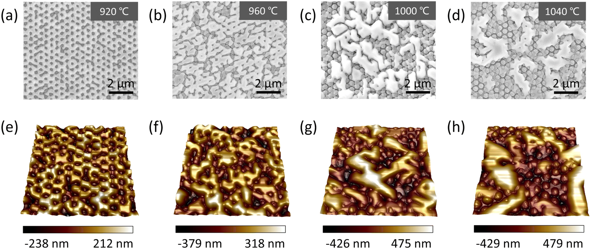 | ||
| Fig. 2 Plane-view SEM images of interrupted samples after 3D GaN growth on NPSS using LT-GaN NLs, corresponding to 3D temperatures of (a) 920 °C, (b) 960 °C, (c) 1000 °C, and (d) 1040 °C. All scale bars denote 2 μm. AFM images of these interrupted samples with 3D temperatures of (e) 920 °C, (f) 960 °C, (g) 1000 °C, and (h) 1040 °C. The AFM images correspond to 5 μm square regions. | ||
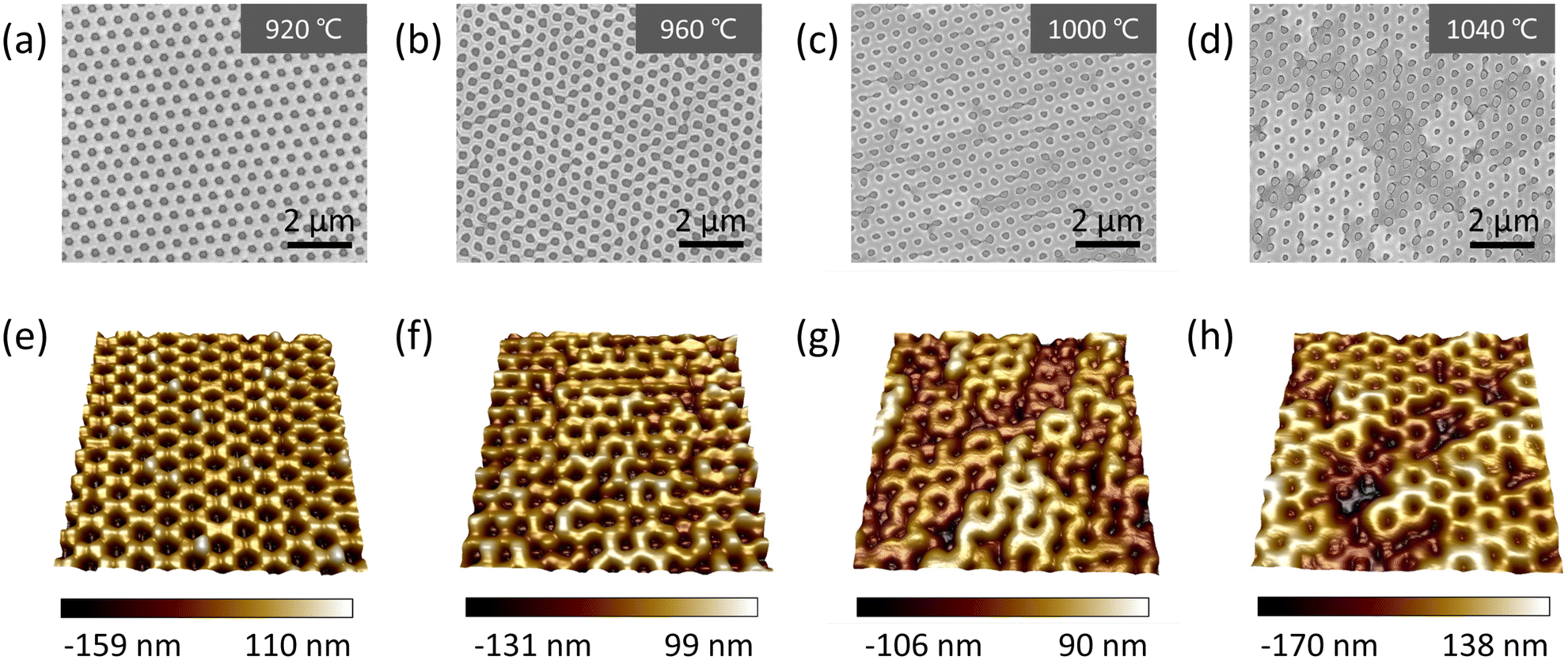 | ||
| Fig. 3 Plane-view SEM images of interrupted samples after 3D GaN growth on NPSS using PVD-AlN NLs, corresponding to 3D temperatures of (a) 920 °C, (b) 960 °C, (c) 1000 °C, and (d) 1040 °C. All scale bars denote 2 μm. AFM images of these interrupted samples with 3D temperatures of (e) 920 °C, (f) 960 °C, (g) 1000 °C, and (h) 1040 °C. The AFM images correspond to 5 μm square regions. | ||
Fig. 2 shows the surface morphology of 3D GaN grains grown on the NPSS with LT-GaN NLs. The SEM and AFM images show that as the 3D temperatures increase from 920 °C to 1040 °C, the distribution of 3D GaN grains becomes inhomogeneous, accompanied by grain density reduction and grain size increase. For quantitative statistics, the grains with incompletely coalesced crystal facets are considered as individual grains. From the SEM statistics, the average densities of the 3D GaN grains of samples A1–A4 are 4.5 × 108 cm−2, 3.9 × 108 cm−2, 2.3 × 108 cm−2, and 1.1 × 108 cm−2, respectively. Meanwhile, the average lateral sizes of their 3D GaN grains are 385 nm, 573 nm, 827 nm, and 1.21 μm, respectively. The cross-sectional SEM images indicate that the average heights of the 3D GaN grains are 424 nm, 542 nm, 663 nm, and 855 nm, respectively. The AFM statistics show that the standard height deviations of these samples are 63 nm, 95 nm, 120 nm, and 136 nm, respectively. These results indicate that severe Ostwald ripening of 3D GaN grains grown on NPSS was observed at high 3D temperatures, which quite differs from the situation observed on MPSS.35,36 Meanwhile, a relatively low 3D temperature is beneficial to the uniform distribution of 3D GaN grains on NPSS with LT-GaN NLs.
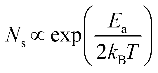
In fact, the saturation density of GaN grains can be obtained by solving the rate equation considering the adsorption, diffusion, and desorption of Ga atoms.37 At high temperatures, the saturation grain density is primarily controlled by Ga adatom desorption, while at low temperatures, it is mainly determined by surface diffusion.34 The saturation density Ns at different temperatures can be expressed as:34,37
High temperature:
 | (1) |
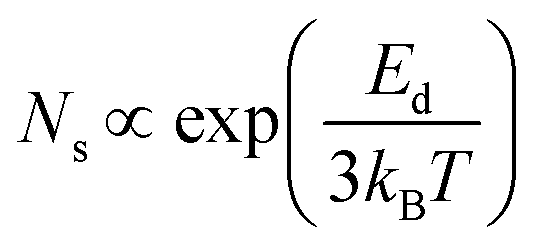 | (2) |
Fig. 3 displays the SEM and AFM images of 3D GaN grains grown on NPSS with PVD-AlN NLs. Impressively, GaN grains can achieve uniform growth on the NPSS with the PVD-AlN NLs even at 3D temperatures up to 1040 °C, which is quite different from the situation using LT-GaN NLs. As seen in Fig. 3(d) and (h), only slight Ostwald ripening of GaN grains occurs at the 3D temperature of 1040 °C. The cross-sectional SEM images indicate that the average heights of the 3D GaN grains are 563 nm, 498 nm, 381 nm, and 325 nm, respectively. The AFM statistics show that the standard height deviations of samples B1–B4 are 37 nm, 41 nm, 36 nm, and 47 nm, respectively. These results reveal that as the 3D temperature varies from 920 to 1040 °C, the growth of GaN grains on the NPSS with PVD-AlN NLs is gradually shifted towards 2D growth. Notably, the GaN grains maintain a highly homogeneous distribution despite the 3D temperature changes.
For the same 3D temperature conditions, the only difference between samples A1–A4 and samples B1–B4 is the type of NL. Compared with the LT-GaN NLs, the PVD-AlN NLs can substantially improve the growth uniformity of GaN grains on the NPSS. The LT-GaN NLs turn into small GaN grains after annealing at 3D temperatures, leading to inhomogeneous distribution of 3D GaN grains. In contrast, 3D GaN grains on PVD-AlN NLs are uniformly covered with the NPSS. Moreover, the surface diffusion and desorption barriers of Al adatoms on the sapphire (0001) surface are larger than those of Ga adatoms due to the higher AlN bond energy (2.88 eV) than GaN bond energy (2.24 eV).38 Thus, the PVD-AlN NLs exhibit better distribution homogeneity compared to the LT-GaN NLs, which promotes the uniform growth of 3D GaN grains on the NPSS.
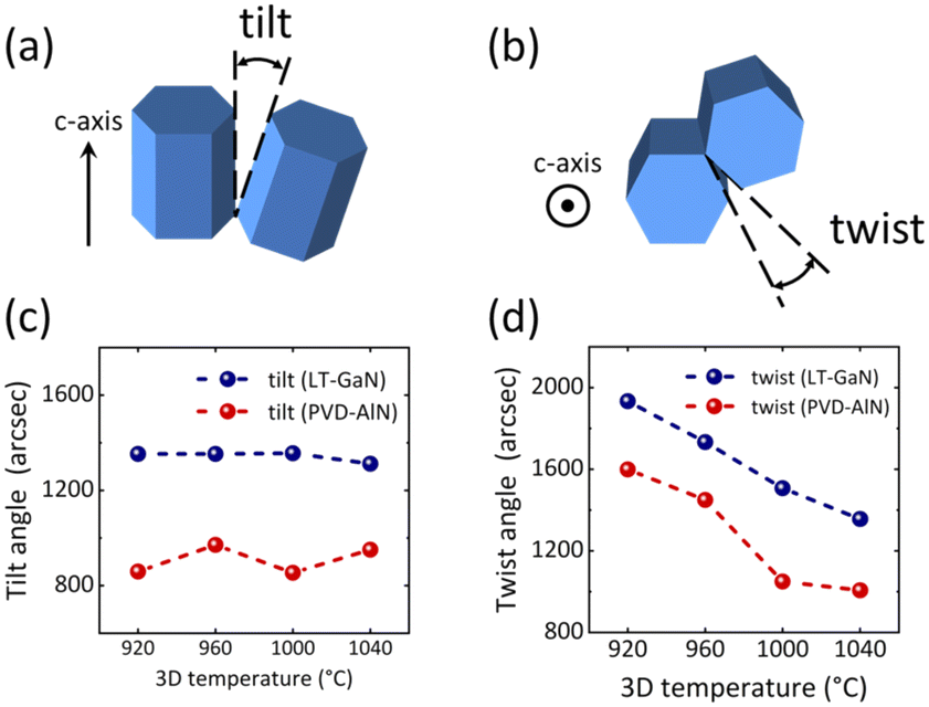
The grain coalescence process significantly affects dislocation formation and stress evolution in GaN films on the NPSS. The formation of screw and edge dislocations during grain coalescence is related to the tilting and twisting between GaN grain columns.27,28Fig. 4(a) and (b) illustrate the schematic diagram of the tilt angle and twist angle between GaN grain columns. In fact, the average tilt and twist angles of GaN grain columns can be determined by XRD from the ω-scans at different symmetrical reflections and the ω/φ-scans at asymmetrical reflections.39,40 The tilt angle βtilt between GaN grain columns can be acquired by ω-scans in the (000l) planes.41 The dependence between the measured full-width at half-maximum (FWHM) of the ω-scan ω(000l) and the tilt angle βtilt is shown below:41
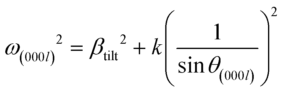 | (3) |
![[thin space (1/6-em)]](https://www.rsc.org/images/entities/char_2009.gif) θ(000l))2. Obviously, we can use the intersection to derive the tilt angles.
θ(000l))2. Obviously, we can use the intersection to derive the tilt angles.
 | ||
| Fig. 4 Schematic diagram of (a) tilt angle and (b) twist angle between GaN grain columns. (c) Tilt and (d) twist angles of the samples A1–A4 and B1–B4 after 3D growth calculated from the ω-scans for symmetrical planes and ω/φ-scans for asymmetrical planes. | ||
Theoretically, the twist angle βtwist between GaN grain columns can be acquired by ω/φ-scans perpendicular to the (000l) planes, with an inclination angle χ of 90°. In fact, as χ increases from 0° to 90°, the FWHMs of the ω-scan and φ-scan gradually converge. The twist angle can be accurately obtained by using ω-scans and φ-scans for planes corresponding to a χ approaching 90°, as the (121) plane corresponding to a χ of 78.6°.42 The twist angles can be taken as the average of the FWHM of the ω-scan and φ-scan from the (121) reflection:42
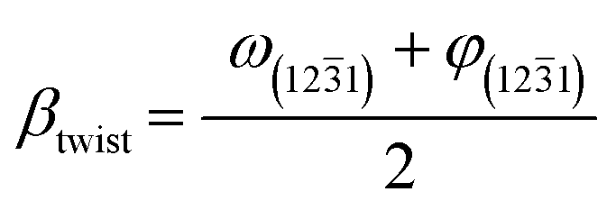 | (4) |
Fig. 4(c) and (d) show the measured tilt and twist angles of 3D GaN grain columns grown on NPSS with LT-GaN NLs and PVD-AlN NLs. As the 3D temperatures increase from 920 °C to 1040 °C, the tilt angles of GaN grains on NPSS have no significant change, while the twist angles gradually decrease. Actually, the spatial confinement effect of the periodic nanopatterns of NPSS is mainly in the dimension within the growth plane, whereas it hardly provides a confinement effect on the c-axis of the growth direction. In other words, the nanopatterns of the NPSS are mainly effective in limiting the twisting of GaN grains while hardly limiting the tilting of GaN grains. As a result, the tilt angle of the GaN grains remains almost unchanged at different 3D temperatures. As the 3D temperatures increase from 920 °C to 1040 °C, Ostwald ripening of GaN grains is observed, accompanied by a decrease in grain density and an increase in grain size, especially for the LT-GaN NLs. With smaller size and higher density, GaN grains are more prone to twist. When the size of the GaN grains increases, the GaN grains are less susceptible to twist due to their stronger connection to the substrate.
A comparison of LT-GaN and PVD-AlN NLs indicates that PVD-AlN NLs drastically reduce the tilt and twist angles of GaN grains on the NPSS. As shown in Fig. 4(c) and (d), the average tilt angle of GaN grains grown on PVD-AlN NLs is reduced from 1345 to 910 arcsec, and the twist angles are also reduced by about 25% on average compared to the LT-GaN NLs. In fact, the PVD-AlN NLs exhibit superior orientation uniformity and thermal stability.31,38,43 Moreover, the GaN grains have more stable connections with the PVD AlN NLs due to the higher surface diffusion and desorption barriers of Ga adatoms.44–46 Accordingly, the 3D GaN grains grown on NPSS with PVD-AlN NLs show smaller tilt and twist angles than those on LT-GaN NLs.
To explore the evolution of grain coalescence, the morphology of GaN grains before coalescence was analysed in detail. Fig. 5(a–d) show the cross-sectional and plane-view SEM images of 3D growth-interrupted samples A1 and B1 with a 3D temperature of 920 °C. In Fig. 5(a) and (c), GaN grains grown on LT-GaN NLs vary in lateral size and height, resulting in different areas and growth rates of the crystal facets before coalescence. Growth competition exists between these crystal facets, leading to the gradual annihilation of the small-area facets. The large-area crystal facets continue to grow due to faster growth rates. In contrast, GaN grown on PVD-AlN NLs is highly uniform in grain size, as shown in Fig. 5(b) and (d). It makes the GaN crystal facets converge toward the centre with similar growth rates.
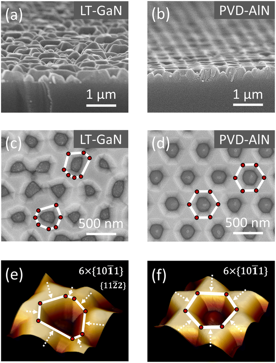 | ||
| Fig. 5 Cross-sectional SEM images of the interrupted samples of A1 and B1 after 3D growth on NPSS with (a) LT-GaN and (b) PVD-AlN NLs. Plane-view SEM images of these interrupted samples with (c) LT-GaN and (d) PVD-AlN NLs. 3D AFM images of these interrupted samples with (e) LT-GaN and (f) PVD-AlN NLs. The white boxes and red dots depict the GaN sidewall profile, and the white dashed lines with arrows indicate the GaN growth rates along growth directions. | ||
The orientation of GaN crystal planes affects the dislocation formation and stress evolution during coalescence. The crystal facets of 3D GaN grains can be determined by measuring sidewall inclination angles from cross-sectional SEM and AFM images. For 3D GaN grains grown on LT-GaN NLs, the inclined facets in the top region of nanopatterns were composed of 6 × {10![[1 with combining macron]](https://www.rsc.org/images/entities/char_0031_0304.gif) 1} and a few {11
1} and a few {11![[2 with combining macron]](https://www.rsc.org/images/entities/char_0032_0304.gif) 2}, as shown in Fig. 5(c) and (e). The growth competition between {101} and {112} crystal facets corresponds to concave growth, where a faster growth rate represents an expanded area.47,48 Under high-pressure, low-V/III-ratio conditions, the growth rates of {112} planes decrease more rapidly with lower temperature compared to the {101} planes.49,50 Thus, the predominance of {101} facets is mainly due to the faster growth rate of the {101} facets than the {112} facets at a 3D temperature of 920 °C.47,48 During the lateral growth process, some of the small-area {101} crystal facets tend to annihilate, while the large-area facets are retained. Eventually, coalescence occurs between these retained neighboring crystal facets, likely generating dislocations and introducing tensile stress.31 For 3D GaN grains grown on PVD-AlN NLs, the inclined facets are all composed of 6 × {101}, as shown in Fig. 5(d) and (f). These facets are highly consistent in size and orientation. During lateral growth, the coalescence areas of these facets will shrink into a point-like region. Meanwhile, these GaN grains exhibit less tilting and twisting than those on LT-GaN NLs, as shown in Fig. 4. Therefore, it is expected that the small-area coalescence between these small-angle tilted and twisted GaN grains on PVD-AlN NLs will introduce fewer dislocations and less tensile stress.
2}, as shown in Fig. 5(c) and (e). The growth competition between {101} and {112} crystal facets corresponds to concave growth, where a faster growth rate represents an expanded area.47,48 Under high-pressure, low-V/III-ratio conditions, the growth rates of {112} planes decrease more rapidly with lower temperature compared to the {101} planes.49,50 Thus, the predominance of {101} facets is mainly due to the faster growth rate of the {101} facets than the {112} facets at a 3D temperature of 920 °C.47,48 During the lateral growth process, some of the small-area {101} crystal facets tend to annihilate, while the large-area facets are retained. Eventually, coalescence occurs between these retained neighboring crystal facets, likely generating dislocations and introducing tensile stress.31 For 3D GaN grains grown on PVD-AlN NLs, the inclined facets are all composed of 6 × {101}, as shown in Fig. 5(d) and (f). These facets are highly consistent in size and orientation. During lateral growth, the coalescence areas of these facets will shrink into a point-like region. Meanwhile, these GaN grains exhibit less tilting and twisting than those on LT-GaN NLs, as shown in Fig. 4. Therefore, it is expected that the small-area coalescence between these small-angle tilted and twisted GaN grains on PVD-AlN NLs will introduce fewer dislocations and less tensile stress.
Dislocation and stress in GaN films after coalescence
Fig. 6 presents the in situ reflectance transients during the growth of GaN films for samples A4 and B4. From the SEM and AFM images in Fig. 2, GaN grains grown on the LT-GaN NLs suffer from severe Ostwald ripening. In this case, the GaN grains undergo an extended lateral growth process before coalescence occurs, which leads to a substantial increase in the coalescence thickness. The reflectance curve corresponding to the GaN films grown on the LT-GaN NLs starts to oscillate after about 2000 s. In contrast, the oscillation started from 500 s when using PVD-AlN NLs. As seen in Fig. 3, using PVD-AlN NLs significantly improves the growth uniformity of 3D GaN grains, resulting in smaller GaN grain size and higher grain density. It is reported that the coalescence thickness of GaN grown on NPSS is as low as 250 nm owing to the rapid coalescence of small-sized high-density GaN grains after a short transverse growth process.32 Moreover, the GaN islands on AlN NLs show less tilting and twisting to each other, similar to the orientation symmetry of patterned AlN.31 Therefore, the PVD-AlN NLs drastically reduce the coalescence thickness of GaN grains grown on the NPSS compared to the LT-GaN NLs.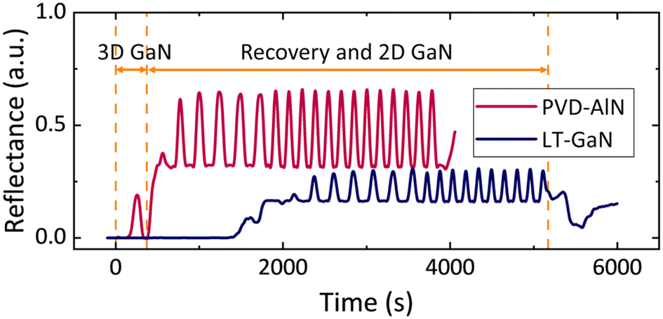 | ||
| Fig. 6 In situ reflectance (at 633 nm) transients vs. time during the growth of GaN films for samples A4 and B4. | ||
To investigate the effect of grain coalescence on dislocation formation in GaN films, XRD measurements were performed on samples A1–A4 and B1–B4. The FWHMs of ω-scans in the (0002) and (102) planes are shown in Fig. 7(a) and listed in Table 1. The results show that as the 3D temperatures increase, the screw dislocation densities in GaN films remain essentially unchanged, while the edge dislocation densities decrease significantly. Combined with the surface morphology of 3D GaN grains before coalescence shown in Fig. 2 and 3, higher 3D temperatures lead to lower grain densities and larger grain sizes. Previous studies have shown that the coalescence of low-density and large-size GaN grains introduces less edge dislocation density due to fewer coalescence boundaries.25,51 However, screw dislocations in GaN films on NPSS are related to grain tilting, which is independent of the coalescence process. Combined with the XRD results in Fig. 4(b) and (c), higher 3D temperatures contribute to reducing the twisting of GaN grains but have no obvious restriction on tilting. These observations imply that higher 3D temperatures contribute to lower edge dislocation densities without affecting the screw dislocation density.
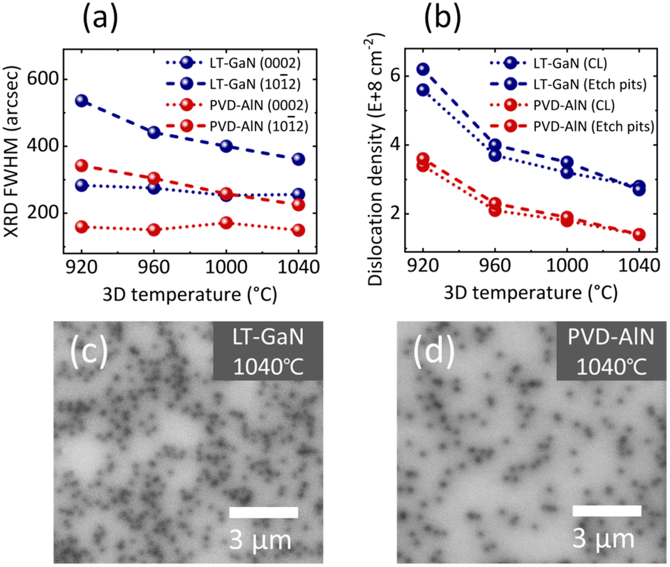 | ||
| Fig. 7 (a) XRD FWHMs of the (0002) and (102) planes of GaN films. (b) Variation of dislocation densities in GaN films grown on NPSS with different 3D temperatures obtained by CL imaging and counting etch pits by AFM. Plane-view CL mapping of GaN films for (c) sample A4 with LT-GaN NLs and (d) sample B4 with PVD-AlN NLs. | ||
2) planes, dislocation densities derived from CL and AFM results, and residual stresses obtained from E2(H) phonon frequency shifts of GaN films in the samples A1–A4 and B1–B4
| Sample | 3D temperature (°C) | XRD (0002) | XRD (102) |
Dislocation density (cm−2) | Raman shift (cm−1) | Residual stress (GPa) | ||
|---|---|---|---|---|---|---|---|---|
| CL imaging | Etch pits | |||||||
| NPSS/LT-GaN | A1 | 920 | 283 | 536 | 5.6 × 10⁸ | 6.2 × 10⁸ | 569.4 | 0.55 |
| A2 | 960 | 275 | 441 | 3.7 × 10⁸ | 4.0 × 10⁸ | 569.7 | 0.66 | |
| A3 | 1000 | 253 | 400 | 3.2 × 10⁸ | 3.5 × 10⁸ | 570.2 | 0.86 | |
| A4 | 1040 | 256 | 361 | 2.8 × 10⁸ | 2.7 × 10⁸ | 570.5 | 0.98 | |
| NPSS/PVD-AlN | B1 | 920 | 159 | 342 | 3.4 × 10⁸ | 3.6 × 10⁸ | 570.8 | 1.09 |
| B2 | 960 | 150 | 304 | 2.1 × 10⁸ | 2.3 × 10⁸ | 571.2 | 1.25 | |
| B3 | 1000 | 171 | 258 | 1.8 × 10⁸ | 1.9 × 10⁸ | 571.4 | 1.33 | |
| B4 | 1040 | 149 | 225 | 1.4 × 10⁸ | 1.4 × 10⁸ | 571.6 | 1.41 | |
In order to obtain dislocation densities, the methods of counting etch pits by AFM and counting dark spots in cathodoluminescence (CL) images were applied, as shown in Fig. 7(b) and Table 1. By comparing the dislocation densities of GaN films on LT-GaN and PVD-AlN NLs, it is evident that PVD-AlN NLs significantly improve the crystal quality of GaN films on NPSS. Combined with the XRD FWHM results, it can be seen that both the screw and edge dislocation densities of GaN films on PVD-AlN NLs decrease by over 40% compared to the LT-GaN NLs. Fig. 7(c) and (d) show the CL images of GaN films for samples A4 and B4. The dislocation densities are much smaller than the nanopattern densities, implying that not all the cone-shaped patterns have dislocations in the top regions. From the surface morphology of the 3D GaN grains in Fig. 3, the GaN grains grown on PVD-AlN NLs exhibit a high density of coalescence, mainly located in the top region of the cone-shaped pattern. Generally, a higher density of coalescence corresponds to a higher density of dislocations.25,29,51 Nevertheless, for GaN grains on PVD-AlN NLs, the high-density coalescence does not introduce excessive dislocations compared to LT-GaN NLs. Therefore, microscopic observation is required to investigate the dislocation distribution at the coalescence boundaries.
Dark-field TEM was employed to analyse the dislocation distribution at the GaN grain coalescence boundaries. Fig. 8 shows the dark-field TEM images of GaN films for samples A4 and B4. In Fig. 8(a), it can be clearly seen that the LT-GaN NLs transform into small GaN grains after annealing at 3D temperatures, where those on the cone-shaped pattern fail to grow further due to the lack of stable crystal facets. In contrast, the PVD-AlN NLs are uniformly covered on the NPSS after annealing, as shown in Fig. 8(c). The superior thermal stability of PVD-AlN NLs contributes to maintaining the uniform distribution of 3D GaN grains. Fig. 8(b) reveals that the dislocations in the GaN films grown on the NPSS with LT-GaN NLs primarily originate from the coalescence region at the top of the cone-shaped nanopatterns. In this experiment, the nanopattern density of the NPSS reaches approximately 4.5 × 108 cm−2. Therefore, grain coalescence at the top region of the cone-shaped nanopatterns introduces high-density dislocations in the GaN films grown on LT-GaN NLs. However, for GaN films grown on NPSSs with PVD-AlN NLs, much fewer dislocations are observed at the top region of the nanopatterns, as seen in Fig. 8(d). Combined with the XRD results in Fig. 4, the PVD-AlN NLs drastically reduce the tilt and twist angles of GaN grains compared to LT-GaN NLs. Moreover, the GaN grains on PVD-AlN NLs exhibit high consistency in size and orientation, leading to the coalescence areas shrinking to point-like regions, as discussed in Fig. 5. Accordingly, the coalescence process in small areas between small-angle tilted and twisted GaN grains grown on PVD-AlN NLs is likely to generate fewer dislocations.
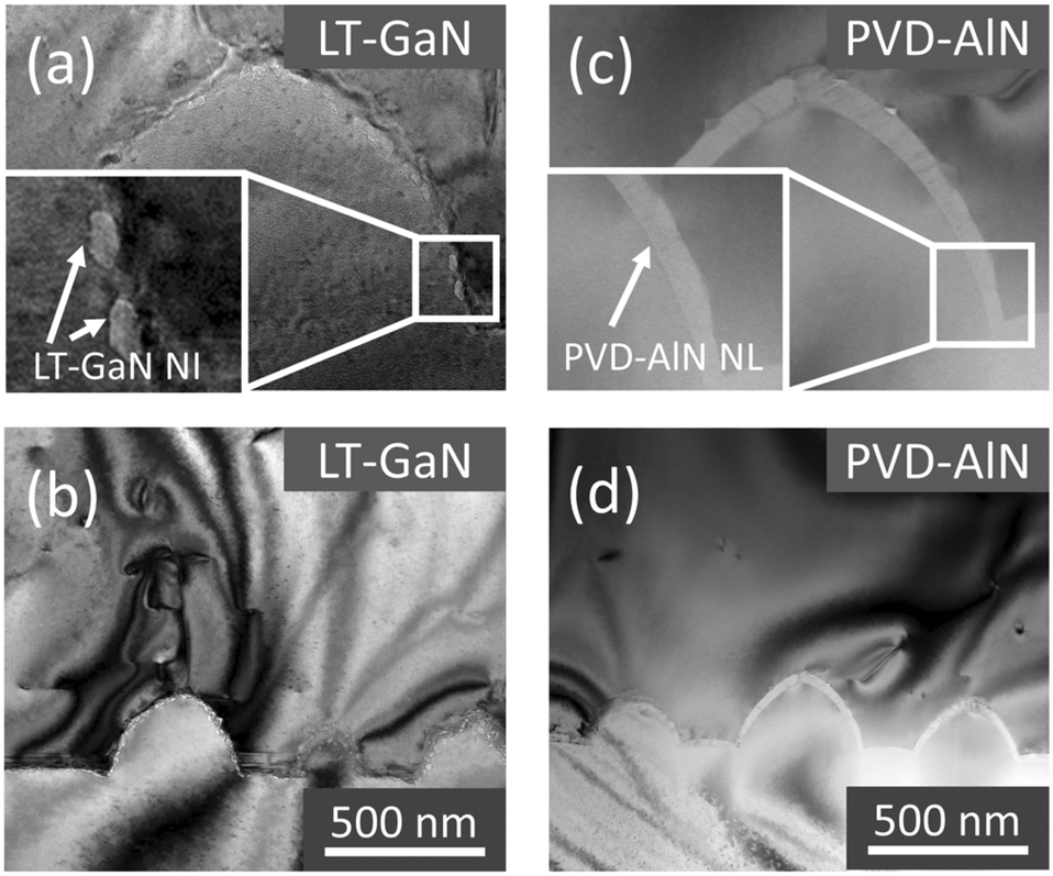 | ||
| Fig. 8 Cross-sectional TEM images of GaN films for (a and b) sample A4 with LT-GaN NLs and (c and d) sample B4 with PVD-AlN NLs. | ||
To explore the effect of grain coalescence on the stress in GaN films, Raman spectroscopy was applied to measure the residual stresses of samples A1–A4 and B1–B4. In fact, the observed residual stress in GaN films is the sum of the extrinsic compressive stress due to the thermal expansion mismatch to the sapphire and the intrinsic tensile stress which develops during grain coalescence.25Fig. 9(a) and (b) illustrate the Raman spectra of GaN films grown on NPSS with LT-GaN and PVD-AlN NLs at different 3D temperatures. The stress in GaN films can be calculated from the shift of the peak position of GaN E2(H) phonons. Specifically, the relationship between the in-plane stress σxx and E2(H) phonon frequency shift Δω in the GaN film can be expressed as:
| Δω = Kσxx | (5) |
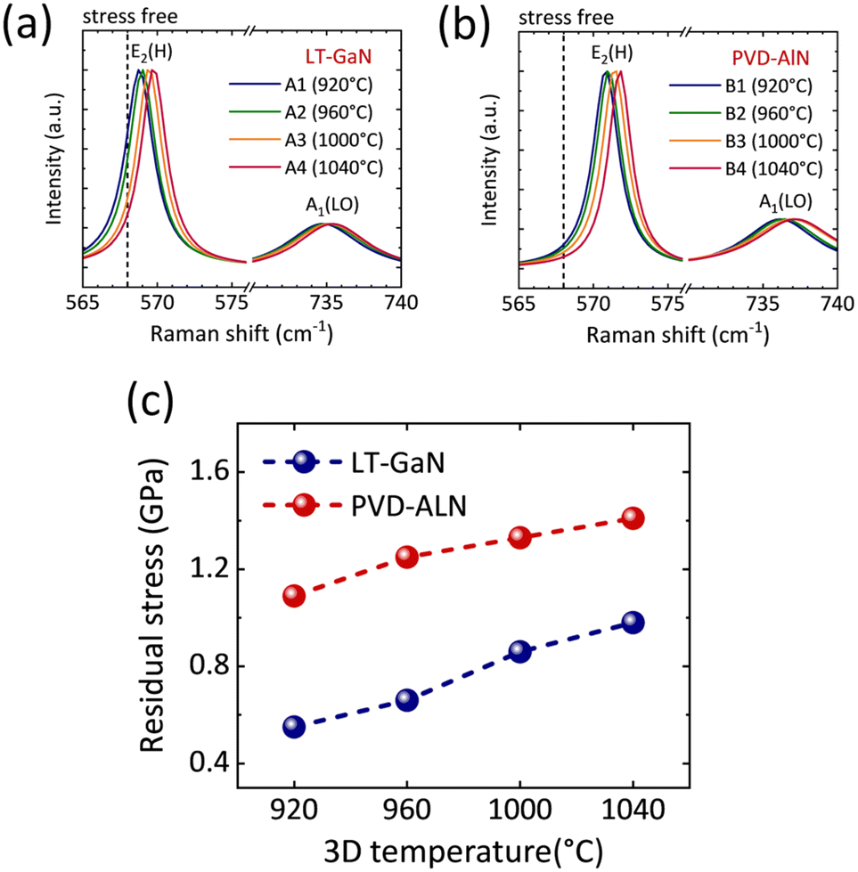 | ||
| Fig. 9 Raman spectra of GaN films grown on NPSS with (a) LT-GaN NLs and (b) PVD-AlN NLs at different 3D temperatures. (c) The residual compressive stresses calculated from the GaN E2(H) phonon peak position. | ||
Fig. 9(c) illustrates the residual compressive stresses of GaN films calculated from the E2(H) phonon frequency shift. As the 3D temperature increases from 920 to 1040 °C, the residual compressive stress of GaN on NPSS with LT-GaN NLs increases from 0.55 GPa to 0.98 GPa. It indicates that higher 3D temperatures lead to a reduction in the tensile stress introduced during coalescence. The tensile stress induced by GaN grain coalescence during growth is strongly correlated with the GaN grain size. The relationship between the tensile stress σ introduced by grain coalescence and the lateral grain size a can be expressed as follows:24,25
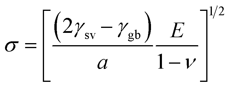 | (6) |
Confocal Raman mapping with a spatial resolution of 300 nm was employed to study the stress distribution of GaN films grown on NPSSs with PVD-AlN NLs. Fig. 10(a) and (b) show the peak intensity maps of GaN E2(H) phonon for sample B4 in the plane perpendicular and parallel to the c-axis. Fig. 10(c) and (d) display the corresponding stress distribution obtained from the GaN E2(H) phonon peak position fitted by the Voigt function. In Fig. 10(a), a clear NPSS periodic nanopattern can be observed in the peak intensity map of GaN E2(H) phonons in the c-plane, which is mainly attributed to the difference in light extraction efficiency. Fig. 10(c) displays the corresponding stress distribution, indicating discrete dark spots and continuous bright regions. The dark spots represent the locations of GaN grain coalescence. As a result of the coalescence process, the residual compressive stresses at these locations are reduced due to the introduction of tensile stresses. Obviously, the density of dark spots representing the coalescence locations is significantly lower than the density of the NPSS pattern, mainly attributed to the coalescence between large-size GaN grains resulting from Ostwald ripening, as shown in Fig. 3(d) and (h). Specifically, the GaN E2(H) peak positions at the dark spots and bright regions diverge by about 0.5 cm−1, as shown in Fig. 10(e). It indicates that the GaN at the dark spots locally introduces a tensile stress of about 0.2 GPa due to the grain coalescence process.
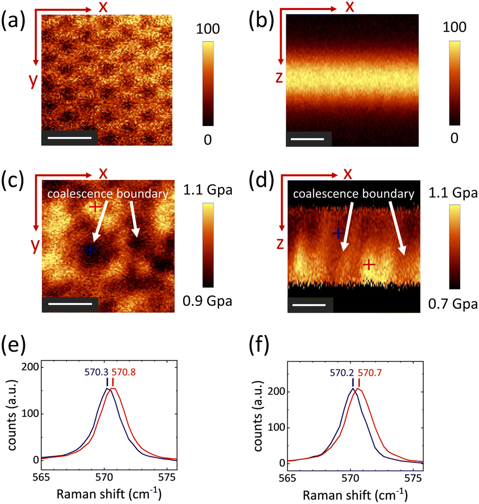 | ||
| Fig. 10 Raman mapping of GaN E2(H) phonon peak intensity in the plane (a) perpendicular and (b) parallel to the GaN c-axis direction of sample B4. The corresponding residual compressive stress distribution obtained from the GaN E2(H) phonon peak position fitted by the Voigt function in the plane (c) perpendicular and (d) parallel to the c-axis direction of sample B4. (e and f) Raman spectra of the points selected in (c and d). The x–y plane is perpendicular to the c-axis direction, and the z-axis is parallel to the c-axis direction. All scale bars denote 1 μm. | ||
From the Raman mapping in the plane parallel to the c-axis shown in Fig. 10(b) and (d), it can be seen that the stress distribution of the GaN near the substrate is relatively inhomogeneous. This stress inhomogeneity is mainly attributed to the tensile stress induced by grain coalescence during the early growth stages. After the completion of grain coalescence, the stress distribution in the 2D GaN layer becomes uniform. In Fig. 10(d), the dark areas near the substrate represent the locations where grain coalescence occurs, and the local residual compressive stresses are reduced due to the tensile stresses introduced by the coalescence process. Fig. 10(f) illustrates the Raman spectra of selected points in the dark and bright regions near the substrate. The GaN E2(H) peak positions at the dark and bright regions differ by about 0.5 cm−1, corresponding to about 0.2 GPa, similar to that observed in the plane perpendicular to the c-axis. These Raman mapping results for the stress distribution in GaN films on NPSS align with our prior findings obtained through CL mapping.13
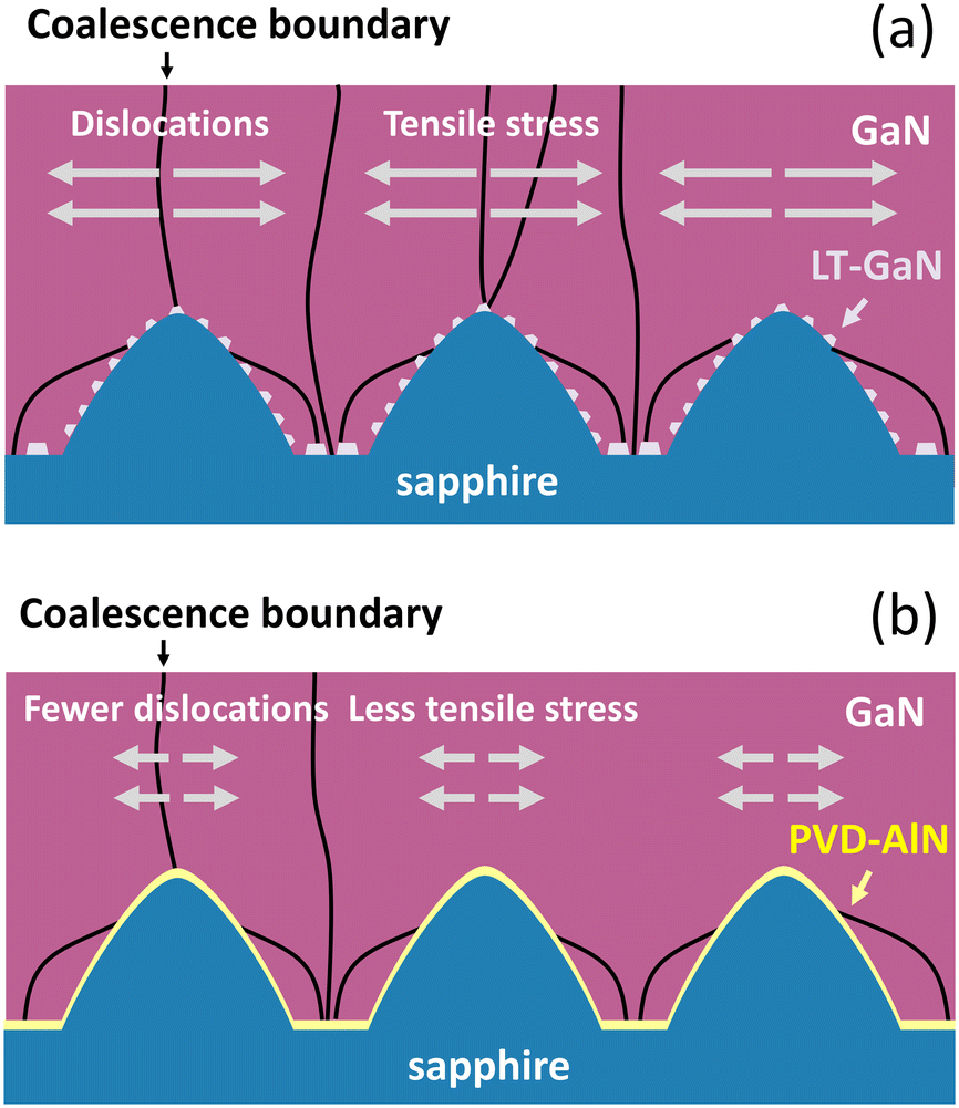
Fig. 11(a) and (b) show schematic diagrams illustrating the effect of grain coalescence on the dislocation and stress in GaN films grown on NPSS with LT-GaN NLs and PVD-AlN NLs. In the initial stages, the LT-GaN NLs transform into small GaN grains after annealing at 3D temperatures, while the PVD-AlN NLs remain uniformly coated on the NPSS due to their high Al–N bond energy. Concerning the LT-GaN NLs, the eventual coalescence of GaN grains on LT-GaN NLs occurs between large-area crystal facets due to the growth competition. Moreover, large-angle tilting and twisting exist between these GaN grains before coalescence. Therefore, the coalescence of GaN grains on LT-GaN NLs introduces more dislocations and greater tensile stress at the coalescence boundaries, as depicted in Fig. 11(a).
 | ||
| Fig. 11 Schematic diagram of dislocations and stress in GaN films grown on NPSS with (a) LT-GaN and (b) PVD-AlN NLs. | ||
In contrast, PVD-AlN NLs can effectively suppress the tilting and twisting of GaN grains and promote the orientation consistency of crystal facets during coalescence. The coalescence process in point-like regions between small-angle tilted and twisted GaN grains grown on PVD-AlN NLs generates few dislocations. A significant decrease in dislocation can be observed at the coalescence boundaries at the top of the cone-shaped pattern, as illustrated in Fig. 11(b). In addition, the coalescence of GaN grains grown on PVD-AlN introduces less tensile stress than that on LT-GaN NLs, mainly attributed to the point-like coalescence process.
In order to obtain high-quality GaN films on cone-shaped NPSSs, two significant challenges need to be addressed. One is the elimination of dislocations originating at the sapphire/GaN interface, and the other is the elimination of dislocations generated by grain coalescence. Dislocations at the interfaces are influenced by the proportion of the pattern area;53 thus the pattern periods and diameters need to be optimised. During lateral growth, the cone-shaped pattern of the NPSS can terminate part of the dislocations extending from the interface.12,13 However, the cone-shaped nanopattern with short height has a limited bending effect on dislocations compared to the MPSS.29,30 Therefore, a more rational NPSS pattern needs to be designed to bend the dislocations.
Moreover, grain coalescence without dislocation generation can be achieved when GaN grains are highly consistent in size and orientation.31 Actually, GaN grains at the trenches of neighbouring nanopatterns suffer from severe growth competition at high temperatures due to the weak Ga–N bond and small nanopattern period. Slight Ostwald ripening of GaN grains occurs despite introducing PVD-AlN to limit the diffusion and desorption of Ga atoms. It leads to difficulty in achieving grain coalescence with highly consistent size and orientation. Therefore, more effective methods for controlling GaN grain orientation are required to reduce dislocation density further.
Conclusions
In summary, the effect of grain coalescence on the dislocation and stress in GaN films grown on NPSSs with LT-GaN NLs and PVD-AlN NLs is comparably investigated. The results show that higher 3D temperatures can reduce the edge dislocation density induced by grain coalescence in GaN films on the NPSS. Meanwhile, higher 3D temperatures lead to a decrease in the tensile stress introduced by grain coalescence, consequently increasing the residual compressive stress in GaN films. Specifically for the LT-GaN NLs, higher 3D temperatures lead to severe Ostwald ripening, resulting in an inhomogeneous distribution of 3D GaN grains. The PVD-AlN NLs significantly enhance the uniformity of the GaN grain growth and reduce the coalescence thickness. Furthermore, the PVD-AlN NLs effectively minimize the tilt and twist angles of the 3D GaN grains and promote the orientation consistency of crystal facets, thereby reducing the density of screw and edge dislocations at the grain coalescence boundaries. In addition, the PVD-AlN NLs introduce additional residual compressive stress in the GaN films due to the intrinsic compressive stress from smaller AlN lattices and the reduced tensile stress arising from point-like coalescence.Conflicts of interest
There are no conflicts to declare.Acknowledgements
This work was supported by the National Key Research and Development Program of China (2021YFB3600100, 2022YFB3608501, 2023YFB4604401), the National Natural Science Foundation of China (62174004, 6192780, 81871427), the Basic and Applied Basic Research Foundation of Guangdong Province (2020B1515120020), and the Beijing-Tianjin-Hebei Special Project (J200014). The authors acknowledge the Electron Microscopy Laboratory of Peking University, China, for the use of ThermoFisher Helios G4 UX and FEI Tecnai F20 TEM.Notes and references
- J. J. Wierer and N. Tansu, Laser Photonics Rev., 2019, 13, 1900141 CrossRef.
- X. Zhou, P. Tian, C.-W. Sher, J. Wu, H. Liu, R. Liu and H.-C. Kuo, Prog. Quantum Electron., 2020, 71, 100263 CrossRef.
- W. C. Miao, F. H. Hsiao, Y. Sheng, T. Y. Lee, Y. H. Hong, C. W. Tsai, H. L. Chen, Z. Liu, C. L. Lin, R. J. Chung, Z. T. Ye, R. H. Horng, S. C. Chen, H. C. Kuo and J. H. He, Adv. Opt. Mater., 2023, 2300112 CrossRef.
- J. Xiong, E. L. Hsiang, Z. He, T. Zhan and S. T. Wu, Light: Sci. Appl., 2021, 10, 216 CrossRef CAS.
- X. Yang, Y. Lin, T. Wu, Z. Yan, Z. Chen, H.-C. Kuo and R. Zhang, Opto-Electron. Adv., 2022, 5, 210123 CAS.
- H. Gao, F. Yan, Y. Zhang, J. Li, Y. Zeng and G. Wang, J. Appl. Phys., 2008, 103, 014314 CrossRef.
- C.-H. Chan, C.-H. Hou, S.-Z. Tseng, T.-J. Chen, H.-T. Chien, F.-L. Hsiao, C.-C. Lee, Y.-L. Tsai and C.-C. Chen, Appl. Phys. Lett., 2009, 95, 011110 CrossRef.
- Y. Li, S. You, M. Zhu, L. Zhao, W. Hou, T. Detchprohm, Y. Taniguchi, N. Tamura, S. Tanaka and C. Wetzel, Appl. Phys. Lett., 2011, 98, 151102 CrossRef.
- S. Zhou, X. Zhao, P. Du, Z. Zhang, X. Liu, S. Liu and L. J. Guo, Nanoscale, 2022, 14, 4887–4907 RSC.
- A. Y. Polyakov and I.-H. Lee, Mater. Sci. Eng., R, 2015, 94, 1 CrossRef.
- A. David, N. G. Young, C. Lund and M. D. Craven, ECS J. Solid State Sci. Technol., 2019, 9, 016021 CrossRef.
- J. Z. Li, Z. Z. Chen, Q. Q. Jiao, Y. L. Feng, S. Jiang, Y. F. Chen, T. J. Yu, S. F. Li and G. Y. Zhang, CrystEngComm, 2015, 17, 4469 RSC.
- Y. Chen, Z. Chen, J. Li, Y. Chen, C. Li, J. Zhan, T. Yu, X. Kang, F. Jiao, S. Li, G. Zhang and B. Shen, CrystEngComm, 2018, 20, 6811 RSC.
- H. Wang, H. Sodabanlu, Y. Daigo, T. Seino, T. Nakagawa and M. Sugiyama, Appl. Phys. Express, 2016, 9, 055503 CrossRef.
- H. Wang, H. Sodabanlu, Y. Daigo, T. Seino, T. Nakagawa and M. Sugiyama, J. Cryst. Growth, 2017, 465, 12 CrossRef CAS.
- C. He, W. Zhao, K. Zhang, L. He, H. Wu, N. Liu, S. Zhang, X. Liu and Z. Chen, ACS Appl. Mater. Interfaces, 2017, 9, 43386 CrossRef CAS PubMed.
- N. Izyumskaya, V. Avrutin, K. Ding, Ü. Özgür, H. Morkoç and H. Fujioka, Semicond. Sci. Technol., 2019, 34, 093003 CrossRef CAS.
- R. Peng, Y. Hao, X. Meng, S. Xu, J. Zhang, P. Li, J. Huang, J. Du, Y. Zhao and X. Fan, IEEE Trans. Electron Devices, 2019, 66, 2243 CAS.
- S.-W. Chen, H. Li and T.-C. Lu, AIP Adv., 2016, 6, 045311 CrossRef.
- L.-C. Chang, Y.-A. Chen and C.-H. Kuo, IEEE Trans. Electron Devices, 2014, 61, 2443 CAS.
- H. Wang, Y. Daigo, T. Seino, S. Ishibashi and M. Sugiyama, Jpn. J. Appl. Phys., 2016, 55, 105501 CrossRef.
- H. Hu, S. Zhou, X. Liu, Y. Gao, C. Gui and S. Liu, Sci. Rep., 2017, 7, 44627 CrossRef.
- H. Hu, S. Zhou, H. Wan, X. Liu, N. Li and H. Xu, Sci. Rep., 2019, 9, 3447 CrossRef PubMed.
- W. D. Nix and B. M. Clemens, J. Mater. Res., 1999, 14, 3467 CrossRef CAS.
- T. Böttcher, S. Einfeldt, S. Figge, R. Chierchia, H. Heinke, D. Hommel and J. S. Speck, Appl. Phys. Lett., 2001, 78, 1976 CrossRef.
- X. H. Wu, P. Fini, E. J. Tarsa, B. Heying, S. Keller, U. K. Mishra, S. P. DenBaars and J. S. Speck, J. Cryst. Growth, 1998, 189, 231 CrossRef.
- H. Heinke, V. Kirchner, S. Einfeldt and D. Hommel, Appl. Phys. Lett., 2000, 77, 2145 CrossRef CAS.
- M. E. Vickers, M. J. Kappers, R. Datta, C. McAleese, T. M. Smeeton, F. D. G. Rayment and C. J. Humphreys, J. Phys. D: Appl. Phys., 2005, 38, A99 CrossRef CAS.
- W. Li, S. Xu, Y. Zhang, R. Peng, Y. Zhao, J. Du, X. Fan, J. Zhang, H. Tao, X. Wang and Y. Hao, Superlattices Microstruct., 2019, 134, 106221 CrossRef CAS.
- S. Zhou, H. Hu, X. Liu, M. Liu, X. Ding, C. Gui, S. Liu and L. J. Guo, Jpn. J. Appl. Phys., 2017, 56, 111001 CrossRef.
- J. Wang, N. Xie, F. Xu, L. Zhang, J. Lang, X. Kang, Z. Qin, X. Yang, N. Tang, X. Wang, W. Ge and B. Shen, Nat. Mater., 2023, 22, 853 CrossRef CAS PubMed.
- Y.-K. Ee, X.-H. Li, J. Biser, W. Cao, H. M. Chan, R. P. Vinci and N. Tansu, J. Cryst. Growth, 2010, 312, 1311 CrossRef CAS.
- D. D. Koleske, A. E. Wickenden, R. L. Henry, W. J. DeSisto and R. J. Gorman, J. Appl. Phys., 1998, 84, 1998 CrossRef CAS.
- F. Dwikusuma, J. Mayer and T. F. Kuech, J. Cryst. Growth, 2003, 258, 65 CrossRef CAS.
- S. Zhou, Z. Lin, H. Wang, T. Qiao, L. Zhong, Y. Lin, W. Wang, W. Yang and G. Li, J. Alloys Compd., 2014, 610, 498 CrossRef CAS.
- M.-T. Wang, F. Brunner, K.-Y. Liao, Y.-L. Li, S. H. Tseng and M. Weyers, J. Cryst. Growth, 2013, 363, 109 CrossRef CAS.
- V. N. E. Robinson and J. L. Robins, Thin Solid Films, 1974, 20, 155 CrossRef.
- H. Morkoç, Handbook of Nitride Semiconductors and Devices, 2009 Search PubMed.
- K. Kobayashi, A. A. Yamaguchi, S. Kimura, H. Sunakawa, A. Kimura and A. Usui, Jpn. J. Appl. Phys., 1999, 38, L611 CrossRef CAS.
- M. A. Moram and M. E. Vickers, Rep. Prog. Phys., 2009, 72, 036502 CrossRef.
- V. S. Harutyunyan, E. Zielińska-Rohozińska and M. Regulska, J. Alloys Compd., 2004, 362, 287 CrossRef CAS.
- X. H. Zheng, H. Chen, Z. B. Yan, Y. J. Han, H. B. Yu, D. S. Li, Q. Huang and J. M. Zhou, J. Cryst. Growth, 2003, 255, 63 CrossRef CAS.
- D. Liu, L. Hu, X. Yang, Z. Zhang, H. Yu, F. Zheng, Y. Feng, J. Wei, Z. Cai, Z. Chen, C. Ma, F. Xu, X. Wang, W. Ge, K. Liu, B. Huang and B. Shen, Adv. Funct. Mater., 2022, 32, 2113211 CrossRef CAS.
- R. M. Feenstra, Y. Dong, C. D. Lee and J. E. Northrup, J. Vac. Sci. Technol., B, 2005, 23, 1174 CrossRef CAS.
- T. Narita, Y. Honda, M. Yamaguchi and N. Sawaki, Phys. Status Solidi B, 2006, 243, 1665 CrossRef CAS.
- V. Jindal and F. Shahedipour-Sandvik, J. Appl. Phys., 2009, 105, 084902 CrossRef.
- Q. Sun, C. D. Yerino, B. Leung, J. Han and M. E. Coltrin, J. Appl. Phys., 2011, 110, 053517 CrossRef.
- B. Leung, Q. Sun, C. D. Yerino, J. Han and M. E. Coltrin, Semicond. Sci. Technol., 2012, 27, 024005 CrossRef.
- K. Hiramatsu, K. Nishiyama, A. Motogaito, H. Miyake, Y. Iyechika and T. Maeda, Phys. Status Solidi A, 1999, 176, 535 CrossRef CAS.
- K. Hiramatsu, K. Nishiyama, M. Onishi, H. Mizutani, M. Narukawa, A. Motogaito, H. Miyake, Y. Iyechika and T. Maeda, J. Cryst. Growth, 2000, 221, 316 CrossRef CAS.
- F. J. Xu, L. S. Zhang, N. Xie, M. X. Wang, Y. H. Sun, B. Y. Liu, W. K. Ge, X. Q. Wang and B. Shen, CrystEngComm, 2019, 21, 2490 RSC.
- H. Harima, J. Phys.: Condens. Matter, 2002, 14, R967 CrossRef CAS.
- L. Zhang, F. Xu, J. Wang, C. He, W. Guo, M. Wang, B. Sheng, L. Lu, Z. Qin, X. Wang and B. Shen, Sci. Rep., 2016, 6, 35934 CrossRef CAS PubMed.
| This journal is © The Royal Society of Chemistry 2024 |