
Ultralow thermal conductivity and high thermoelectric performance induced by multiscale lattice defects in Cu-doped BST alloys†
Yaohui
Liu
,
Yu
Tang
,
Yonggui
Tao
,
Ying
Zhang
,
Lanxian
Shen
,
Wen
Ge
 and
Shukang
Deng
*
and
Shukang
Deng
*
Education Ministry Key Laboratory of Renewable Energy Advanced Materials and Manufacturing Technology, Yunnan Normal University, Kunming 650500, China. E-mail: skdeng@126.com
First published on 1st December 2023
Abstract
This study focuses on the effect of Cu doping on the thermoelectric properties of BiSbTe3 (BST) alloys. Firstly, we successfully prepared high-quality BST alloys using the KCl solvent method and selected the most promising BST(KCl)3.5 sample from them, followed by Cu doping experiments. The experimental results show that Cu doping significantly improves the crystal quality and density of the alloy, thereby increasing the material's mobility and reducing the resistivity, leading to an improvement in the power factor. However, Cu doping also introduces a large number of dislocations and lattice distortions. Additionally, the highly doped samples contain Cu2Te and BST superlattice structures, which further enhance the scattering of heat transfer phonons, significantly reducing the lattice thermal conductivity. In the experiment, Cu-doped samples exhibited extremely low lattice thermal conductivity, as low as 0.32 W m−1 K−1 at 300 K. These improvements in structure and performance have greatly enhanced the thermoelectric efficiency of Cu-doped samples, leading to a significant increase in their ZT values. Particularly, in samples with a Cu doping level of x = 0.01, the maximum ZT value was 1.47 at 400 K, and the average ZT value reached 1.28 in the temperature range of 300 K to 450 K. These findings underscore the wide-ranging application potential of Cu-doped BiSbTe3 alloys in room temperature refrigeration and power generation. The study provides crucial insights into the characteristics of Cu-doped BiSbTe3 alloys, while also contributing to the optimization of thermoelectric material design and the advancement of sustainable energy conversion technologies.
1. Introduction
Faced with urgent challenges such as global energy shortages and the increasingly severe greenhouse effect, humanity faces enormous pressure to develop sustainable energy sources and protect the fragile environment of the Earth.1–5 The use of traditional energy sources has resulted in a significant waste of thermal energy, generated as by-products during the extraction and utilization of energy sources like coal, oil, and natural gas.6–11 This not only depletes valuable resources but also contributes to environmental issues. Simultaneously, the use of conventional refrigeration materials has adverse effects on the ozone layer, further exacerbating environmental degradation.12–17 Therefore, it is imperative to explore new refrigeration technologies that are both environmentally friendly and energy-efficient. In this context, thermoelectric materials have emerged as a revolutionary solution.18–27Thermoelectric materials possess the excellent ability to convert thermal energy into electrical energy.28–33 This enables them to harness and reuse energy from various sources, such as automotive exhaust, industrial waste heat, and geothermal resources.34–40 The conversion potential of these materials opens new possibilities for achieving sustainable energy development. Besides their energy conversion advantages, thermoelectric materials also offer other unique benefits. Their ability to achieve fast, precise, and noise-free cooling methods makes them highly favorable in various cooling applications.41–44 Additionally, the environmental characteristics of these materials align with the necessity of sustainable technological progress. The development and application of thermoelectric materials are expected to play a pivotal role in addressing the current energy crisis and environmental challenges.
BST (Bi–Sb–Te) based compounds and their alloys have extensive applications across multiple fields owing to their remarkable thermoelectric properties. Over the past few decades, extensive research has been conducted to continually enhance their thermoelectric performance, leading to the exploration of various methods. Among these, doping stands out as the most commonly employed approach to optimize their thermoelectric properties. Research has unequivocally demonstrated the favorable impact of Cu doping on the characteristics of BST alloys. For instance, consider the work of Jiang et al., who used thermal deformation and Cu doping to synergistically enhance Bi0.48Sb1.52Te3, ultimately achieving an impressive maximum ZT value of 1.1 at 400 K.45 Another notable study, carried out by Wu et al., utilized the Bridgman method to fabricate Cu-doped Bi–Te alloys, resulting in a peak ZT value of 1.2 at 300 K.46 Additionally, research by Lim et al. suggests that Cu doping can not only improve the thermoelectric performance but also enhance the controllability of (BiSb)2Te3 compounds by concurrently regulating charge and heat transfer. The introduction of Cu effectively mitigates the bipolar thermal diffusion effect and reduces the lattice thermal conductivity of the material, thereby enhancing the thermoelectric performance of the compound at relatively high temperatures and achieving a maximum ZT value of 1.1 within the detection temperature range.47 The aforementioned studies collectively suggest that Cu doping exhibits significant potential for fine-tuning the electrical transport performance and thermoelectric properties of BST-based alloys, laying a robust groundwork for further ZT value improvement. Although these advancements have significantly propelled the thermoelectric properties of BST alloys, the journey towards their widespread application remains arduous. Consequently, our plan is to employ a specialized Cu doping technique to further refine the thermoelectric performance and expedite the incorporation of BST alloys into practical applications.
In this work, the use of KCl as a solvent to prepare Cu-doped BST alloys represents a novel and significant method. The unique aspect of this preparation method lies in the dissolution of various elements in the KCl solvent under high-temperature conditions. During the BST alloy formation process, elements such as Bi, Sb, Te, and Cu can gradually be released from the KCl solvent. This process contributes to maintaining a balanced element content within the synthesized material, preventing excessive element loss and resulting in a more uniform element distribution. This uniformity is of paramount importance for enhancing material performance and stability. Furthermore, this preparation method is anticipated to enhance the crystal quality of the material and stabilize its internal structure, consequently improving the electrical transport performance of the material. In summary, the KCl solvent method for synthesizing BST alloys offers a promising approach for producing high-performance materials with uniformly distributed elements, and it is expected to exhibit outstanding performance in various practical applications.
2. Experimental section
The BiSbTe3 sample was prepared by the KCl solvent method combined with melting slow cooling technology. The samples were designated as BST(KCl)3.5, BST(KCl)5, BST(KCl)6.5, BST(KCl)8, and BST(KCl)9.5, corresponding to different stoichiometric ratios of BiSbTe3(KCl)x (x = 3.5, 5, 6.5, 8, and 9.5), respectively. Among these samples, BST(KCl)3.5 was selected as the base sample for further experiments. Cu doping experiments were performed on the BST(KCl)3.5 sample using various doping concentrations denoted as CuxBi1−xSbTe3·KCl3.5 (x = 0.01, 0.015, 0.02, 0.025, and 0.03), and labeled as S1, S2, S3, S4, and S5, respectively. Comprehensive investigations of the thermoelectric properties were conducted on all the samples. More detailed information regarding the material preparation and performance testing can be found in the ESI.†3. Results and discussion
Fig. 1(a) displays the XRD spectra of pure-BST samples and BST(KCl)x samples synthesized using KCl as a solvent. The main diffraction peaks of all samples correspond to the standard diffraction peak of the BiSbTe3 phase (PDF#72-1835), indicating that these synthesized BST alloys have a rhombohedron crystal structure and belong to the space group R![[3 with combining macron]](https://www.rsc.org/images/entities/char_0033_0304.gif) m. On the right, there is a locally enlarged image of the (110) crystal plane diffraction peak. In the BST(KCl)x sample, as x increases, the overall spectrum shifts towards higher angles, indicating a decrease in lattice parameters. The Bragg diffraction peak of the BST(KCl)x sample shifts towards a smaller angle compared to the pure-BST sample, indicating an increase in lattice parameters.
m. On the right, there is a locally enlarged image of the (110) crystal plane diffraction peak. In the BST(KCl)x sample, as x increases, the overall spectrum shifts towards higher angles, indicating a decrease in lattice parameters. The Bragg diffraction peak of the BST(KCl)x sample shifts towards a smaller angle compared to the pure-BST sample, indicating an increase in lattice parameters.
 | ||
| Fig. 1 (a) XRD pattern for BST samples and local amplifying patterns of the (110) diffraction peaks; (b) the atomic ratio obtained by EPMA for BST(KCl)x=0, 3.5, 5, 6.5, 8, 9.5 samples; (c) XRD detection results of KCl solvent; (d and e) SEM micrographs of the fracture surface of pure-BST and BST(KCl)3.5 samples. | ||
To investigate the potential correlation between changes in lattice parameters and specific element deletions in the prepared materials, electron probe microanalysis (EPMA) tests were conducted on all samples, and the results are shown in Fig. 1(b). The analysis of the results in the figure indicates that the content of the Te element in the pure BiSbTe3 sample is relatively low, suggesting the presence of a large number of Te vacancies in the material. These vacancies may be a result of the evaporation of Te elements during the preparation process and are also the reason for the missing diffraction peaks on the (101) and (021) crystal planes in the intrinsic samples. When KCl is used as a solvent, the constituent elements of the BST alloy dissolve in the KCl flux at high temperatures, which helps reduce their evaporation rate. As the BST alloy forms, the constituent elements are gradually released from the KCl solvent, thereby minimizing excessive loss of certain elements. Consequently, using KCl as a solvent helps maintain the relative equilibrium composition of the elements in the sample. Furthermore, according to the results of EPMA, as the amount of KCl solvent increases, the content of Bi and Sb elements in the synthesized samples gradually decreases. This phenomenon is mainly due to the increase in residual Sb and Bi content in the solvent as the x value increases in the BST(KCl)x sample, as shown in Fig. 1(c). As a result, this leads to a decrease in the content of Sb and Bi elements in the sample, resulting in a reduction in lattice parameters.
To study the microstructure difference between the intrinsic sample and the BST alloy sample prepared with KCl as the solvent, the cross sections of pure-BST and BST(KCl)3.5 samples were tested using a Scanning Electron Microscope (SEM). The results are shown in Fig. 1(d) and (e). Fig. 1(d) displays the cross-section of the pure BST sample. From the figure, it is evident that the cross-section of the intrinsic sample exhibits numerous macroscopic voids and defects. The material's layered structure appears as fine flakes, with fewer large layered structures, and the density between layers is poor. This structural configuration will severely impacts the mobility of charge carriers, consequently adversely affecting the material's electrical transport performance. In contrast, Fig. 1(e) shows the cross-sectional image of the BST(KCl)3.5 sample prepared using KCl as a solvent. The sample reveals a distinct large layered structure, with closely connected layers. While there are still interlayer gaps in certain areas within the sample, overall, the presence of macroscopic voids and defects is significantly reduced.
Based on the above analysis, compared to pure BST samples, BST(KCl)3.5 alloy samples prepared using KCl solvent exhibit a superior structure. This structural change has a positive impact on improving the transport rate of charge carriers between layers and is expected to make significant breakthroughs in reducing the material's resistivity. Therefore, further research can explore the possibility of using more solvent treatment methods to enhance the structure and properties of materials.
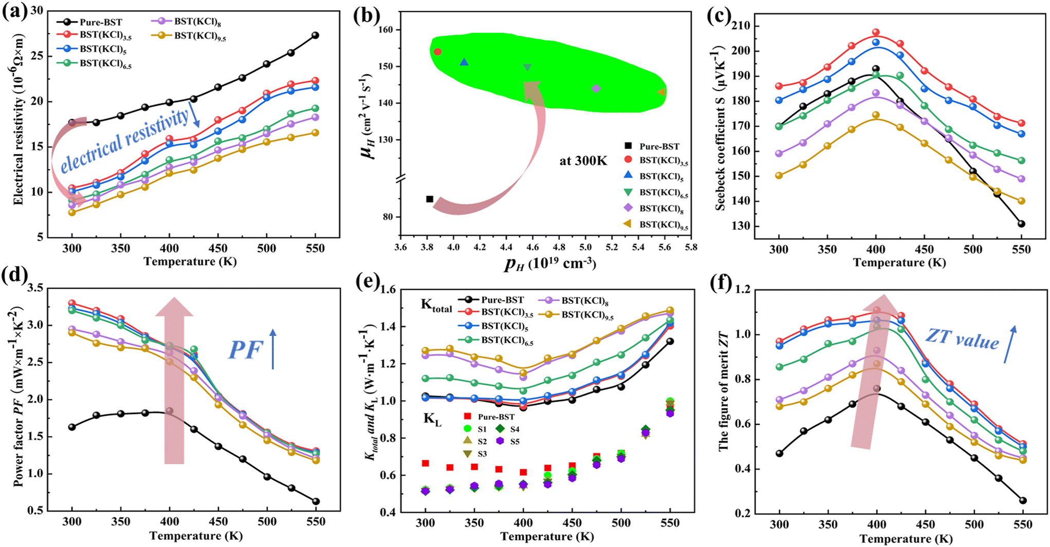
According to the relationship between the resistivity of the BST(KCl)x sample and temperature shown in Fig. 2(a), we observe that the resistivity of all samples gradually increases with temperature within the tested temperature range, which is in line with the typical characteristics of a degenerate semiconductor. However, in comparison to the pure-BST sample, the resistivity of all BST(KCl)x samples is effectively reduced. Specifically, at room temperature, the resistivity decreases from 17.6 (10−6 Ω m) to 7.8 (10−6 Ω m). The reduced resistivity can be attributed to two main reasons: firstly, as mentioned earlier, the significant reduction in the number of macroscopic voids in the BST(KCl)x sample leads to an increase in the material's density and an improvement in its crystal structure. This enhancement results in an increase in the carrier mobility of the material (see Fig. 2(c)). Secondly, the Hall test results indicate that the sample is a p-type semiconductor, and hole carriers play a dominant role in the transportation process. In the pure-BST sample, the absence of Te elements leads to the formation of VTe defects, resulting in the generation of additional electrons and a decrease in its own hole carrier concentration. The BST(KCl)x sample effectively suppresses the VTe defects, reducing the generation of additional electrons and increasing the concentration of its own hole carriers. Furthermore, the analysis showed that with the increase of KCl solvent content, the content of Bi and Sb elements dissolved in the solvent gradually increases, resulting in more Bi and Sb vacancies within the synthesized BST alloy sample. These defects can adsorb and neutralize some additional electrons, further increasing the concentration of hole carriers and reducing the material's resistivity.
 | ||
| Fig. 2 (a) Electrical resistivity for BST samples; (b) carrier concentration n and mobility μH; (d) PF; (c) the S values for BST samples; (e) κtotal and κL; (f) the figures of merit ZT. | ||
Fig. 2(c) illustrates the changes in the Seebeck coefficients of pure-BST and BST(KCl)x samples at different temperatures. The positive Seebeck coefficients in all samples indicate that the prepared BST alloy prepared is a p-type semiconductor, with hole as the main carrier type, consistent with the Hall test results (see ESI†). Within the temperature range of 300 K to 400 K, the Seebeck coefficients of all samples exhibit a rapid increase with the increase of temperature. This behavior suggests a significant bipolar diffusion phenomenon in BST alloys. Fig. 2(d) presents the power factor (PF) values of BST samples as a function of temperature. All BST(KCl)x samples demonstrate higher PF values than pure BST samples, with BST(KCl)3.5 sample exhibiting the most excellent PF performance, reaching a maximum value of 3.3 mW m−1 K−2 at room temperature. Finally, the BST(KCl)3.5 sample achieves a maximum ZT value of 1.11 at 400 K (see Fig. 2(f)), which is enhanced by 46% compared to the intrinsic sample, further confirming the superiority of BST(KCl)x samples in terms of thermoelectric performance.
To enhance the thermoelectric performance of BST(KCl)3.5, a Cu doping strategy at the Bi site was employed. A series of CuxBi1−xSbTe3·KCl3.5 (x = 0.01, 0.015, 0.02, 0.025, 0.03) samples were prepared with varying concentrations of Cu, and powder XRD analysis was performed at room temperature (Fig. 3(a)). The XRD results indicate that the S1–S4 samples exhibit favorable single-phase characteristics, implying that Cu doping at the Bi site does not introduce significant impurity phases. This is crucial for optimizing the thermoelectric performance of materials. However, in the S5 sample with higher Cu doping content, a secondary phase of Cu2Te is observed. This observation can be explained by the fact that the amount of Cu doping exceeds its solubility limit in the system, leading to the formation of Cu2Te compounds within certain regions of the sample.46 Based on the EPMA detection results shown in Fig. 3(b), we observed a significant increase in the content of Te element inside the material after Cu doping. This phenomenon plays a crucial role in promoting the increase of carrier concentration in the doped BST alloy.
 | ||
| Fig. 3 (a) XRD pattern for BST(NaCl)3.5 and S1–S5 (CuxBi1−xSbTe3·KCl3.5 (x = 0.01, 0.015, 0.02, 0.025, 0.03)) samples and local amplifying patterns of the (110) diffraction peaks; (b) the atomic ratio obtained by EPMA for BST(KCl)3.5 and S1–S5 samples; (c) SEM micrographs of the fracture surface and mapping images of S1 (Cu0.01Bi0.99SbTe3·KCl3.5) samples. | ||
Fig. 3(c) presents the cross-sectional view of the S1 (Cu0.01Bi0.99SbTe3·KCl3.5) sample, providing valuable insights. Firstly, compared to the BST(KCl)3.5 sample, the density of the Cu-doped sample has been further improved. The absence of significant macroscopic voids or defects indicates a more compact internal structure, which can contribute to enhance thermoelectric properties. Secondly, based on the element distribution shown in the figure, we observe a uniform distribution of Bi, Sb, Te, and Cu throughout the sample. This demonstrates the successful and even distribution of the doped elements during the preparation process. The uniform distribution of elements plays a crucial role in achieving material uniformity and stability, both of which are essential for optimizing thermoelectric performance.
To investigate the microstructure and morphology of Cu-doped BST(KCl)3.5 alloy samples, we performed TEM analysis on the pure-BST samples, as well as S1 and S5 samples. From the high-resolution TEM images of the BST(KCl)3.5 sample (Fig. 4(a)), it is evident that the sample exhibits a relatively pure lattice structure with almost no observed dislocations or other lattice defects. The high-resolution TEM image of the S1 sample (Fig. 4(b)) revealed no obvious precipitation, indicating good uniformity in the Cu doping process. Careful examination and IFFT analysis allowed us to observe the presence of prominent edge dislocations in the sample, which may be related to Cu doping. To evaluate the distribution of each element in the sample, we utilized high-angle dark-field transmission electron microscopy (HADDF) and corresponding mapping images. The results demonstrated even dispersion of each element throughout the sample, indicating that composition fluctuation may not be the cause of increased dislocations; rather, it is likely due to the incorporation of Cu. Further analysis and comparison revealed that Cu doping significantly impacts the lattice structure and properties of the sample. The introduction of Cu may lead to additional lattice defects, such as dislocations and lattice distortions, which can affect the structure and performance of the material. Fig. 4(c) displays a high-resolution TEM image of the S5 sample, clearly showing a substantial increase in areas containing dislocations and lattice distortion. Moreover, TEM images highlighted the presence of the BST/Cu2Te superlattice structure, which has the potential to enhance phonon scattering. These microstructural changes will significantly influence the electronic and heat transfer properties of the material, particularly in reducing the lattice thermal conductivity.
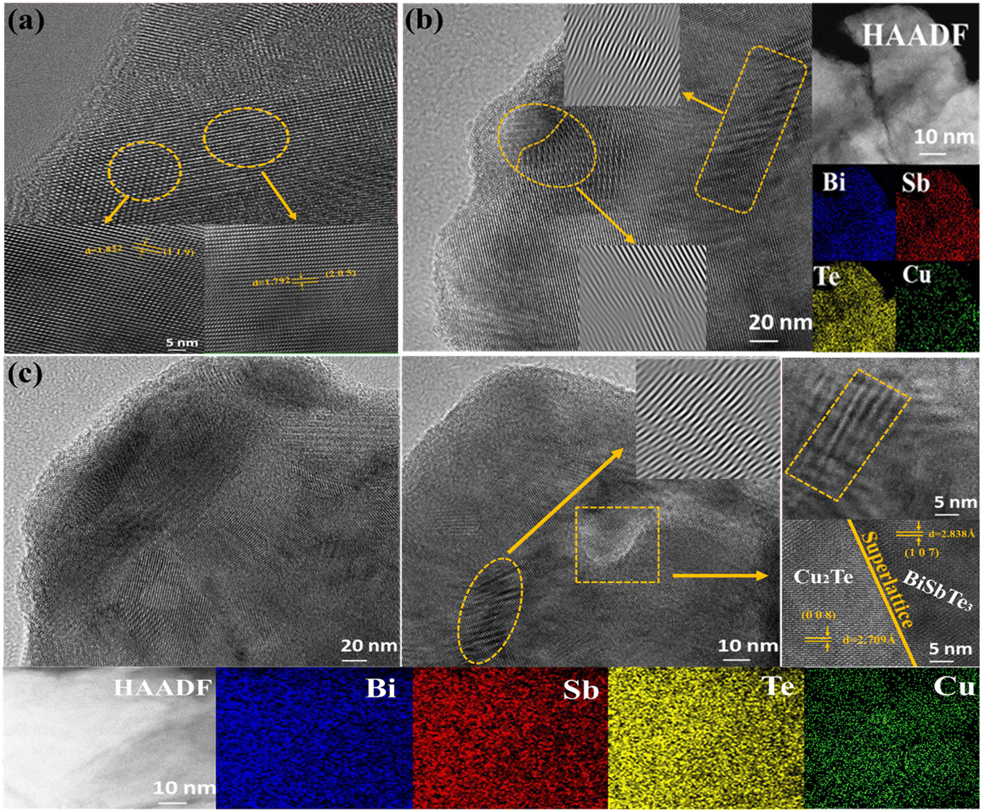 | ||
| Fig. 4 Transmission electron microscope characterization: (a) BST(KCl)3.5 sample, (b) S1 (Cu0.01Bi0.97SbTe3·KCl3.5) sample, (c) S5 (Cu0.03Bi0.97SbTe3·KCl3.5) sample. | ||
Fig. 5(a) presents the electrical transmission characteristics of Cu-doped BST samples at different temperatures. By analyzing the positive temperature-related resistivity, we observed a significant degradation in the semiconductor properties of Cu-doped samples. Experimental results demonstrate a considerable reduction in the material's resistivity after the addition of Cu. At room temperature, the minimum electrical resistivity of the material can reach 5.36 (10−6 Ω m), indicating excellent conductivity. This reduction in resistivity can be attributed to two main improvements: firstly, Cu doping plays a crucial role in modifying the microstructure of BST materials. As observed in the previous SEM analysis, the density of Cu-doped material further increases, leading to a faster and smoother electron transfer path between layers. This improved microstructure prolongs the relaxation time of the material, thereby increasing the mobility of holes in samples S1–S5 and resulting in a decrease in resistivity. Secondly, Cu doping introduces more hole carriers, increasing the free charge density in the sample and thereby improving the current conductivity. Additionally, EPMA results indicate that the incorporation of Cu further reduces the number of Te vacancies, preventing the generation of additional electrons (Te → VTe + Te(g) + 2e′). This reduction in VTe defects also weakens carrier scattering caused by defects, further improving carrier mobility. In fact, the doped samples exhibit a significant increase in hole concentration, as evidenced by the relationship between carrier concentration and temperature shown in Fig. 5(b). These additional carriers facilitate the effective transmission of electrons in the material, further reducing resistivity.
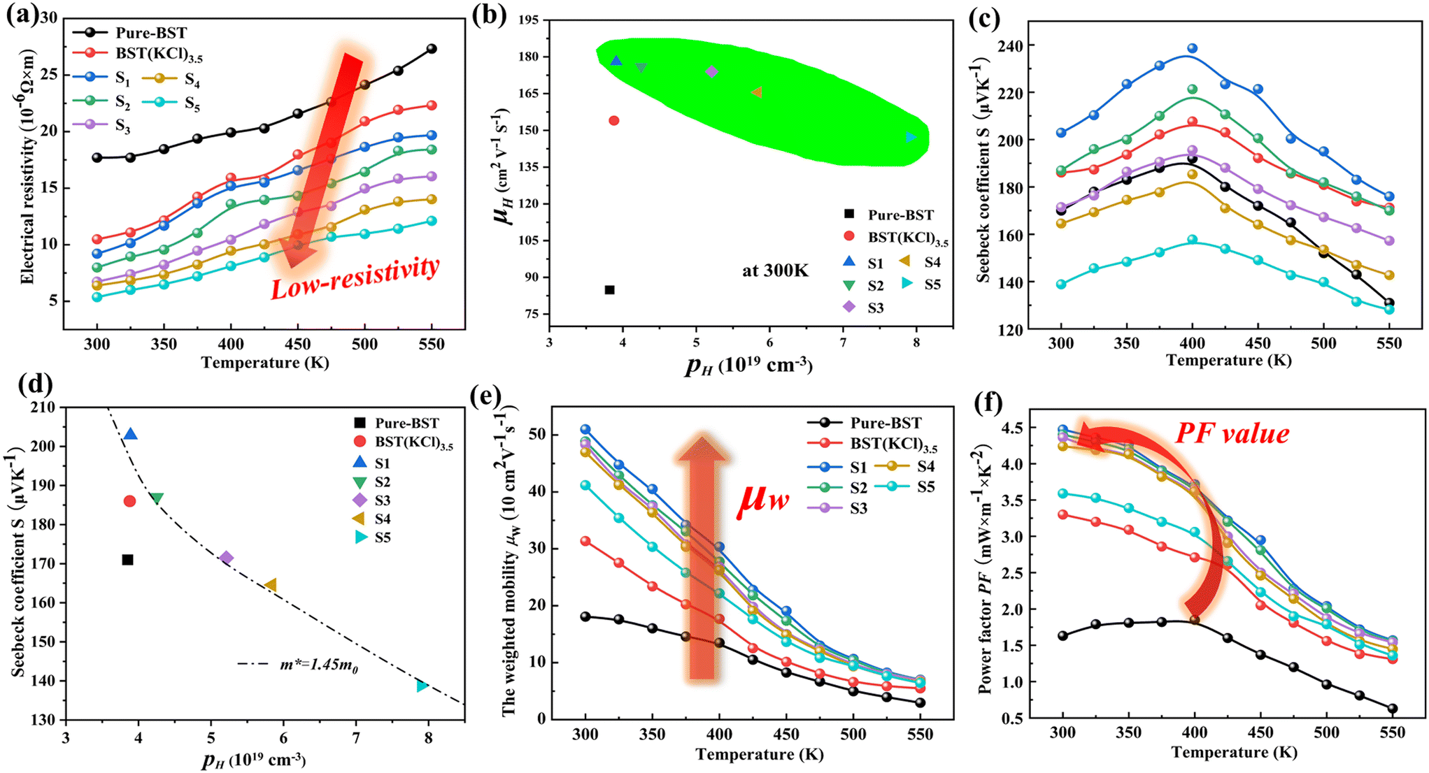 | ||
| Fig. 5 (a) Electrical resistivity for BST samples; (b) carrier concentration n and mobility μH; (c) the S values for BST samples; (d) weighted mobility μW; (e) Pisarenko plots of BST; (f) PF. | ||
By observing Fig. 5(c), we can understand the effect of Cu doping on the Seebeck coefficient. The figure illustrates that as the temperature increases, the Seebeck coefficient of the doped sample exhibits a trend of first increasing and then decreasing. It is worth noting that within the appropriate Cu doping range (0.01 < x < 0.02), the S value of the doped material shows an increase compared to the pure-BST sample. However, as the Cu doping amount further increases, the Seebeck coefficient of the BST samples gradually decreases. According to the Mott expression, the absolute value of the Seebeck coefficient strongly depends on the carrier concentration (n) and carrier mobility (μH). Therefore, the decrease in S value is mainly due to the introduction of excessive hole carriers into the BST matrix when the Cu doping amount is high.
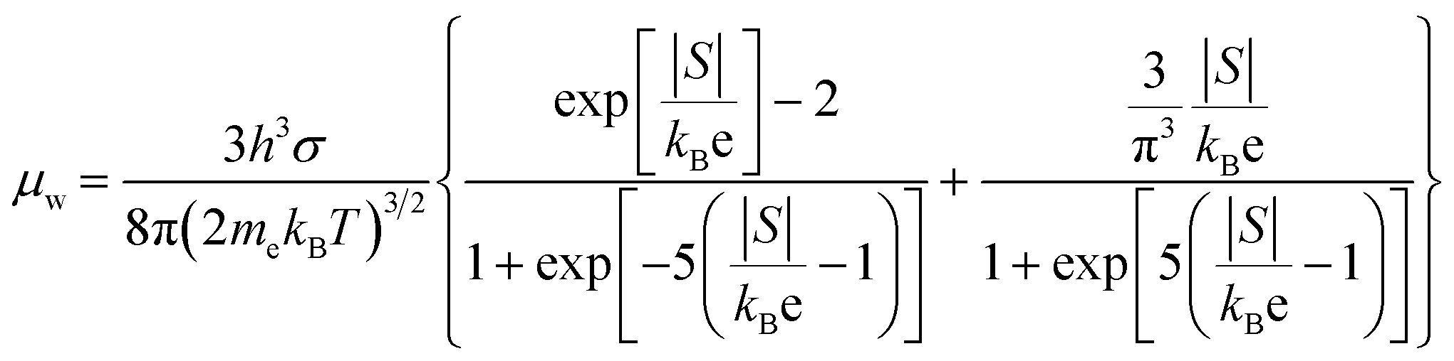
To further investigate the effect of Cu doping on the electronic structure of BST, the Pisarenko relationship between S and n at room temperature was calculated based on a single parabolic band (SPB) model (Fig. 5(d)). As shown in the figure, the S values of the S1–S4 samples are higher than those on the Pisarenko curve (m* = 1.45m0), indicating that the increase in sample S is mainly due to the increase in the effective mass of the doped material. To gain further insights into the electrical transmission characteristics of Cu-doped BST alloy samples, we introduced weighted mobility (μW), which is similar to Hall mobility (μH). It helps us understand the electronic structure and scattering characteristics in the BST matrix. The weighted mobility is calculated based on conductivity and the S-value:
 | (1) |
In the eqn (1), kB is Boltzmann's constant and h is Planck's constant. As show in Fig. 5(e), it can be observed that the μW of all BST samples within the temperature range of 300 K to 550 K decreases as the temperature increases. This phenomenon can be attributed to the presence of more grain boundaries and defects in the samples prepared using the melting method, which act as phonon scattering centers. Consequently, phonon scattering becomes the main factor influencing the carriers during the transmission process. This results in a sharp decline in the μW of the BST samples. It is noteworthy that the S1 (Cu0.01Bi0.99SbTe3(KCl)3.5) sample exhibits the highest weighted mobility among all the samples. This indicates that the addition of Cu to the sample has a positive impact on improving electron migration ability. The high weighted mobility value significantly contributes to the enhancement of the power factor (PF) in BST systems. Fig. 5(f) presents the power factor (PF value) of Cu-doped BST samples as a function of temperature. Compared with undoped samples, the PF values of Cu-doped BST alloys showed significant improvement, and sample S1 demonstrate the best performance. This enhancement can be attributed to its excellent electrical transport properties and high Seebeck coefficient. Notably, sample S1 exhibited a remarkable power factor of up to 4.47 mW m−1 K−2 at room temperature.
Fig. 6(a) shows temperature dependence of the thermal conductivity (κ) on Cu-doped samples. Within the tested temperature range, the thermal conductivity of all samples demonstrates a discernible trend in response to temperature variations. Specifically, in the range of 300 K to 400 K, the thermal conductivity gradually decreases as the temperature increases. However, once the temperature surpasses 400 K, the thermal conductivity of the material experiences a rapid increase due to the onset of the bipolar thermal diffusion effect. It is noteworthy that all Cu-doped samples exhibit higher thermal conductivity compared to the undoped samples, with the thermal conductivity of the S4 and S5 samples displaying more significant enhancements. This phenomenon can be attributed to the increased carrier concentration and improved electrical transport performance resulting from the doping process. These factors contribute to an increase in the electronic thermal conductivity of the materials (see ESI†).
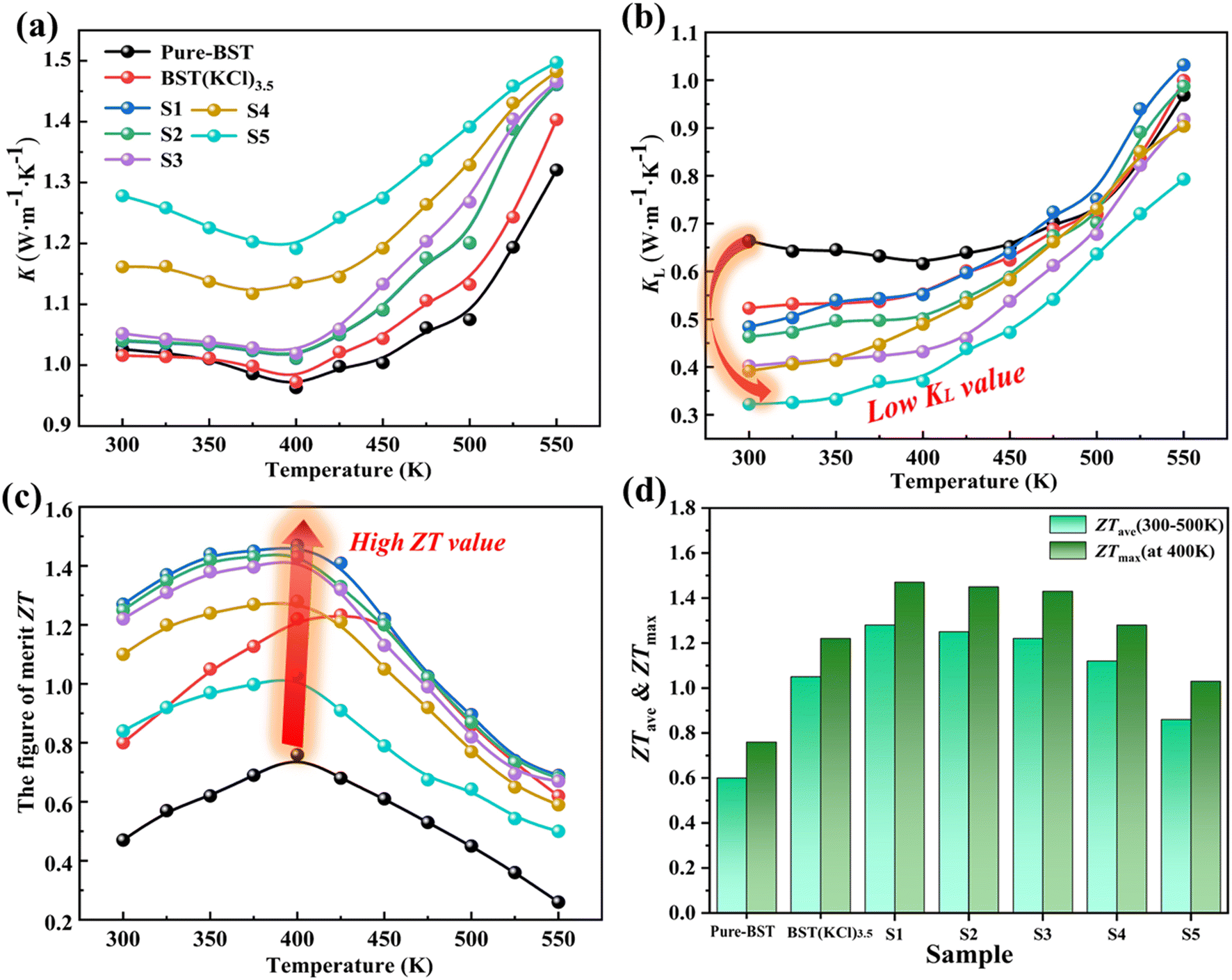 | ||
| Fig. 6 (a) Total thermal conductivity; (b) the lattice thermal conductivity; (c) ZT values; (d) ZTave & ZTmax. | ||
Based on the results presented in Fig. 6(b), it can be observed that the lattice thermal conductivity of all samples exhibits an increasing trend with temperature. However, when compared to the pure-BST, the Cu-doped samples show a significant reduction in lattice thermal conductivity. This reduction is particularly pronounced in the S5 samples with higher levels of Cu doping. The decrease in lattice thermal conductivity can be attributed to follow factors. Firstly, a large number of edge dislocations are observed in Cu-doped samples, particularly in S5 samples with high Cu doping levels. These edge dislocations effectively scatter heat transfer phonons. Additionally, in the highly doped samples, the presence of BST/Cu2Te superlattice structures further contributes to the scattering of heat transfer phonons. Finally, the addition of Cu to the BiSbTe3 system can induce changes in material quality due to the lighter mass of Cu atoms compared to the substituted Bi atoms. As a result, differences in atomic mass can alter the distribution of mass within the lattice. This fluctuation in mass distribution increases the entropy of the system, reflecting the degree of disorder. The higher entropy enhances the probability of phonon collisions, consequently, this increased phonon scattering leads to a decrease in the lattice thermal conductivity of the material. Lastly, sample S5 (Cu 0.03Bi0.97SbTe3·KCl3.5) achieved the lowest lattice thermal conductivity value of 0.32 W m−1 K−1 at 300 K.
Based on the results presented in Fig. 6(c), the variation of the dimensionless figure of merit (ZT) for all samples with temperature can be observed. The ZT values of the Cu-doped samples exhibit a significant increase across the entire temperature range. Among all samples within the measured temperature range, the S1 (Cu0.01Bi0.97SbTe3·KCl3.5) sample exhibited the highest ZT value, specifically, at room temperature, its ZT value was measured as 1.27, reaching a maximum of 1.47 at 400 K. Moreover, the average ZT value of the S1 sample within the temperature range of 300 K to 500 K was found to be 1.28. This exceptional performance can be attributed to the superior electrical and heat transfer properties of the sample. This exceptional performance can be attributed to the excellent electrical characteristics and reduced heat transfer exhibited by the sample.
4. Conclusion
The main focus of this study is to investigate the effect of Cu doping on the thermoelectric properties of BST-based alloys. Through a comprehensive analysis of electrical transmission, microstructure, and thermal performance, we obtained a series of interesting results. The experimental results show that Cu doping significantly enhances electrical properties, including increased conductivity and Seebeck coefficient. This enhancement phenomenon is due to the introduction of additional carriers after Cu doping and the improvement of effective mass. Moreover, the research focused on the microstructure of the copper-doped BST alloy, and we observed edge dislocations and BST/Cu2Te superlattice structures. These changes in the microstructure lead to a decrease in lattice thermal conductivity, further enhancing the thermoelectric properties of the material. The Cu-doped samples exhibited higher ZT values and excellent thermoelectric properties, with sample S1 exhibiting the best performance among all samples, reaching a maximum value of 1.47 at 400 K. In the temperature range of 300 K to 500 K, its average ZT value is 1.28, which remains constant within this temperature range. The improvement in performance stems from the excellent electrical properties and reduced thermal conductivity of the doped samples. The changes in microstructure and the optimization of phonon scattering mechanism jointly contribute to enhancing thermoelectric performance.Conflicts of interest
There are no conflicts to declare.Acknowledgements
This work was supported by the National Natural Science Foundation of China (Grant No. 61864012 and 21701140).References
- L. E. Bell, Science, 2008, 321, 1457–1461 CrossRef CAS PubMed.
- T. Cao, X.-L. Shi and Z.-G. Chen, Prog. Mater. Sci., 2023, 131, 101003 CrossRef CAS.
- Y. L. Chen, J.-H. Chu, J. G. Analytis, Z. K. Liu, K. Igarashi, H.-H. Kuo, X. L. Qi, S. K. Mo, R. G. Moore, D. H. Lu, M. Hashimoto, T. Sasagawa, S. C. Zhang, I. R. Fisher, Z. Hussain and Z. X. Shen, Science, 2010, 329, 659–662 CrossRef CAS.
- B. Qin and L.-D. Zhao, Science, 2022, 378, 832–833 CrossRef CAS PubMed.
- S. Roychowdhury, T. Ghosh, R. Arora, M. Samanta, L. Xie, N. K. Singh, A. Soni, J. He, U. V. Waghmare and K. Biswas, Science, 2021, 371, 722–727 CrossRef CAS PubMed.
- H. Li, Z. Xu, J. Song, H. Chai, L. Wu and L. Chen, Adv. Funct. Mater., 2022, 32, 2110047 CrossRef CAS.
- Q. D. Gibson, T. D. Manning, M. Zanella, T. Zhao, P. A. E. Murgatroyd, C. M. Robertson, L. A. H. Jones, F. McBride, R. Raval, F. Cora, B. Slater, J. B. Claridge, V. R. Dhanak, M. S. Dyer, J. Alaria and M. J. Rosseinsky, J. Am. Chem. Soc., 2020, 142, 847–856 CrossRef CAS.
- Q. D. Gibson, T. Zhao, L. M. Daniels, H. C. Walker, R. Daou, S. Hébert, M. Zanella, M. S. Dyer, J. B. Claridge, B. Slater, M. W. Gaultois, F. Corà, J. Alaria and M. J. Rosseinsky, Science, 2021, 373, 1017–1022 CrossRef CAS PubMed.
- Z. Chen, X. Zhang, J. Ren, Z. Zeng, Y. Chen, J. He, L. Chen and Y. Pei, Nat. Commun., 2021, 12, 3837 CrossRef CAS.
- S. Qu, C. Ming, P. Qiu, K. Xu, Q. Xu, Q. Yao, P. Lu, H. Zeng, X. Shi and L. Chen, Energy Environ. Sci., 2021, 14, 6586–6594 RSC.
- Z. Zhang, K. Zhao, H. Chen, Q. Ren, Z. Yue, T.-R. Wei, P. Qiu, L. Chen and X. Shi, Acta Mater., 2022, 224, 117512 CrossRef CAS.
- B. Wang, S. Zheng, Q. Wang, Z. Li, J. Li, Z. Zhang, Y. Wu, B. Zhu, S. Wang, Y. Chen, L. Chen and Z.-G. Chen, Nano Energy, 2020, 71, 104658 CrossRef CAS.
- K. Jin, J. Tiwari, T. Feng, Y. Lou and B. Xu, Nano Energy, 2022, 100, 107478 CrossRef CAS.
- F. Urbain, V. Smirnov, J.-P. Becker, A. Lambertz, F. Yang, J. Ziegler, B. Kaiser, W. Jaegermann, U. Rau and F. Finger, Energy Environ. Sci., 2016, 9, 145–154 RSC.
- C. Li, S. Ma, P. Wei, W. Zhu, X. Nie, X. Sang, Z. Sun, Q. Zhang and W. Zhao, Energy Environ. Sci., 2020, 13, 535–544 RSC.
- J. Mao, J. Iocozzia, J. Huang, K. Meng, Y. Lai and Z. Lin, Energy Environ. Sci., 2018, 11, 772–799 RSC.
- T. Zhu, R. He, S. Gong, T. Xie, P. Gorai, K. Nielsch and J. C. Grossman, Energy Environ. Sci., 2021, 14, 3559–3566 RSC.
- J. Park, M. Dylla, Y. Xia, M. Wood, G. J. Snyder and A. Jain, Nat. Commun., 2021, 12, 3425 CrossRef CAS PubMed.
- H. Jang, S. Abbey, W. H. Nam, B. Frimpong, C. V. Nguyen, S.-J. Joo, H. S. Shin, J. Y. Song, E. N. Cho, M. Kim, Y. S. Jung and M.-W. Oh, J. Mater. Chem. A, 2021, 9, 4648–4657 RSC.
- G. Wu, Z. Guo, Q. Zhang, X. Wang, L. Chen, X. Tan, P. Sun, G.-Q. Liu, B. Yu and J. Jiang, J. Mater. Chem. A, 2021, 9, 13065–13070 RSC.
- H. Hu, K. Xia, Y. Wang, C. Fu, T. Zhu and X. Zhao, J. Mater. Sci. Technol., 2021, 91, 241–250 CrossRef CAS.
- D. Yang, X. Su, J. He, Y. Yan, J. Li, H. Bai, T. Luo, Y. Liu, H. Luo, Y. Yu, J. Wu, Q. Zhang, C. Uher and X. Tang, Nat. Commun., 2021, 12, 6077 CrossRef CAS.
- Y. Zhang, Z. Li, S. Singh, A. Nozariasbmarz, W. Li, A. Genç, Y. Xia, L. Zheng, S. H. Lee, S. K. Karan, G. K. Goyal, N. Liu, S. M. Mohan, Z. Mao, A. Cabot, C. Wolverton, B. Poudel and S. Priya, Adv. Mater., 2023, 35, 2208994 CrossRef CAS PubMed.
- H. Yang, X. Huang, B. Duan, L. Wu, H. Wang, X. Feng, M. Jiang, G. Li, L. Zhou, P. Zhai and Q. Zhang, J. Mater. Sci. Technol., 2023, 144, 213–218 CrossRef CAS.
- K. Zhao, K. Liu, Z. Yue, Y. Wang, Q. Song, J. Li, M. Guan, Q. Xu, P. Qiu, H. Zhu, L. Chen and X. Shi, Adv. Mater., 2019, 31, 1903480 CrossRef CAS.
- Y. Li, J. Chen, P. Cai and Z. Wen, J. Mater. Chem. A, 2018, 6, 4948–4954 RSC.
- W. Sun, W.-D. Liu, Q. Liu and Z.-G. Chen, Chem. Eng. J., 2022, 450, 138389 CrossRef CAS.
- G. García, P. Palacios, A. Cabot and P. Wahnón, Inorg. Chem., 2018, 57, 7321–7333 CrossRef.
- J. Recatala-Gomez, A. Suwardi, I. Nandhakumar, A. Abutaha and K. Hippalgaonkar, ACS Appl. Energy Mater., 2020, 3, 2240–2257 CrossRef CAS.
- P. Acharyya, S. Roychowdhury, M. Samanta and K. Biswas, J. Am. Chem. Soc., 2020, 142, 20502–20508 CrossRef CAS.
- S. V. Barabash, V. Ozolins and C. Wolverton, Phys. Rev. B: Condens. Matter Mater. Phys., 2008, 78, 214109 CrossRef.
- C. Rudradawong, S. Khammuang, K. Kotmool, T. Bovornratanaraks, P. Limsuwan, N. Somdock, R. Sakdanuphab and A. Sakulkalavek, J. Eur. Ceram. Soc., 2023, 43, 401–406 CrossRef CAS.
- Z. Chen, X. Zhang, J. Ren, Z. Zeng, Y. Chen, J. He, L. Chen and Y. Pei, Nat. Commun., 2021, 12, 3837 CrossRef CAS PubMed.
- A. Suwardi, S. H. Lim, Y. Zheng, X. Wang, S. W. Chien, X. Y. Tan, Q. Zhu, L. M. N. Wong, J. Cao, W. Wang, Q. Yan, C. K. I. Tan and J. Xu, J. Mater. Chem. C, 2020, 8, 16940–16948 RSC.
- A. Novitskii, I. Serhiienko, S. Novikov, K. Kuskov, D. Pankratova, T. Sviridova, A. Voronin, A. Bogach, E. Skryleva, Y. Parkhomenko, A. Burkov, T. Mori and V. Khovaylo, J. Alloys Compd., 2022, 912, 165208 CrossRef CAS.
- M. Zhang, X. Tang, N. Li, G. Wang, G. Wang, A. Liu, X. Lu and X. Zhou, Appl. Phys. Lett., 2020, 116, 173902 CrossRef CAS.
- X. Li, H. Yu, S. Gao, X. Fan, D. Zhou, W. Ji, Y. Chen, Y. Zhang, H. Ma and X. Jia, Mater. Charact., 2023, 199, 112792 CrossRef CAS.
- F. M. El-Makaty, M. Nawaz, R. A. Shakoor, A. Hammuda and K. M. Youssef, Mater. Charact., 2023, 202, 112987 CrossRef CAS.
- P. Wyżga, S. Grimm, V. Garbe, E. Zuñiga-Puelles, C. Himcinschi, I. Veremchuk, A. Leithe-Jasper and R. Gumeniuk, J. Mater. Chem. C, 2021, 9, 4008–4019 RSC.
- P. Kayser, F. Serrano-Sanchez, O. J. Dura, F. Fauth and J. A. Alonso, J. Mater. Chem. C, 2020, 8, 5509–5516 RSC.
- P. Kayser, F. Serrano-Sanchez, O. J. Dura, F. Fauth and J. A. Alonso, J. Mater. Chem. C, 2020, 8, 5509–5516 RSC.
- Y. Wang, Y. Song, K. Song, L. Pan, C. Chen, K. Koumoto and Q. Liu, J. Mater. Sci. Technol., 2022, 117, 251–258 CrossRef CAS.
- T. Cao, X.-L. Shi and Z.-G. Chen, Prog. Mater. Sci., 2023, 131, 101003 CrossRef CAS.
- H. He, X. Lu, E. Hanc, C. Chen, H. Zhang and L. Lu, J. Mater. Chem. C, 2020, 8, 1494–1516 RSC.
- C. Tan, X. Tan, B. Yu, G.-Q. Liu, H. Wang, G. Luo, J. Xu, Q. Wu, B. Liang and J. Jiang, ACS Appl. Energy Mater., 2019, 2, 6714–6719 CrossRef CAS.
- H.-J. Wu and W.-T. Yen, Acta Mater., 2018, 157, 33–41 CrossRef CAS.
- Y. S. Lim, M. Song, S. Lee, T.-H. An, C. Park and W.-S. Seo, J. Alloys Compd., 2016, 687, 320–325 CrossRef CAS.
Footnote |
| † Electronic supplementary information (ESI) available: Experimental thermal diffusivity and specific heat capacity details. The detailed material preparation process. See DOI: https://doi.org/10.1039/d3ce00951c |
| This journal is © The Royal Society of Chemistry 2024 |