
Bright colloidal gallium-doped CuInS2 quantum dots for luminescent solar concentrators†
Haoran
Chen
a,
Zhipeng
Xu
a,
Zhijun
Shi
a,
Fenghuan
Zhao
b,
Lixin
Cao
a,
Bohua
Dong
 *a and
Chenghui
Xia
*a
*a and
Chenghui
Xia
*a
aSchool of Materials Science and Engineering, Ocean University of China, No. 1299, Sansha Road, West Coast New District, Qingdao, 266404, P. R. China. E-mail: dongbohua@ouc.edu.cn; c.xia@ouc.edu.cn
bDepartment of Mechanical and Electrical Engineering, Rizhao Polytechnic, 16 Yantai North Road, Rizhao City, Shandong Province, P. R. China
First published on 14th November 2024
Abstract
We have developed an efficient strategy to improve the brightness and stability of CuInS2 quantum dots via Ga3+ doping combined with the overgrowth of a ZnS shell. The incorporation of Ga3+ into crystal lattices greatly suppresses the diffusion of Cu+ and reduces the formation of Cu-related defects, leading to a photoluminescence quantum yield as high as 92%. These nanocrystals can be integrated into luminescent solar concentrators and the devices exhibit a power conversion efficiency reaching 3.87%.
Luminescent solar concentrators (LSCs) are of great interest in distributed photovoltaic power generation due to their ability to be integrated into the building envelope as windows or facades.1–5 Typically, LSCs consist of a waveguide medium containing bright luminophores that absorb incident light, and guide and concentrate the low energy emission light to a photovoltaic cell for solar energy conversion. To date, numerous luminophores, such as organic dyes, rare earths, and quantum dots (QDs) have been widely applied in the fabrication of LSC devices.1 Among them, luminescent QDs have been considered ideal candidates due to their great flexibility in tuning absorption and photoluminescence (PL) spectra, low self-absorption and excellent stability.1–3 However, the majority of reported QDs are limited to Cd-based nanocrystals, which are strictly forbidden for use in daily life due to their high toxicity.
Colloidal CuInS2 quantum dots have attracted increasing attention in LSCs due to their large absorption coefficients across a broad spectral range, size- and composition-tunable PL from the visible to the near-infrared (NIR) region with large Stokes shift, and low toxicity in nature.6–11 In 2015, Klimov and co-authors reported the use of CuInSxSe2−x/ZnS QDs in LSCs with an optical efficiency of 3.27%.6 As the PL spectra of these QDs are rather broad, some of the low energy emitting photons (>0.8 eV) cannot be efficiently absorbed and converted into electricity while using silicon solar cells as the assembly unit of LSCs. To overcome this issue, Gamelin and co-authors synthesized a batch of CuInS2/CdS QDs with an emission wavelength centred at ∼780 nm where the emission perfectly overlaps with the solar-cell external quantum efficiency spectrum.7 The fabricated LSC shows a broad solar absorption, high PL quantum yields (PLQYs) and moderate reabsorption losses, leading to exceptionally high projected flux gains for planar LSCs coupled to Si photovoltaics. Later studies of CuInS2 applied in LSCs have been widely spread across the academic community and the architectures are no longer limited to single planar waveguide structures. Several new types of LSCs have also been reported, such as tandem LSCs,10 sandwich LSCs,8 multiple-interlayer LSCs,11 and even liquid LSCs.12
Nevertheless, the power conversion efficiency (PCE) of CuInS2-based LSCs remains to be less than 3.7%.11,12 The realization of their full potential is mainly hindered by their underdeveloped synthesis due to the difficulty in balancing the reactivities of multiple precursors and the high solid-state diffusion rates of Cu+ in the crystal lattice.13 Theoretical calculation proves that the Cu self-diffusion coefficient (2.2 × 10⁻⁶ cm−2 s−1) in chalcocite is about 10 times larger than that in water.14,15 This characteristic makes it extremely easy to intrinsically generate Cu-related defects that are deleterious to the PLQYs and stability.
In this work, we propose an efficient strategy to improve the brightness and stability of CuInS2 QDs via high valent Ga3+ doping in CuInS2 cores followed by epitaxial overgrowth of a ZnS shell. Theoretical modelling confirms that the incorporation of Ga3+ into CuInS2 crystal lattices greatly suppresses the diffusion of Cu+ and thus to a large extent reduces the formation of Cu-related defects. The product QDs can exhibit PLQYs as high as 92% and they can be applied in LSCs with a PCE reaching 3.87%.
Ternary CuInS2 QDs were synthesized using a one-pot heating up method and the resulting crude nanocrystals were further used as cores for Ga3+ doping at 120 °C, followed by slow injection of ZnS precursors at 220 °C for 10 h (see Methods in the ESI†). X-ray diffraction (XRD) patterns in Fig. 1a show that the CuInS2 QDs have a tetragonal chalcopyrite structure with a crystallinity of 85.2% (Fig. S1 and Table S1, ESI†). The average crystalline size estimated from the XRD patterns using the Scherrer equation is 2.7 nm. After Ga3+ doping, the crystallite size of yielded QDs decreases to 2.5 nm accompanied by a subtle shift to high angles in the XRD patterns. The decrease in QD sizes after Ga-doping (from 3.2 to 2.9 nm) is also observed in the transmission electron microscopy (TEM) images shown in Fig. S2a and b (ESI†). These interesting findings may be due to the incorporation of a smaller ionic radius of Ga3+ (62 pm) with respect to the host Cu+ (96 pm) and In3+ (81 pm) into anionic sublattices, leading to a slight shrinkage of crystal lattices. With the subsequent ZnS shelling on pure CIS and Ga-doped CIS QDs (CIGS), the crystallite size of the resulting products increases to 4.2 nm and they retain their tetragonal chalcopyrite crystal structure. The diffraction peaks also shift to high angles. This is possibly due to the decrease of lattice spacing either by the incorporation of a smaller ionic radius of Ga3+ (62 pm) and Zn2+ (74 pm) or lattice stress caused by the ZnS layer, or both.
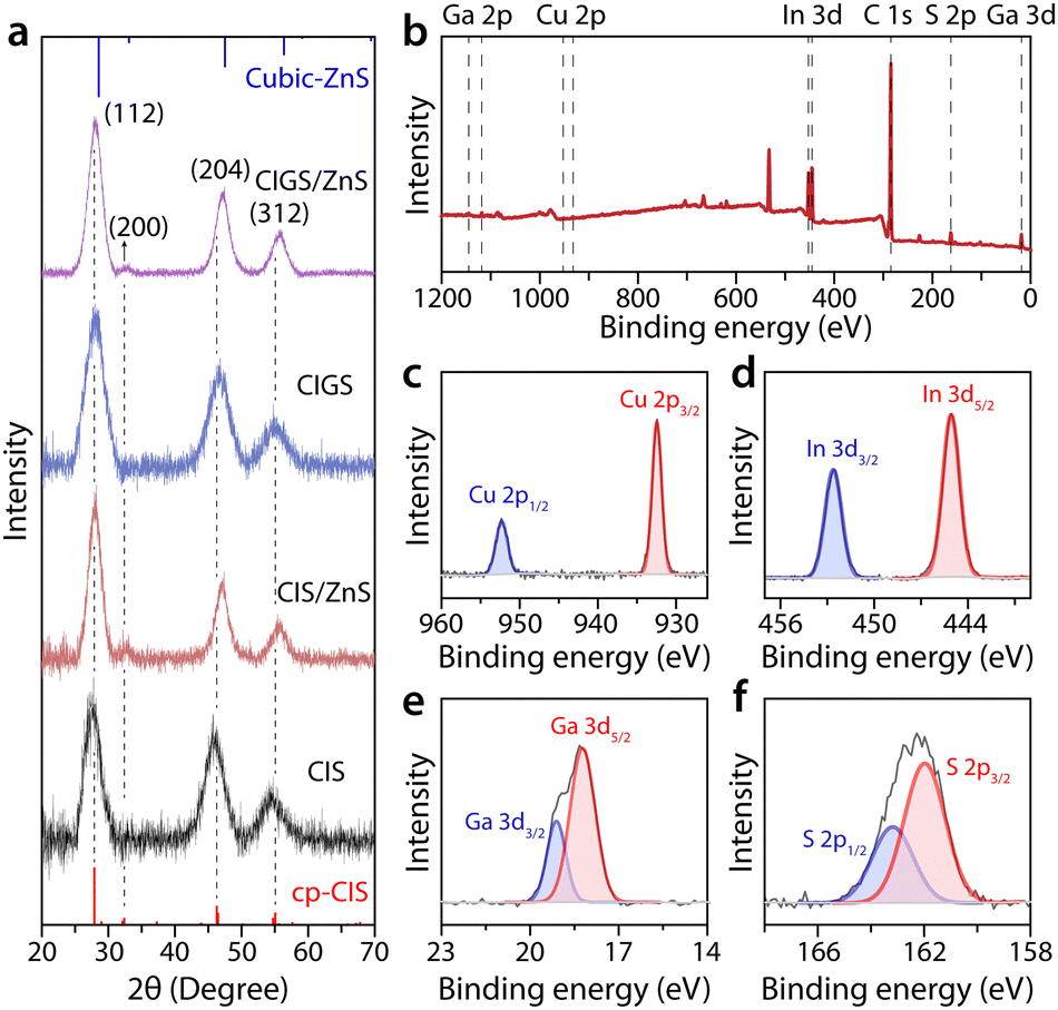 | ||
| Fig. 1 (a) XRD patterns of CIS and CIGS QDs before and after ZnS shelling. The red vertical lines on the bottom frame and the blue vertical lines on the top frame represent the tetragonal chalcopyrite CIS and cubic ZnS, respectively. (b) XPS survey spectrum of the purified CIGS QDs with assignment of the observed peaks (top panel). (c)–(f) High resolution XPS spectra of Cu, In, Ga and S in purified CIGS QDs. | ||
To verify the successful doping of gallium in CuInS2, X-ray photoelectron spectroscopy (XPS) was performed on the Ga-doped CuInS2 QDs. The XPS survey spectrum and high resolution XPS spectra of relevant elements are shown in Fig. 1b–f. The binding energy peaks at 932.1 eV and 951.9 eV can be indexed to Cu 2p3/2 and Cu 2p1/2 of Cu(I) in CuInS2 QDs, respectively. The absence of satellite features around 942 eV confirms that no Cu2+ exists in the product samples. The two intense peaks at 444.3 eV and 451.9 eV are ascribed to the binding energies of In 3d5/2 and 3d3/2 of indium(III), while overlapped peaks centred at 161.8 eV and 163.1 eV can be attributed to the binding energies of S 2p3/2 and S 2p1/2 of S(II) in CuInS2 QDs. Taking a closer look at the binding energy around 18 eV, non-negligible and asymmetric peaks ascribed to the binding energies of Ga 3d of gallium(III) can be observed. This observation confirms the incorporation of Ga3+ into CuInS2 QDs. Inductively coupled plasma optical emission spectroscopy measurements also confirm the existence of Ga3+ in the resulting QDs and the composition can be written as Cu1.17In1.06Ga0.16S2 (ESI† Fig. S3).
The absorption and PL spectra of the CIS and CIGS QDs before and after ZnS shelling are presented in Fig. 2a. They exhibit featureless absorption across a broad spectral range. The first absorption transition energies are determined by seeking the minima of the second derivatives of the absorption spectra. Those values are used to deduce the average sizes of the CIS QDs according to the previously reported methods (see details in supporting method 1, ESI† Fig. S4 and Table S2).16 Calculations show that the CIS and CIGS QDs have sizes of 2.56 nm and 2.53 nm, which agree well with the sizes extracted from the XRD patterns and TEM images (ESI† Table S1 and Fig. S2a,b).
 | ||
| Fig. 2 (a) Absorption and PL spectra of CIS and CIGS QDs before and after ZnS shelling. (b) PL spectra of CIGS QDs with different Ga/Cu feeding ratios. | ||
As shown in Fig. 2a, the incorporation of Ga3+ into CIS QDs leads to a slight blue-shift in both absorption and PL spectra. The blue shifts become more intense while increasing the feeding ratios of Ga/Cu from 1 to 8 (Fig. 2b). This phenomenon has also been observed in the previous literature and can be explained by an increase of band gaps due to a smaller effective CIS core size, as verified by the size estimation from the XRD patterns (the size shrinks from 2.7 to 2.5 nm), TEM images (the size shrinks from 3.2 to 2.9 nm) and absorption spectra (the size shrinks from 2.56 to 2.53 nm) of CIS and CIGS QDs shown in Fig. 1a, 2a and Fig. S2a,b (ESI†). The increase of band gaps also can be attributed to the formation of wider band gap CIGS alloys during the reaction, as the band gap of bulk CuGaS2 is larger than that of CIS (2.5 and 1.55 eV, respectively).13 As shown in Fig. 2a, the spectral shifts are further strengthened after ZnS shelling both on CIS and CIGS QDs. This is likely due to the Cu+ or In3+ for Zn2+ cation exchange followed by Zn2+ interdiffusion in crystal lattices, leading to shrinkage of effective core sizes or formation of wide band gap alloyed structures.17–20 Despite the size or composition changes in CIS cores, the sizes of CIS and CIGS QDs after ZnS shelling increase from 3.2 and 2.9 nm to 4.3 and 3.6 nm respectively, indicating the successful overgrowth of the ZnS layer (ESI,† Fig. S2c and d).
We notice that the PL quantum yields (PLQYs, supporting method 2, Fig. S5, ESI†) of the resulting CIGS QDs increase from 12 to 17% with respect to that of the CIS QDs and the value even goes up to 92% after ZnS shelling. The extent of enhancement in PLQYs is much larger than that of the CIS/ZnS QDs (∼56%), suggesting that Ga3+ plays an important role in the exciton recombination process. Such a significant increase in PLQYs could stem from a strong improvement in radiative recombination rates or the elimination of nonradiative recombination pathways, or both.21 Indeed, the average PL lifetimes of CIGS and CIGS/ZnS are generally longer than those of CIS and CIS/ZnS QDs, respectively (Fig. S6, ESI†). In addition, the CIGS/ZnS QDs exhibit better photostability than the CIS/ZnS QDs and some other CIS/ZnS QDs as well as CsPbBr3 prepared according to the recent literature (Fig. S7, ESI†).22,23 Previous reports proposed that the enhancement of PLQYs is due to the passivation of nonradiative recombination centers at the surface.17–20 Given that the enhancement of PLQYs is solely due to the surface passivation, the PLQYs and average lifetimes of CIGS/ZnS QDs should be comparable with those of CIS/ZnS QDs since the cores are coated by ZnS under the same circumstance, which is however not the case. This great discrepancy implies that the incorporation of Ga3+ into CIS QDs not only removes the surface defects but also likely reduces the defects deeply located in the crystal lattice by the Cu+ or In3+ for Ga3+ cation exchange.
To validate this hypothesis, the doping concentration of Ga3+ was tuned by increasing the feeding amount of gallium precursors during the cation exchange reactions. As shown in Fig. 2b, the PL spectra gradually shift to high energies, implying that an increased amount of Ga3+ has been successfully doped into crystal lattices. The gradual introduction of Ga3+ (Ga/Cu ≤4) into crystal lattices is indeed beneficial for the enhancement of their PLQYs (from 12 to 23%). Overload of Ga3+ however deteriorates the luminescence and it is possibly related to the formation of new defect states in the nanocrystals, such as interstitial atoms (Gai) and substitutional impurities (GaCu, GaIn). Due to various possibilities in compositions and the scarce literature on the PL of CIGS QDs, it would be difficult to unambiguously identify the radiative recombination mechanism in these materials. Nevertheless, the great enhancement of PLQYs after the introduction of a small amount of Ga3+ suggests that Ga-doping possibly prohibits the formation of defects not only on the surface but also in crystal lattices. According to the previous reports, Cu atoms exhibit a high diffusion rate (2.2 × 10⁻⁶ cm−2 s−1) in chalcocite Cu2S.14,15 This characteristic makes it extremely easy to intrinsically generate Cu-related defects that are deleterious to the PLQYs and stability. We thus speculate that the incorporation of Ga3+ into CIS QDs may restrict the random diffusion of Cu+ in crystal lattices, therefore leading to an increase in PLQYs.
We next carried out density functional theory calculations to estimate the diffusion coefficient of Cu+ both in the tetragonal chalcopyrite CIS and Ga-doping CIS QDs (see supporting method 3 for calculation details ESI†). Fig. 3a shows the Cu atom which diffuses the longest distance at 290 K in the simulation. The trajectory shows that the Cu atoms diffuse continuously from one site to another much like in a liquid. The average diffusion distance squares as functions of time for the chalcopyrite CIS and Ga-doped CIS QDs are presented in Fig. 3b. We can see that the average distance square for Cu atoms grows linearly with time, following a typical random diffusion picture. The Cu self-diffusion coefficient for the CIGS QDs is 0.55 × 10⁻⁶ cm−2 s−1, which is only one-third of that for the pure CIS QDs (1.75 × 10⁻⁶ cm−2 s−1). Interestingly, we notice that the values are smaller than that for Cu in Cu2S crystals (2.2 × 10⁻⁶ cm−2 s−1).14 The trends of Cu diffusion coefficients in Cu2S, CIS, and CIGS clearly show that the Cu diffusion barrier increases along with the incorporation of high valent cations. Along with the incorporation of Ga3+ into CIS QDs, the diffusion rate of Cu+ is greatly limited, thus resulting in fewer defects in crystal lattices. Consequently, the stabilized structure enables CIGS QDs to maintain better luminescent performance both before and after ZnS shelling.
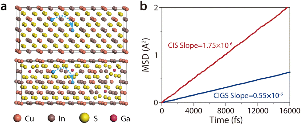 | ||
| Fig. 3 (a) Simulated cell of CIS QDs and Ga-doped CIS QDs with S atoms denoted by yellow balls, Cu by orange balls, In by grey balls, Ga by pink balls and the longest diffusing Cu atoms by cyan balls. Its initial and final positions are connected by a dashed line. (b) Average diffusion distance squares of Cu+ in CIS and Ga-doped CIS crystal lattices as functions of time at 290 K. | ||
The bright CIGS/ZnS QDs (PL peak at 585 nm, 0.1 wt%) were then embedded into poly(methyl methacrylate) and the single planar waveguides were cut and polished to 5 cm × 5 cm × 0.5 cm LSC devices (named as LSC#1, see method section for details ESI†). As shown in Fig. 4a, LSC#1 exhibits a good transmittance reaching over 70% at a wavelength longer than 600 nm. The PL spectrum of LSC#1 was acquired on the edge of the device and a clear red shift (∼30 nm) was observed with respect to the QDs in solution. This is possibly due to the aggregation of QDs during the bulk polymerization of methyl methacrylate. The planar LSC#1 was then coupled to a commercial silicon cell (with a PCE of 12.5%) and the PCE was evaluated using a solar cell IV test system according to the previously reported procedures.24,25 As shown in Fig. 4b, LSC#1 exhibits a short current density of 6.64 mA cm−2, an open-circuit voltage of 0.51 V with a fill factor of 0.71, and a PCE reaching 2.41%, comparable with the previously reported values.6–12 To investigate the effect of emission wavelength on the LSC performance, a new batch of CIGS/ZnS QDs with emission peaks at 685 nm were prepared by tuning the size of CIS cores. The QDs were fabricated into LSC devices (LSC#2) using the same procedures. The newly prepared LSC#2 also exhibits excellent transmittance and the PCE is further improved to 2.67%.
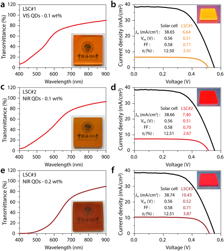 | ||
| Fig. 4 (a), (c) and (e) Transmission spectra of LSCs with different types and concentrations of QDs. Insets show the planar LSCs under ambient light. (b) and (d) and (f) I–V curves of the as-prepared LSC prototypes (5 × 5 × 0.5 cm) and the coupled silicon cells. They were measured with a sunlight simulator under AM1.5 illumination. Insets show the digital images of LSCs under 365 nm UV light. | ||
It can be seen that the LSC devices based on NIR-emitting CIGS/ZnS QDs exhibit excellent performance in terms of both PCE and transmittance. This is likely attributed to the fact that the NIR-emitting QDs exhibit small reabsorption and their PL spectra are matched well to the response curve of the photovoltaic cell at the edge of the device, as discussed in ESI† Fig. S8. We further applied twice the mass fraction (0.2 wt%) of NIR-emitting CIGS/ZnS QDs in the LSC and found that the PCE of the LSC was as high as 3.87% while guaranteeing high transmittance (Fig. 4e and f). Continuously increasing the QD concentration (0.4 wt%) leads to a slight increase of PCE up to 4.15% and a sharp decrease of device transparency across the whole visible and even NIR spectral range (Fig. S9, ESI†). The PCE is not enhanced proportionally which can be due to increased reabsorption or inevitable aggregation of QDs at a rather high concentration during the polymerization process as indicated by the red-shift in PL spectra (Fig. S10, ESI†).
In conclusion, we have developed an efficient strategy to improve the brightness and stability of CuInS2 QDs via Ga3+ doping combined with the overgrowth of a ZnS shell. The incorporation of Ga3+ into crystal lattices greatly suppresses the diffusion of Cu+ and reduces the formation of Cu-related defects, leading to PLQYs as high as 92%. These QDs can be integrated into LSCs and the devices exhibit a PCE reaching 3.87%, being of great potential for distributed photovoltaic power generation.
C. X. acknowledges the financial support from the Taishan Scholar Project of Shandong Province (Grant no.: tsqn202306113), the Excellent Youth Science Fund Project Shandong Province (Grant no.: 2024HWYQ-037), the Natural Science Foundation of Shandong Province (Grant no.: ZR2023QB174), the China Postdoctoral Science Foundation (Grant no.: 2023M733328), the Natural Science Foundation of Qingdao (Grant no.: 23-2-1-82-zyyd-jch), and the Postdoctoral Science Foundation of Qingdao (Grant no.: QDBSH20230201024).
Data availability
The data supporting this article have been included as part of the ESI.†Conflicts of interest
There are no conflicts to declare.References
- F. Meinardi, F. Bruni and S. Brovelli, Nat. Rev. Mater., 2017, 2, 17072 CrossRef CAS.
- L. R. Bradshaw, K. E. Knowles, S. McDowall and D. R. Gamelin, Nano Lett., 2015, 15, 1315–1323 CrossRef CAS PubMed.
- F. P. G. d Arquer, D. V. Talapin, V. I. Klimov, Y. Arakawa, M. Bayer and E. H. Sargent, Science, 2021, 373, eaaz8541 CrossRef PubMed.
- I. Papakonstantinou, M. Portnoi and M. G. Debije, Adv. Energy Mater., 2021, 11, 2002883 CrossRef CAS.
- S. Castelletto and A. Boretti, Nano Energy, 2023, 109, 108269 CrossRef CAS.
- F. Meinardi, H. McDaniel, F. Carulli, A. Colombo, K. A. Velizhanin, N. S. Makarov, R. Simonutti, V. I. Klimov and S. Brovelli, Nat. Nanotechnol., 2015, 10, 878–885 CrossRef CAS PubMed.
- K. E. Knowles, T. B. Kilburn, D. G. Alzate, S. McDowall and D. R. Gamelin, Chem. Commun., 2015, 51, 9129–9132 RSC.
- M. R. Bergren, N. S. Makarov, K. Ramasamy, A. Jackson, R. Guglielmetti and H. McDaniel, ACS Energy Lett., 2018, 3, 520–525 CrossRef CAS.
- R. Sumner, S. Eiselt, T. B. Kilburn, C. Erickson, B. Carlson, D. R. Gamelin, S. McDowall and D. L. Patrick, J. Phys. Chem. C, 2017, 121, 3252–3260 CrossRef CAS.
- K. Wu, H. Li and V. I. Klimov, Nat. Photonics, 2018, 12, 105–110 CrossRef CAS.
- A. R. M. Velarde, E. R. Bartlett, N. S. Makarov, C. Castañeda, A. Jackson, K. Ramasamy, M. R. Bergren and H. McDaniel, ACS Appl. Energy Mater., 2020, 3, 8159–8163 CrossRef CAS.
- X. Liu, B. Luo, J. Liu, D. Jing, D. Benetti and F. Rosei, J. Mater. Chem. A, 2020, 8, 1787–1798 RSC.
- A. C. Berends, M. J. J. Mangnus, C. Xia, F. T. Rabouw and C. de Mello Donega, J. Phys. Chem. Lett., 2019, 10, 1600–1616 CrossRef CAS PubMed.
- L.-W. Wang, Phys. Rev. Lett., 2012, 108, 085703 CrossRef PubMed.
- J. Wang, J. Gao, M.-Y. Chou and U. Landman, Nano Lett., 2021, 21, 8895–8900 CrossRef CAS PubMed.
- C. Xia, W. Wu, T. Yu, X. Xie, C. van Oversteeg, H. C. Gerritsen and C. de Mello Donega, ACS Nano, 2018, 12, 8350–8361 CrossRef CAS PubMed.
- L. Li, A. Pandey, D. J. Werder, B. P. Khanal, J. M. Pietryga and V. I. Klimov, J. Am. Chem. Soc., 2011, 133, 1176–1179 CrossRef CAS PubMed.
- C. Xia, J. D. Meeldijk, H. C. Gerritsen and C. de Mello Donegá, Chem. Mater., 2017, 29, 4940–4951 CrossRef CAS PubMed.
- L. De Trizio, M. Prato, A. Genovese, A. Casu, M. Povia, R. Simonutti, M. J. P. Alcocer, C. D’Andrea, F. Tassone and L. Manna, Chem. Mater., 2012, 24, 2400–2406 CrossRef CAS.
- J. Park and S.-W. Kim, J. Mater. Chem., 2011, 21, 3745–3750 RSC.
- S. O. M. Hinterding, A. C. Berends, M. Kurttepeli, M.-E. Moret, J. D. Meeldijk, S. Bals, W. van der Stam and C. de Mello Donega, ACS Nano, 2019, 13, 12880–12893 CrossRef CAS PubMed.
- Z. Liu, C. Hao, Y. Sun, J. Wang, L. Dube, M. Chen, W. Dang, J. Hu, X. Li and O. Chen, Nano Lett., 2024, 24, 5342–5350 CrossRef CAS PubMed.
- M. D’Amato, L. Belzane, C. Dabard, M. Silly, G. Patriarche, Q. Glorieux, H. Le Jeannic, E. Lhuillier and A. Bramati, Nano Lett., 2023, 23, 10228–10235 CrossRef PubMed.
- C. Yang, D. Liu and R. R. Lunt, Joule, 2019, 3, 2871–2876 CrossRef.
- M. G. Debije, R. C. Evans and G. Griffini, Energy Environ. Sci., 2021, 14, 293–301 RSC.
Footnote |
| † Electronic supplementary information (ESI) available: Experimental details, theoretical modelling details, XRD patterns and the corresponding analysis, PL spectra and decay curves. See DOI: https://doi.org/10.1039/d4cc05375c |
| This journal is © The Royal Society of Chemistry 2024 |