
 Open Access Article
 This Open Access Article is licensed under a
 Creative Commons Attribution 3.0 Unported Licence
Visualizing nanoscale heterogeneity in perylene thin films via tip-enhanced photoluminescence with unsupervised machine learning†
Pavel
Valencia-Acuna
a,
Kushal
Rijal
b,
Chih-Feng
Wang
 a,
Maxim
Ziatdinov
a,
Wai-Lun
Chan
*b and
Patrick Z.
El-Khoury
*a
a,
Maxim
Ziatdinov
a,
Wai-Lun
Chan
*b and
Patrick Z.
El-Khoury
*a
aPhysical Sciences Division, Pacific Northwest National Laboratory, Richland, WA 99352, USA. E-mail: patrick.elkhoury@pnnl.gov
bDepartment of Physics and Astronomy, The University of Kansas, Lawrence, KS 66045, USA. E-mail: wlchan@ku.edu
First published on 24th June 2024
Abstract
We investigate the properties of ultrathin 3,4,9,10-perylenetetracarboxylic diimide (PTCDI) films using a combination of tip-enhanced photoluminescence and unsupervised machine learning. We expose nanoscale spectral heterogeneities that can be understood on the basis of the interplay between vibronic effects, intermolecular excitons, and intramolecular excitons in PTDCI films.
Organic semiconductors have been a focal point in modern optoelectronics research.1–3 Indeed, as a result of their unique properties and reduced dimensions, molecular nano-films have been used as key sub-components in transistors,4 solar cells,5 and light emitting diodes.6 In this context, the rational design of efficient miniaturized devices that harness the full power of these ultrathin molecular semiconductors requires a detailed molecular-level understanding of structure–property relationships in these structures. Although many studies have investigated how the average (macroscopic) morphology of organic thin films correlates with device performance,7–9 impacts from the spatial variations in the local morphology and properties are less clear.
Many important processes such as light emission, carrier recombination, or charge separation may preferentially occur at “hotspots” in organic films. Hence, site-specific properties rather than the large area averaged properties are important to study. Recent advances in nanooptics and nanophotonics are promising in this regard. Specifically, the two now fairly widespread techniques of tip-enhanced Raman scattering (TERS)10 and tip-enhanced photoluminescence (TEPL)11,12 can provide detailed insights into the vibrational and electronic properties of molecular and materials systems. Sequential or even simultaneously recorded topographic maps may also be readily used to inspect correlations between structure and optical properties on the nanoscale. Even though TERS and TEPL have been amply used to characterize molecular and materials systems,13–18 these techniques have not been thoroughly explored within nanometer-scale organic semiconductor research, specifically in exciton-supporting molecular thin films. This is the topic of this work.
As mentioned above, the origins of light emission from organic semiconductors have been previously explored using conventional spectroscopic and microscopic approaches.17–19 The previously employed methods are however limited by diffraction to spatial resolutions on the order of a few hundred nanometers with driving sources in the visible-near IR region of the spectrum. In the case of perylene films, the subject of this work, the recorded PL spectra exhibit a complex multi-peak structure that arises from the recombination of intramolecular and intermolecular excitons, with contributions from vibronic sub-bands.20 Indeed, this kind of complex PL spectrum is quite common in molecular aggregates. The strong intermolecular electronic coupling along the p-stacking direction can produce both intramolecular excitons and intermolecular charge transfer excitons,21 while electronic–vibrational interactions yield red-shifted vibronic sub-bands.22 Both of these effects and the resultant optical spectra depend strongly on the molecular packing within the aggregate. One of the motivations behind the present work is to understand the interplay between the different emission channels and the underlying molecular arrangements that drive them on the nanometer length scales. We use a 2 nm thick PTCDI film on gold (Au)23 as a prototypical system in our current study. Prior to an exposition of our results, it is important to mention that our TEPL measurement protocol is very well described in recent work to which the reader is referred.12 The conditions used here are otherwise described in figure captions and the main text, as needed.
Fig. 1a displays a topographic AFM map of a 2 nm-thick PTCDI film on Au, which was recorded using tapping mode feedback. The 2 nm film was thermally deposited in an ultra-high vacuum chamber at a very slow rate (0.03 nm minute−1). From our previous experience,24,25 ultrathin films deposited on a metal surface at this condition are typically continuous because of strong molecule–substrate interactions. The energy level diagram of the PTCDI/Au interface is shown in the inset of Fig. 1a. This diagram is drawn based on the ultraviolet photoemission spectroscopy (UPS) measurements (Fig. S1, ESI†), which are discussed in more detail in the ESI.† PTCDI is an n-doped semiconductor and excited electrons in PTCDI can be transferred readily to the Au substrate based on the band alignment. The grains observed in the height map arise from PTDCI aggregates, which cover the whole substrate with the exception of a few areas that appear as dark nano-holes in the AFM map. Nano-optical measurements were performed using a silver (Ag)-coated silicon tip irradiated using a 532 nm laser source. As schematically illustrated in Fig. 1b, unlike the case of topographic mapping, an intermittent contact mode was used for TEPL mapping. Namely, two spectra are recorded at every pixel of the spectral nano-images. The first signals were recorded when the tip is 30–40 nm away from the sample (Fig. 1c), whereas the second set of signals were obtained when the tip is in contact with the substrate (Fig. 1d). In this scheme, the far field response (tip out) is dominated by scattering from the PTDCI film itself, whereas the near field signal (tip in) is enhanced as a result of the interplay between the plasmonic probe and the substrate. The (junction) plasmon-enhanced optical response in the tip-in vs. tip-out spectra is evident both in the simultaneously recorded images in Fig. 1c and d and in the selected near field and far field spectra shown in the same figure. In Fig. 1e, we show that selected near field spectra deviate from the average. For instance, the single pixel spectrum that is taken from the region that features the strongest TEPL response shows a greater contribution from the intermolecular excitons. This exemplifies the power of TEPL in isolating the different components that are otherwise spatially averaged in the far field response.
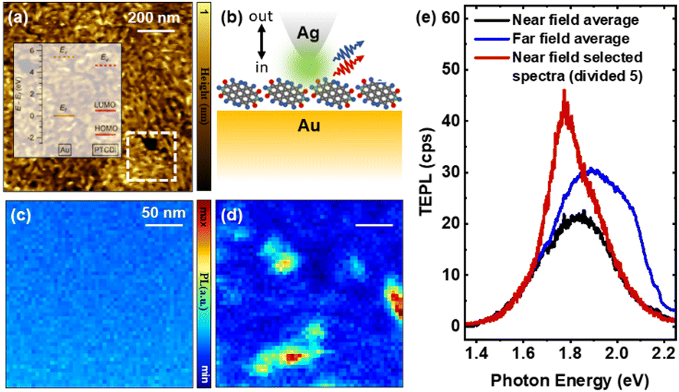 | ||
| Fig. 1 (a) Topographic AFM image of a PTCDI thin film on gold. The TEPL measurements track exciton transitions within the white dashed area. (b) Schematic representation of the nano-topical measurement that consists of tip-out (c) and tip-in (d) images recorded at every spatial position, where the tip is either 30–40 nm away from the surface (c) or in direct contact (d) with it. Note that tip-in and tip-out spectra are also termed far field and near field in (e), where selected spectra showing TEPL enhancement are simultaneously plotted. Conditions: 532 nm continuous wave laser source, 50 μW at the sample position, 0.5 s integration time at each pixel, 5 nm lateral/vertical steps in (c) and (d). | ||
Selected area topographic and nano-optical maps that expose the heterogeneity of the recorded optical response are shown in Fig. 2. Note that the area spanned by the topographic and nano-PL maps in Fig. 2b–d roughly correspond to a diffraction limited spot. In other words, conventional optical microscopy and spectroscopy measurements cannot resolve the observed heterogeneity within the analyzed area. Indeed, TEPL mapping allows us, e.g., to between nano-domains of PTDCI (see highlighted oval areas in Fig. 2b–d) at which photoluminescence is dominated by intermolecular excitons vs. vibronic sub-bands. This is perhaps most visible in the composite map that tracks both mechanisms. Beyond clear correlations between topographically distinct features (Fig. 2a) and TEPL maps (Fig. 2b–d), our measurements also reveal correlations between the measured heights and the nature of the excitonic transitions in the film. For instance, thicker regions seem to support intermolecular excitons, whereas thinner regions feature dim/quenched TEPL. These two observations can be readily understood. The higher availability of molecules in the thicker portions of the films increases the probability of interlayer exciton-driven PL, whereas charge transfer between PTCDI molecules and the underlying gold film led to quenched emission. Indeed, the interplay between enhanced absorption and quenched emission underlies TEPL. The latter would be expected to dominate in the thinner films. This can be further confirmed with a statically analysis of intensities for each height. These distributions can be found in the ESI† (Fig. S2) along a detailed explanation of the physical mechanisms involved.
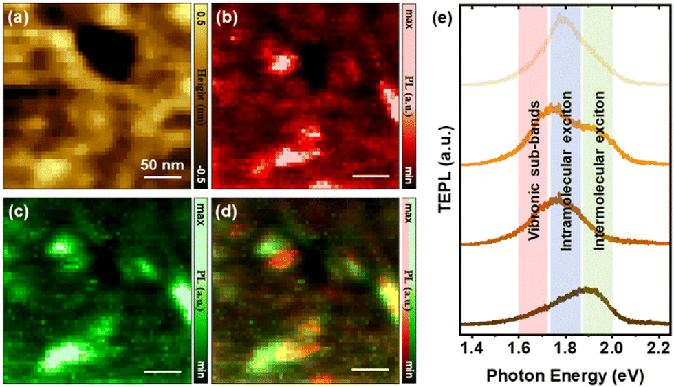 | ||
| Fig. 2 Topographic AFM map (a) and TEPL maps in the 1.60–1.72 (b) and 1.87–1.99 (c) eV regions are shown along with a composite TEPL map that tracks both intermolecular excitons and vibronic sub-band-mediated PL. The selected energy maps are chosen such that they track different contributions to PTCDI emission, as illustrated through the selected spectra plotted in (e). Conditions: 532 nm continuous wave laser source, 50 μW at the sample position, 0.5 s integration time at each pixel, 5 nm lateral/vertical steps in (c) and (d). | ||
To systematically examine the data and identify the dominant spectral modes in an unbiased fashion, we employ a variational autoencoder (VAE).26 VAE is an unsupervised deep learning technique based on the idea that complex experimental observations can be explained by a small number of latent variables. It is designed to learn the corresponding latent code, which is a probabilistic, compressed representation of input data, residing in a lower-dimensional space, from which the original data can be reconstructed. Implementation-wise, VAE learns how to compress the original observations into a small number of latent variables using an encoder neural network and then decompress the original observations back from that latent representation via another neural network called decoder. In the process, it learns the most important information needed to describe the whole dataset, while discarding all the information it considers irrelevant, such as measurement noise. The special regularization term in the VAE's training loss function ensures that the latent space is well-structured and continuous, making it interpretable and meaningful in the context of identifying dominant data modes. Recently, VAEs have been successfully applied to infer order parameters and detect phase transitions in theoretical lattice models27,28 and experimental datasets from electron and atomic force microscopies on 2D systems.29,30 The VAE was implemented using the pyroVED package (https://github.com/ziatdinovmax/pyroVED) with the default VAE training configuration.
The analysis of the latent manifold learned by the VAE (Fig. 3a) reveals that it successfully identified two dominant traits in the dataset. These are characterized by changes in peak intensity, represented by one latent variable, and shift in peak position, captured by another latent variable. Introducing additional latent variables did not contribute any further significant insights into the data's structure. Fig. 3b shows a one-dimensional cross-section of the learned latent manifold. This cross-section is taken along the axis of the second latent variable, holding the first latent variable (representing intensity) at a constant value. Note that we have the flexibility to generate any number of samples from the latent code and to select the grid density in the latent space at our discretion. This capability significantly enhances the visualization and interpretation aspects of our analysis. The analysis of the cross section reveals two modes at approximately 1.73 and 1.90 eV, which can be assigned to vibronic sub-bands and inter-molecular exciton, respectively. Additionally, another broader mode, characterized by a wider distribution of peak positions, is observed around 1.80 eV. This mode is likely associated with intramolecular excitons. This identification of peaks with the algorithm's output aligns closely with experimental results.20
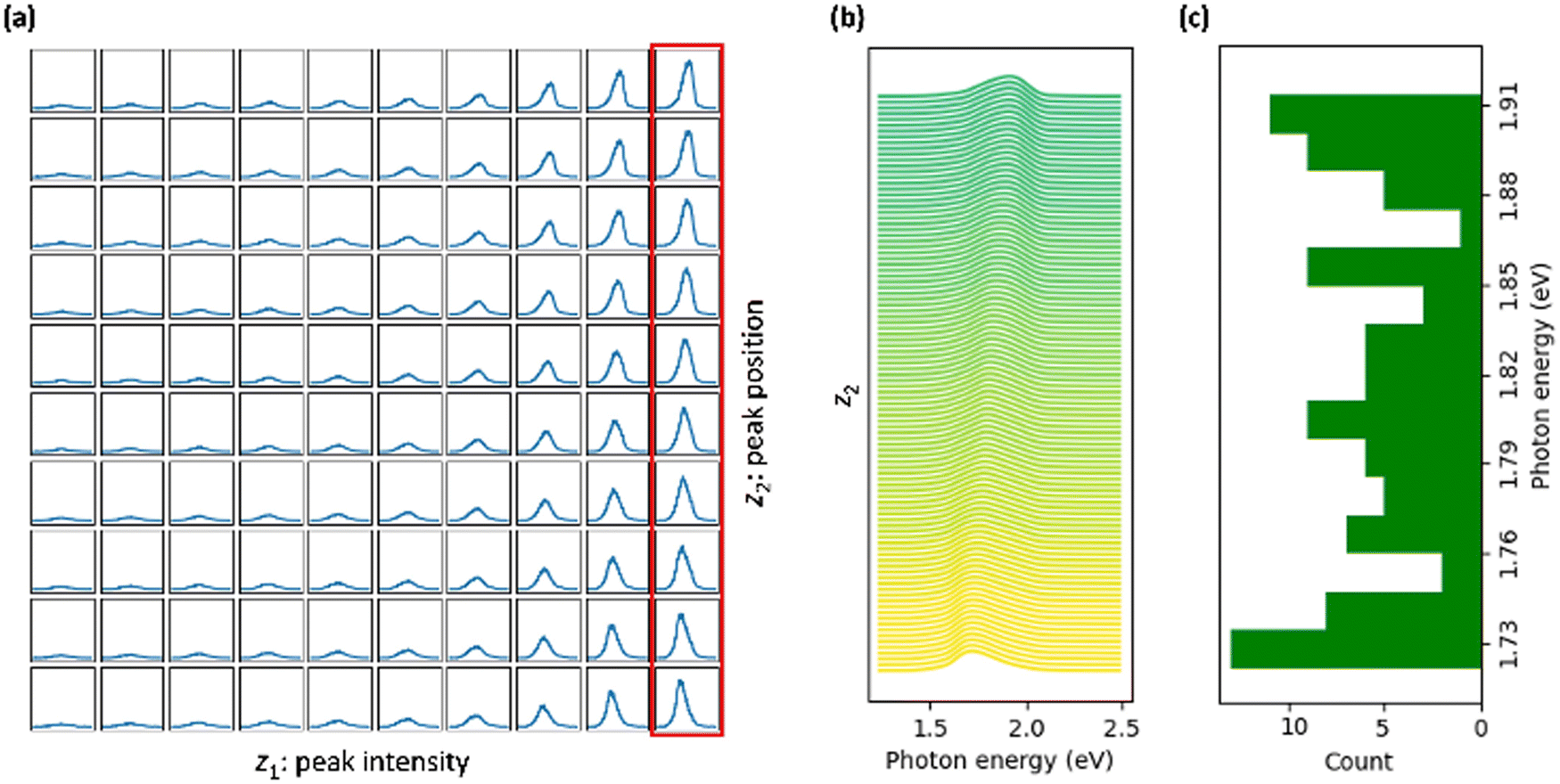 | ||
| Fig. 3 (a) The latent manifold learned by VAE where the first latent dimension (z1) corresponds to variation in peak intensity and the second latent dimension (z2) corresponds to variation in peak position. (b) Cross-section of the VAE latent manifold along the latent dimension associated with the peak position (red rectangular in (a)). The color gradient corresponds to a change in peak position and serves as a visual guide. (c) The histogram of the corresponding peak positions. | ||
The reproducibility of our observations and conclusions were ensured by repeating the above-described measurements over several regions of the film. Simultaneously recorded AFM-TEPL maps of a small region of the substrate are shown in Fig. 4. Here, we isolate an area that features localized PL emission to demonstrate our (measured) spatial resolution. It is important to distinguish between actual and measured spatial resolution. Whereas the first is governed by a combination of field localization and the so-called lightning rod effect,31 the latter is dictated by the spatial extend of the signal at the particular location imaged. Here, we show that a spatial resolution on the order of 10 nm is possible. This is not surprising given recent reports from our group in which sub-5 nm spatial resolution was demonstrated in both linear12 and nonlinear32 TEPL studies of excitonic materials. The contrast between the topographic resolution that is governed by a convolution between the tip and nanostructure shape and the TEPL resolution is immediately noticeable in Fig. 4c.
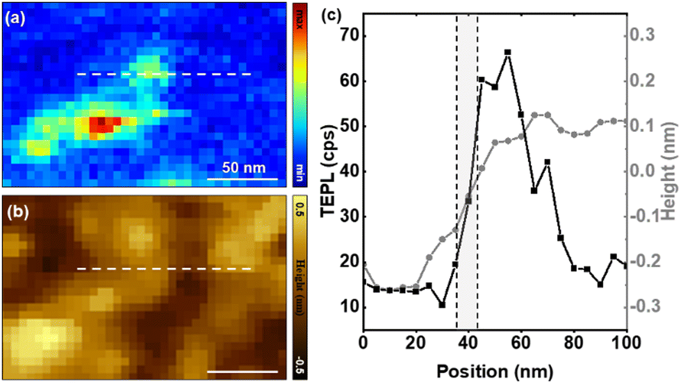 | ||
| Fig. 4 Simultaneously recorded selected area TEPL (at 1.87–1.99 eV) and AFM maps (b) are shown. TEPL and AFM cross-sectional cuts taken along the dashed lines in (a) and (b) are shown on the same plot in (c). Conditions: 532 nm continuous wave laser source, 50 μW at the sample position, 0.5 s integration time at each pixel, 5 nm lateral/vertical steps in (a). | ||
In summary, we show the power of TEPL in the context of mapping the optical and electronic properties of semiconductor thin films made of PTCDI. Enhanced scattering (up to 10×) and significantly improved spatial resolution (<10 nm, measured) over conventional PL allows us to track heterogenous spectral signatures on the nanoscale. The observed spectra that we were able to resolve individually can be associated with 3 different underlying mechanisms that depend on sample thickness and the nature of the underlying substrate. For instance, we observe dim PL in regions featuring thinner PTCDI coverage, which is unlikely to be the case for films supported on other (e.g., silicon) substrates. The generality of our observations therefore needs to be checked for different substrates. Notwithstanding the latter, the level of sensitivity and the high spatial resolution we demonstrate can be exploited in the quest to improve film quality or otherwise for quality control in the realm of optoelectronic device fabrication. Finally, we have demonstrated the utility of the unsupervised machine learning in identifying dominant traits in the hyperspectral dataset that have direct physical interpretation.
PVA, CFW, and PZE acknowledge support from the U.S. Department of Energy, Office of Science, Basic Energy Sciences, Chemical Sciences, Geosciences, and Biosciences Division, Condensed Phase and Interfacial Molecular Science program, FWP 16248. MZ acknowledges the Laboratory Directed Research and Development Program at Pacific Northwest National Laboratory, a multiprogram national laboratory operated by Battelle for the U.S. Department of Energy. KR and WLC acknowledge support from the U.S. Department of Energy, Office of Science, Office of Basic Energy Sciences, Chemical Sciences, Geosciences, and Biosciences Division under Award Number DE-SC0024525.
Conflicts of interest
There are no conflicts to declare.Notes and references
- J. H. Burroughes, C. A. Jones and R. H. Friend, Nature, 1988, 335, 137–141 CrossRef
.
- A. Facchetti, Mater. Today, 2007, 10, 28–37 CrossRef CAS
- K. Liu, B. Ouyang, X. Guo, Y. Guo and Y. Liu, npj Flexible Electron., 2022, 6, 1 CrossRef CAS
- G. Horowitz, D. Fichou, X. Peng, Z. Xu and F. Garnier, Solid State Commun., 1989, 72, 381–384 CrossRef CAS
- T. Kim, J.-H. Kim, T. E. Kang, C. Lee, H. Kang, M. Shin, C. Wang, B. Ma, U. Jeong, T.-S. Kim and B. J. Kim, Nat. Commun., 2015, 6, 8547 CrossRef CAS PubMed
- G. Gustafsson, Y. Cao, G. M. Treacy, F. Klavetter, N. Colaneri and A. J. Heeger, Nature, 1992, 357, 477–479 CrossRef CAS
- F. Cicoira, C. Santato, F. Dinelli, M. Murgia, M. A. Loi, F. Biscarini, R. Zamboni, P. Heremans and M. Muccini, Adv. Funct. Mater., 2005, 15, 375–380 CrossRef CAS
- S. B. Jo, H. H. Kim, H. Lee, B. Kang, S. Lee, M. Sim, M. Kim, W. H. Lee and K. Cho, ACS Nano, 2015, 9, 8206–8219 CrossRef CAS PubMed
- V. Vohra, K. Kawashima, T. Kakara, T. Koganezawa, I. Osaka, K. Takimiya and H. Murata, Nat. Photonics, 2015, 9, 403–408 CrossRef CAS
- R. M. Stöckle, Y. D. Suh, V. Deckert and R. Zenobi, Chem. Phys. Lett., 2000, 318, 131–136 CrossRef
- H. Lee, D. Y. Lee, M. G. Kang, Y. Koo, T. Kim and K.-D. Park, Nanophotonics, 2020, 9, 3089–3110 CrossRef CAS
- C.-F. Wang, M. Zamkov and P. Z. El-Khoury, J. Phys. Chem. C, 2021, 125, 12251–12255 CrossRef CAS
- S. Mahapatra, D. Liu, C. Siribaddana, K. Wang, L. Li and N. Jiang, Chem. Phys. Rev., 2023, 4, 021301 CrossRef CAS
- J. Jelken, M. O. Avilés and F. Lagugné-Labarthet, ACS Nano, 2022, 16, 12352–12363 CrossRef CAS PubMed
- Z. Li and D. Kurouski, Acc. Chem. Res., 2021, 54, 2477–2487 CrossRef CAS PubMed
- P. Z. El-Khoury, Acc. Chem. Res., 2021, 54, 4576–4583 CrossRef CAS PubMed
- N. Kumar, A. Zoladek-Lemanczyk, A. A. Y. Guilbert, W. Su, S. M. Tuladhar, T. Kirchartz, B. C. Schroeder, I. McCulloch, J. Nelson, D. Roy and F. A. Castro, Nanoscale, 2017, 9, 2723–2731 RSC
- D. Zhang, X. Wang, K. Braun, H.-J. Egelhaaf, M. Fleischer, L. Hennemann, H. Hintz, C. Stanciu, C. J. Brabec, D. P. Kern and A. J. Meixner, J. Raman Spectrosc., 2019, 40, 1371–1376 CrossRef
- D. M. Marin, J. Castaneda, M. Kaushal, G. Kaouk, D. S. Jones and M. G. Walter, Chem. Phys. Lett., 2016, 659, 137–141 CrossRef CAS
- S. Le Liepvre, P. Du, D. Kreher, F. Mathevet, A.-J. Attias, C. Fiorini-Debuisschert, L. Douillard and F. Charra, ACS Photonics, 2016, 3, 2291–2296 CrossRef CAS
- H. Zhao, Y. Zhao, Y. Song, M. Zhou, W. Lv, L. Tao, Y. Feng, B. Song, Y. Ma, J. Zhang, J. Xiao, Y. Wang, D.-H. Lien, M. Amani, H. Kim, X. Chen, Z. Wu, Z. Ni, P. Wang, Y. Shi, H. Ma, X. Zhang, J.-B. Xu, A. Troisi, A. Javey and X. Wang, Nat. Commun., 2019, 10, 5589 CrossRef CAS PubMed
- V. R. Gangilenka, L. V. Titova, L. M. Smith, H. P. Wagner, L. A. A. DeSilva, L. Gisslén and R. Scholz, Phys. Rev. B: Condens. Matter Mater. Phys., 2010, 81, 155208 CrossRef
- H. Yamagata, J. Norton, E. Hontz, Y. Olivier, D. Beljonne, J. L. Brédas, R. J. Silbey and F. C. Spano, J. Chem. Phys., 2011, 134, 204703 CrossRef CAS PubMed
- F. C. Spano, Acc. Chem. Res., 2010, 43, 429–439 CrossRef CAS PubMed
- M. C. R. Delgado, E.-G. Kim, D. A. D. S. Filho and J.-L. Bredas, J. Am. Chem. Soc., 2010, 132, 3375–3387 CrossRef PubMed
- L. G. Kaake, G. C. Welch, D. Moses, G. C. Bazan and A. J. Heeger, J. Phys. Chem. Lett., 2012, 3, 1253–1257 CrossRef CAS PubMed
- T. Wang, T. R. Kafle, B. Kattel, Q. Liu, J. Wu and W.-L. Chan, Sci. Rep., 2016, 6, 28895 CrossRef CAS PubMed
- D. P. Kingma and M. Welling, Foundations and Trends® in Machine Learning, 2019, 12, 307–392 CrossRef
- A. Baul, N. Walker, J. Moreno and K.-M. Tam, Phys. Rev. E, 2023, 107, 045301 CrossRef CAS PubMed
- S. J. Wetzel, Phys. Rev. E, 2017, 96, 022140 CrossRef PubMed
- S. V. Kalinin, O. Dyck, S. Jesse and M. Ziatdinov, Sci. Adv., 2021, 7, eabd5084 CrossRef CAS PubMed
- C.-F. Wang, A. B. C. Mantilla, Y. Gu and P. Z. El-Khoury, J. Phys. Chem. A, 2023, 127, 1081–1084 CrossRef CAS PubMed
Footnote |
| † Electronic supplementary information (ESI) available. See DOI: https://doi.org/10.1039/d4cc01808g |
| This journal is © The Royal Society of Chemistry 2024 |