
 Open Access Article
 This Open Access Article is licensed under a
 Creative Commons Attribution 3.0 Unported Licence
Integration of a recyclable silver substrate for in situ surface-enhanced Raman spectroscopy in digital microfluidics†
Sebastian
Fehse‡
,
Anish
Das‡
 * and
Detlev
Belder
*
* and
Detlev
Belder
*
Institute of Analytical Chemistry, Leipzig University, Linnéstr. 3, D-04103, Leipzig, Germany. E-mail: anish.das@uni-leipzig.de; belder@uni-leipzig.de
First published on 3rd July 2024
Abstract
We report a new chip-integrated recyclable SERS substrate, achieved by photochemical deposition of silver nanoparticles onto titanium dioxide (TiO2) thin film. Facilitated by the photocatalytic activity of titanium dioxide the SERS substrate can be recycled for multiple analysis. This enables quasi-real time detection of various compounds in an automated and reusable DMF-SERS platform.
In chemistry, the integration of automated chemical micro-laboratories with advanced analytical techniques have transformed the way research is conducted by enabling more efficient methods for chemical processing, optimization and analysis.1 A perfect candidate as the automated micro chemical processing unit of such a self-driving laboratory is digital microfluidics (DMF).2 Here chemical droplets can be manipulated automatically on a programmable path by electric potentials. This has facilitated the study of various (bio) chemical processes,3 with significant applications in life sciences4 and chemistry.5 DMF allows seamless actuation of microliter to nanoliter-sized discrete droplets on a hydrophobic 2D electrode array based on the principle of electro-wetting on dielectric (EWOD).6 A typical DMF system works well as an mere automated sample processing unit which allows to execute chemical reactions by droplet merging, mixing and spliting.7 In order to fully utilize DMF as an enabling technology in chemistry, the chemical composition of each droplet should be analysed by an information rich detection technique such as NMR,8 mass spectroscopy9 and surface-enhanced Raman spectroscopy (SERS).10,11 Coupling digital microfluidics with SERS is promising, enabling label-free12 and non-destructive detection of various low-concentrated analytes.13 To achieve higher enhancement effects in SERS, compared to conventional Raman spectroscopy, suspended colloidal silver14 /gold15 nanoparticles (NPs) are usually mixed with the analyte solution. However, in context of lab-on-a-chip technology these suspended NPs can be problematic as they tend to contaminate the chip surface or negatively interfere with further downstream processes.16 To overcome these issues, and also to improve quantitation, stationary SERS substrates17 can be used. However, the integration of a stationary SERS substrate into a microfluidic system poses a new challenge, namely the irreversible adsorption of analyte,18 resulting in a so-called memory effect.19 This prevents the repeated use of a SERS substrate and, in the case of a chip-integrated stationary SERS-target, would make the chip a single-use device for only one detection event.
We recently, reported an approach to seamlessly combine DMF with off-chip stationary SERS-target.11 Here the memory effect was dealt with by using multiple replaceable ex situ SERS active substrate, so a new substrate was available for each measurement. If the SERS target is located inside the chip, replacing the target is not possible without disassembling the device. Therefore, to realize the full potential of DMF-based SERS detection for a broader application, the integrated SERS active spot on DMF should be sensitive, reproducible, and, most importantly, recyclable.
To remove the analyte molecules adsorbed on SERS active surfaces various approaches have been applied, however not in context with digital microfluidics.20 In this regard, the photocatalytic degradation approach21,22 using semiconductor oxides like TiO2 is advantageous as it is non-toxic, stable, biocompatible, and SERS compatible. Combining TiO2 with silver nanoparticles (AgNP@TiO2) allows for both SERS-based detection and photocatalytic degradation of organic molecules.
Therefore, the questions addressed in this work are: (a) can SERS active substrates be integrated into a DMF chip, (b) is the SERS substrate capable of sensitive Raman detection and (c) can the integrated SERS active substrates be recycled and reused? This is the starting point for this contribution, where we report the first on-chip integration of digital microfluidics and recyclable AgNP@TiO2 SERS substrate for in situ Raman spectroscopic detection.
The idea and general concept of this approach is shown schematically in Fig. 1. To realize this approach, a primary challenge was to develop a suitable TiO2 thin film layer inside the DMF chip. For this, the TiO2 thin film must possess transparency, stability, and should not disrupt the EWOD process. Furthermore, while aiming for surface modification with silver nanoparticles, the TiO2 thin film should exhibit the capability to regenerate the AgNP surface through the photodegradation of the analyte molecules under UV irradiation. Therefore, we fabricated the DMF chip with a top plate modified with the AgNP@TiO2 layer and the bottom plate adhered to a pre-existing electrode design (GaudiLabs, Switzerland). We synthesized the film layer from TiO2 precursor by modifying a method reported by Zhang et al.21 The fabrication steps are described in detail in the (ESI† S2–S4). The resulting TiO2 film was transparent, uniform and had good adhesion to the indium tin oxide (ITO) glass substrate (as seen in ESI† S3). Now, to integrate an AgNP@TiO2 SERS substrate for in situ SERS detection on DMF, an immobilized silver nanoparticle must not obstruct relative droplet movement (facilitate droplet removal from the spot after detection) and provide significant SERS enhancement. Therefore, the AgNP spots were integrated into the surface of the TiO2 film photo-chemically from silver nitrate solution using UV irradiation (ESI† S4) rather than simply drop-casting AgNP on top of the TiO2 film. This was followed by assembling the DMF plates with an inter-plate gap of 240 μm (ESI† S5). The chemical reagents were loaded on the reservoir electrode for all experiments such that each dispensed droplet, was approximately 1.46 ± 0.15 μL (ESI† S6).
 | ||
| Fig. 1 The Schematic illustrates the general approach. (a) Schematic side view of the bottom and top DMF plate with the AgNP@TiO2 SERS substrate integrated on the DMF top plate. Droplet A is actuated and parked underneath the SERS substrate and the analyte molecules adsorbed on the silver nanoparticles are excited with a green laser for SERS-based detection. (b) Droplet A is automatically actuated away and a new cleaning solution (Droplet C) is actuated towards the AgNP@TiO2 SERS substrate. The recycling process of the SERS substrate is initiated by activating the UV LED, leading to the photo degradation of the adsorbed analyte on the SERS substrate. | ||
Fig. 2a shows the DMF platform with the integrated SERS substrate mounted on a specially modified stage on the Raman microscope. The magnified image in Fig. 2b illustrates the deposition of approximately 1 mm (diameter) of AgNP spot on the TiO2 film surface inside the DMF chip. The silver nanoparticles were triangular in shape with average size calculated to be 175 nm (s.d ± 85.9 nm) from the SEM image in Fig. 2c. The TiO2 layer was characterised using X-ray powder diffraction (ESI† S8), which showed that the crystalline fraction in the TiO2 layer is made up of 87% Brookite, 11% Anatase and 2% Rutile. Such mixture of anatase-brookite TiO2 phase has been previously reported to show good photocatalytic properties for degradation of analyte molecules.23
 | ||
| Fig. 2 (a) An exemplary view of the experimental setup showing the DMF device with the integrated SERS substrate mounted on the Raman microscope. (b) A magnified view of the chip electrodes with the AgNP@TiO2 SERS substrate (1 mm diameter) integrated on the DMF top plate. (c) SEM image acquired showing the surface morphology of AgNP@TiO2 substrate. (d) Relationship between SERS intensity as a function of photo reduction time. The peak of methylene blue at 1447 cm−1 was used for calculating the mean intensity (N = 3). | ||
We optimized the AgNP deposition by investigating the effect of photo-reduction time on the SERS activity of methylene blue (MB). For this purpose, a modular confocal Raman microscope with a laser wavelength of 532 nm, excitation power of 13 mW and 1.08 μm laser spot size was used for the SERS measurement (ESI† S7). As shown in Fig. 2d, the photo-reduction time significantly influenced the performance of the AgNP@TiO2 substrate in terms of SERS activity. The SERS intensity of MB molecule at 1447 cm−1 increased gradually with increasing photo-reduction time and was highest at 20 min. Beyond 20 min, the SERS intensity increase was irregular, probably due to uneven deposition of the AgNP and also it was hard to perform SERS detection from the DMF chip top due to the denser amount of AgNP deposited. Therefore, a 20 min photo-reduction time was optimum for a homogenous immobilization of the silver ions on the TiO2 film.
After the successful fabrication and characterization of the SERS active spot @TiO2 substrate, it was crucial to determine the effectiveness of the SERS substrate in regards to SERS signal reproducibility before introducing it to the DMF/EWOD process. For this purpose, 4 μL of 10 μM MB solution in DI water/methanol (8![[thin space (1/6-em)]](https://www.rsc.org/images/entities/char_2009.gif) :2 vol%) was pipetted on the SERS substrate and dried at room temperature for 5 min. In Fig. 3a, the measured SERS spectra of MB are compared with the Raman spectrum during different fabrication stages. The spectra show that the TiO2 and AgNP@TiO2 layer induced no significant Raman band or auto-fluorescence over the selected spectral range. This proves the suitability of the substrate for SERS measurement without significant background interference. The SERS spectrum obtained from MB molecules adsorbed on the surface of AgNP@TiO2 had distinct peaks at 448, 498, 596, 674, 774, 894, 956, 1043, 1160, 1310, 1400, 1447, and 1628 cm−1 respectively (ESI† S9). To assess the reliability of the fabricated chip integrated AgNP@TiO2 substrate, we examined the SERS signal reproducibility. Fig. 3b illustrates the reproducibility of the SERS signal showing the average column height for the SERS signal amongst five different substrates and its deviation. The relative standard deviation (RSD) is calculated to be within 9.51%, taking the major peak intensity of 1628 cm−1 as the evaluation standard (ESI† S17). This further verifies that the prepared SERS active surface is well suited for SERS detection. The limit of detection is 0.00696 μM for the given Raman parameters (ESI† S18).
:2 vol%) was pipetted on the SERS substrate and dried at room temperature for 5 min. In Fig. 3a, the measured SERS spectra of MB are compared with the Raman spectrum during different fabrication stages. The spectra show that the TiO2 and AgNP@TiO2 layer induced no significant Raman band or auto-fluorescence over the selected spectral range. This proves the suitability of the substrate for SERS measurement without significant background interference. The SERS spectrum obtained from MB molecules adsorbed on the surface of AgNP@TiO2 had distinct peaks at 448, 498, 596, 674, 774, 894, 956, 1043, 1160, 1310, 1400, 1447, and 1628 cm−1 respectively (ESI† S9). To assess the reliability of the fabricated chip integrated AgNP@TiO2 substrate, we examined the SERS signal reproducibility. Fig. 3b illustrates the reproducibility of the SERS signal showing the average column height for the SERS signal amongst five different substrates and its deviation. The relative standard deviation (RSD) is calculated to be within 9.51%, taking the major peak intensity of 1628 cm−1 as the evaluation standard (ESI† S17). This further verifies that the prepared SERS active surface is well suited for SERS detection. The limit of detection is 0.00696 μM for the given Raman parameters (ESI† S18).
 | ||
| Fig. 3 (a) Raman spectrum of different chip layers: ITO glass (cyan), TiO2 film (green), background spectrum of silver nanoparticles at TiO2 (red), and SERS spectrum of 10 μM methylene blue adsorbed on the surface of the complete SERS substrate (purple). (b) Substrate-to-substrate variation for five SERS substrates. The peak at 1628 cm−1 in the SERS spectrum was used to calculate the mean intensity (N = 5). | ||
After successfully developing and characterizing the SERS active spot @TiO2, it was used in a DMF workflow to assess the feasibility of using the SERS substrate multiple times for quasi- real-time monitoring of compounds and to investigate its recyclability properties. This is shown schematically in Fig. 4a–f (also ESI† S10, video S1). To achieve this, the DMF workflow was pre-programmed to automate the dispensing and actuation of MB droplets (10 μM) towards the SERS substrate using an electric potential of 280 Vp–p at 1.0 kHz (droplet speed: 2.75 mm s−1 (± 2.2%), ESI† S16, ESI† video 2). The Raman laser was activated and after SERS measurement, the analyte droplet is moved away using EWOD forces (step 4 in ESI† Video S1 and SS20). A cleaning solution (DI water/methanol (8:2 vol%)) was then applied and irradiated with a UV LED (340 nm, 60 mW) for 15 min, to initiate the recycling process, with the solution being exchanged every 5 min. After 15 min of UV irradiation the droplet shrinks but remains actuatable, allowing it to be moved, merged with a fresh droplet, and circulated to remove contaminants, as evident from the ESI† video 1. This process was repeated several times to achieve multiple recycling and detection cycles.
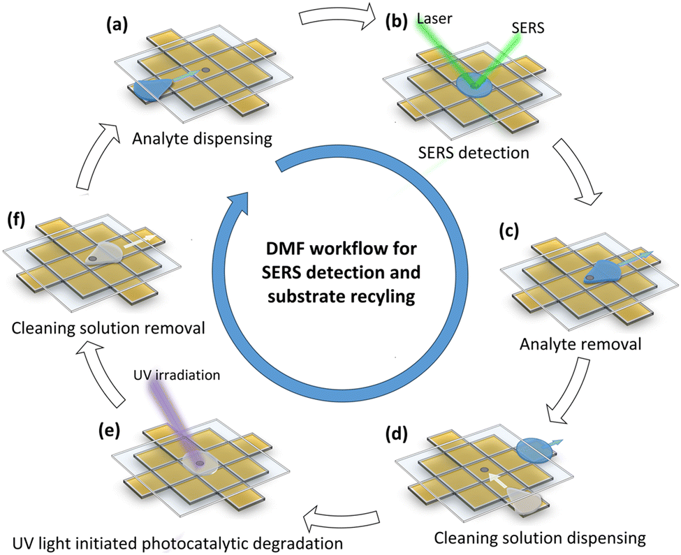 | ||
| Fig. 4 (a–f) Schematic for the droplet actuation steps inside DMF integrated AgNP@TiO2 SERS substrate for consecutive detection and recycling process. The blue arrow (inside chip) indicates the MB droplet actuation direction; the white arrow (inside chip) indicates the cleaning solution droplet actuation direction. | ||
The SERS substrates' performance was assessed by estimating the analytical enhancement factor (AEF) in the detection of MB (ESI† S11). The calculated AEF for the fabricated SERS substrate was 2.2 × 10⁵. Next, the on-chip recycling process of the AgNP@TiO2 SERS substrate was investigated. In Fig. 5a, an exemplary recorded SERS spectrum (at 0 min) is depicted, showcasing a methylene blue droplet during the automated DMF operation. The on-chip MB droplet has identical Raman bands as observed in the off-chip approach, thus affirming our DMF approach's suitability for sensitive chemical analysis. Fig. 5a shows the effect of the photocatalytic degradation time on the recorded SERS indicator band at 1628 cm−1 suggesting that the optimal time needed for efficient removal of the dyed analyte from the SERS substrate is 15 minutes. The insert image in Fig. 5a shows the extracted SERS spectra at different time intervals documenting the recycling progress. We also tested the system with a non-dyed analyte malathion (50 μM) as shown in Fig. 5b. The SERS spectra obtained at different UV irradiation time intervals on the DMF chip shows that SERS substrate for malathion can be recycled within 25 minutes. These spectra showcase the efficacy of the approach, with the SERS signal disappearing within a span of 15–25 minutes. The mechanism for this is explained in details in the ESI† 12. We also validated our DMF coupled-SERS substrate's regeneration capability in a set of on-chip control experiments with the same DMF actuation step but now only adding the cleaning solution without any UV (ESI† S13) and vice versa (ESI† S14).
 | ||
| Fig. 5 (a) SERS spectrum (0 min, purple) of the methylene blue droplet (10 μM, 1.46 μL) adsorbed on the SERS active surface after DMF actuation. Relationship between the SERS intensities at 1628 cm−1 peak from methylene blue versus the photocatalytic degradation time. The insert image illustrates the SERS spectra extracted from the SERS substrate for methylene blue at different time during the recycling process. (b) SERS spectra showing the photocatalytic degradation of malathion (50 μM, 2.5 μL) at different UV irradiation time interval. | ||
Fig. 6a shows five cycles for the detection and photocatalytic degradation process, where a strong SERS signal was observed from MB, while no distinct Raman peaks for MB were observed after UV irradiation, suggesting that the adsorbed analytes were decomposed to smaller inorganic molecules. Therefore, this substrate could be recycled and reused five times. This process was also repeated with malathion to demonstrate the robustness of the system (ESI† S19). Another essential criterion is the signal carryover effect. To investigate this, we analysed two different analytes, malachite green (MG) and methylene blue (MB), on the same DMF chip. The Raman peak can distinguish these two analytes at 1185, 1377 and 1600 cm−1, which appears only in the spectrum of MG but not for MB. These results shown in Fig. 6 demonstrate that the AgNP@TiO2 could successfully act as a recyclable SERS substrate without a carryover effect. With the same DMF-AgNP@TiO2 integrated chip, it was possible to perform consecutive detection & recycle with different analytes.
 | ||
| Fig. 6 (a) SERS spectra of MB (10 μM) adsorbed onto the DMF integrated AgNP@TiO2 SERS substrate showing five “detection-recycling” cycles. (b) SERS spectra of MB and MG (10 μM) on the SERS substrate in alternating detection processes before and after recycling. | ||
In summary, through the integration of SERS detection with a photochemical cleaning step within an automated DMF platform, a reusable DMF-SERS system was developed for the first time. Analyte molecules that would otherwise be irreversibly adsorbed on the SERS substrate underwent photocatalytic degradation upon exposure to ultraviolet irradiation and water droplets. Thereby, the memory effect of stationary SERS substrates inside the DMF chip was dealt with to a great extent. This approach broadens the analytical toolkit for in- situ SERS monitoring of compounds in quasi-real-time on a DMF platform unlocking the potential of DMF technology and its implications for future chemical research.
Financial support of the Deutsche Forschungsgemeinschaft (project numbers: 505692953/366065598) is gratefully acknowledged. We thank Dr S. Keilholz, M.Sc. L. Y. Dorsch and Prof. H. Kohlmann (Institute of Inorganic Chemistry, Leipzig University) for the measurement and interpretation of PXRD and also Dr D. Splith (Felix Bloch Institute for Solid State Physics, Leipzig University) for recording the SEM images.
Data availability
All the data supporting this article have been included as part of the and the ESI.†Conflicts of interest
There are no conflicts to declare.Notes and references
- M. Abolhasani and E. Kumacheva, Nat. Synth., 2023, 2, 483–492 CrossRef.
- M. J. Jebrail, et al., Lab Chip, 2012, 12, 2452–2463 RSC.
- H. Wang, et al., Front. Mech. Eng., 2017, 12, 510–525 CrossRef.
- F. Ahmadi, et al., Small, 2024, 20, 2308950 CrossRef CAS PubMed.
- S. Huang, et al., Sensors, 2020, 20, 1281 CrossRef CAS PubMed.
- A. Gupta, et al., ACM Trans. Des. Autom. Electron. Syst., 2019, 24, 21 CrossRef.
- D. Wang, et al., IEEE J. Electron Dev. Soc., 2023, 11, 411–415 Search PubMed.
- I. Swyer, et al., Lab Chip, 2016, 16, 4424–4435 RSC.
- A. Das, et al., J. Am. Chem. Soc., 2022, 144, 10353–10360 CrossRef CAS PubMed.
- Y. Wang, et al., Anal. Chem., 2018, 90, 5224–5231 CrossRef CAS PubMed; Z. Wang, et al., Sens. Actuators, B, 2024, 401, 134934 CrossRef.
- A. Das, et al., Anal. Chem., 2023, 95, 1262–1272 CrossRef CAS PubMed.
- R. Panneerselvam, et al., Lab Chip, 2022, 22, 665–682 RSC.
- J. F. Li, et al., Nature, 2010, 464, 392–395 CrossRef CAS PubMed.
- A. Pallaoro, et al., ACS Nano, 2015, 9, 4328–4336 CrossRef CAS PubMed.
- S. Abalde-Cela, et al., Sci. Rep., 2018, 8, 2440 CrossRef PubMed.
- S. Behzadi, et al., Chem. Soc. Rev., 2017, 46, 4218–4244 RSC.
- W. Yan, et al., Adv. Mater., 2017, 29, 1702893 CrossRef CAS PubMed; Y. Ou, et al., J. Phys. Chem. C, 2014, 118, 11478–11484 CrossRef.
- R. Panneerselvam, et al., Chem. Commun., 2018, 54, 10–25 RSC.
- D. Cialla, et al., Chem. Phys. Chem., 2008, 9, 758–762 CrossRef CAS PubMed.
- E.-M. Höhn, et al., Anal. Chem., 2019, 91, 9844–9851 CrossRef PubMed.
- Z. Zhang, et al., Appl. Surf. Sci., 2015, 359, 853–859 CrossRef CAS.
- Y. Zhao, et al., ACS Appl. Mater. Interfaces, 2014, 6, 5759–5767 CrossRef CAS PubMed; C.-H. Xiao, et al., RSC Adv., 2015, 5, 17945–17952 RSC.
- W. Nachit, et al., Opt. Mater., 2022, 129, 112256 CrossRef CAS; Z. Li, et al., ACS Catal., 2014, 4, 3273–3280 CrossRef.
Footnotes |
| † Electronic supplementary information (ESI) available. See DOI: https://doi.org/10.1039/d4cc01552e |
| ‡ These authors contributed equally. |
| This journal is © The Royal Society of Chemistry 2024 |