DOI:
10.1039/D3YA00231D
(Paper)
Energy Adv., 2023,
2, 1843-1858
Design and analysis of a SnS2/WS2/V2O5 double-heterojunction toward high-performance photovoltaics
Received
25th May 2023
, Accepted 8th September 2023
First published on 8th September 2023
Abstract
Tungsten disulfide (WS2) transition metal dichalcogenide (TMDC) absorber-based solar cells comprising tin disulfide (SnS2) buffer and vanadium (V) oxide V2O5 back surface field (BSF) layers have been designed and analyzed using a SCAPS-1D simulator in this study. The initial experimentation on back metal contact (BMC) and front metal contact (FMC) optimization involved the use of different materials to obtain the least resistive junction at the semiconductor–metal (M–S) interface, where the best potential was found. Following an extensive investigation nickel (Ni) and aluminum (Al) is determined to be the optimal material for the back and front contact, respectively. Subsequently, the impact of major parameters which affecting the photovoltaic (PV) performance, such as absorber layer thickness, doping concentration, bulk defect density, interface defect density, operating temperature, and surface recombination velocity, were studied systematically. An improved photoconversion efficiency (PCE) of over 32% (around 9% higher) was obtained with the open-circuit voltage (VOC) of 1.1 V, short-circuit current (JSC) of 37.2 mA cm−2, and fill factor (FF) of 84% with the Al/FTO/SnS2/WS2/V2O5/Ni heterostructure, compared to 23.4%, 0.89 V, 31.2 mA cm−2 and 81% for the pristine cell (without V2O5 BSF). These outcomes obtained from comprehensive studies reveal the huge potential of the SnS2/WS2/V2O5 double-heterostructure to be applied as a PV cell and pave a resourceful pathway for the experimental fabrication of WS2-TMDC absorber-based high-performance photonic devices.
1. Introduction
Energy demand is increasing quickly with the increase in population and rapid development of technology around the world; thereby, the predicted energy consumption is estimated to be 30 terawatts in 2050.1–3 Scientists and researchers are highly concerned with the reduction of existing fossil fuel resources, their annual rate of price increment, and their dangerous impact on global warming, leading to the depletion of the ozone layer and air pollution.4–8 Renewable energy derived from natural sources is abundant and sustainable, with the least impact on the environment. Solar energy, especially using photovoltaic technology, has the greatest potential, with the direct conversion of solar energy into electricity with a clean, economical, and sustainable pathway playing a key role in mitigating the global energy demand.9–12 Transition-metal dichalcogenides (TMDCs) used in thin-film solar cells are one of the most attractive absorber materials for use in photovoltaic devices.13–18 To date, there are several absorber semiconductors, including perovskites such as FeSi2, Sb2S3, Sb2Se3, MoS2, MoSe2, WS2, SnSx, Cu2MnSnS4, CsSnCl3, Cs2BiAgI6, CsPbBr3, Sr3NCl3, and Sr3AsI3, that show considerable potential to be used for fabricating high-performance solar cells.4–8 The choice of a favorable semiconductor as solar absorber material is a crucial issue to achieve the highest benefits, including inexpensive active materials, vacuum-free deposition, suitability for mass production, and markedly efficient power conversion.13,19–21 However, the challenges in fabricating highly efficient solar cells based on these materials include the use of rare-earth materials, scarcity, and material toxicity.19,20,22–24 Additionally, the development of heterostructured devices with band alignment fulfilling the criteria of an ideal required band structure to absorb the major portion of incident visible photons and thereby generation of electron–hole pairs, their dissociation, and collection efficiency at the external circuit, is still a challenge for high-performance photovoltaics beyond the Shockley–Queisser (SQ) limit.13,19–21
The WS2 layered material has emerged as a promising one to be used as an absorber material, with an optical absorption coefficient exceeding 105 cm−1, a tunable gap of 1.3–2.1 eV for bulk and monolayer film, and the high carrier mobility of 486 cm2 V−1 s−1 (at 5 K), while being much less hazardous and relatively abundant.25 Therefore, the choice of WS2 as a solar cell absorber may benefit the manufacture of inexpensive thin-film solar cells.26–31 The n-type electron transport layer (ETL), i.e., the buffer layer, has a vital impact on the cell's open-circuit voltage and short-circuit current density. The band alignment at the absorber/buffer interface i.e., band offset which is specially (CBO) determines the band bending at the interface is a spike that inhibits recombination. SnS2 is known as a low-cost, n-type layered semiconductor with nontoxic nature, having the tunable bandgap of 1.82–2.88 eV and electron mobility of 50 cm2 V−1 s−1.21 Several numerical and experimental studies report the use of WS2 as a solar cell photoactive material, with multiple heterostructures demonstrated.29–36 The PCE of 5.0% with 625 nm exposure and a power density of 2.5 mW cm−2 for the Au(10 nm)/WS2(20 nm)/Ag(200 nm) structure,37 and 0.31% with VOC of 0.551 V, JSC of 1.01 mA cm−2, and FF of 47.6% for the ITO/WS2 structure, have been obtained.32,33 However, the improved PCE of 17.73% for Al:ZnO/WSSe/WS2/TCO,30 25.71% in AZO/ZnO/WS2/Mo,35 28.86% for n-TiO2/p-WS2/p-Cu2O,38 and 29.74% for ZnO/CdS/WS2/Au34 heterostructures are predicted by developing double heterojunction structures. These theoretical outcomes reveal that the limited VOC obtained in WS2-based photovoltaics are observed mostly owing to the Fermi level pinning, which could be solved by adding an interlayer (back surface field [BSF] layer) between WS2 and the back metal contact, establishing a suitable band alignment with the least carrier recombination.31,39–41 Also, the smooth transfer of holes from the absorber to the back metallic contact is facilitated by the low valence band offset with a highly doped p-type BSF.42 Thus, the PCE could be enhanced effectively by reducing the valence band offset at the BSF/absorber interface, consequently developing a high activation energy that is almost equal to the absorber's band gap.43,44 Moreover, some inorganic metal oxides (MOs) such as vanadium pentoxide (V2O5), nickel oxide (NiO), and tungsten trioxide (WO3) have been incorporated as a BSF layer in numerous structures to enhance both cell performance and stability.45,46 Among them, p-type V2O5 (2.2 eV) showed promising features as BSF material, with moderate band gap, strong absorption coefficient, significant conductivity, and huge versatility, with abundance on Earth.11 With this perspective, the double junction heterostructure of SnS2/WS2/V2O5 with WS2 absorber, SnS2 buffer and V2O5 BSF layer shows a favorable band alignment required for spontaneous carrier transportation with insignificant offsets (CBO at the SnS2/WS2 interface of ∼0.19 eV and VBO at WS2/V2O5 of ∼0.26 eV), revealing its notable potential with nontoxic, low-cost and green characteristics for developing high-performance photovoltaics.
In this work, transition-metal dichalcogenide WS2-absorber-based high-performance thin film solar cells (TFSCs) with SnS2 and V2O5 as buffer and back surface field (BSF) layers, respectively, have been designed and analyzed using the SCAPS-1D simulator. Firstly, the influence of various possible metals as back contact was investigated to obtain the least resistive junction at the semiconductor–metal (M–S) interface. After that, the impacts of major affecting parameters such as absorber layer thickness, doping density, defect density, interface defect density, operating temperature, and its back surface recombination velocity with the buffer and BSF layers were investigated. A comprehensive simulation study reveals the huge potential of WS2, SnS2, and V2O5 as an absorber, buffer, and back surface field (BSF) layer, respectively, for the fabrication of high-performance economical and green thin film solar cells (TFSCs).
2. Device modeling and simulation parameters
The realization of high-efficiency solar cells can be obtained by numerical modeling and a systematic investigation of the role of each influential parameter of the designed cells. The one-dimensional electrical solar cell simulation software SCAPS-1D developed at the Department of Electronic and Information Systems at the University of Ghent in Belgium has shown potential to design and analyze TFSCs. Optoelectrical simulations of PV device structures consisting of up to seven semiconductor layers can be carried out using the SCAPS-1D software. The optoelectronic properties of PV cell structures can be predicted and analyzed by applying fundamental equations, as well as electrostatic potential and continuity equations, under steady-state conditions.47
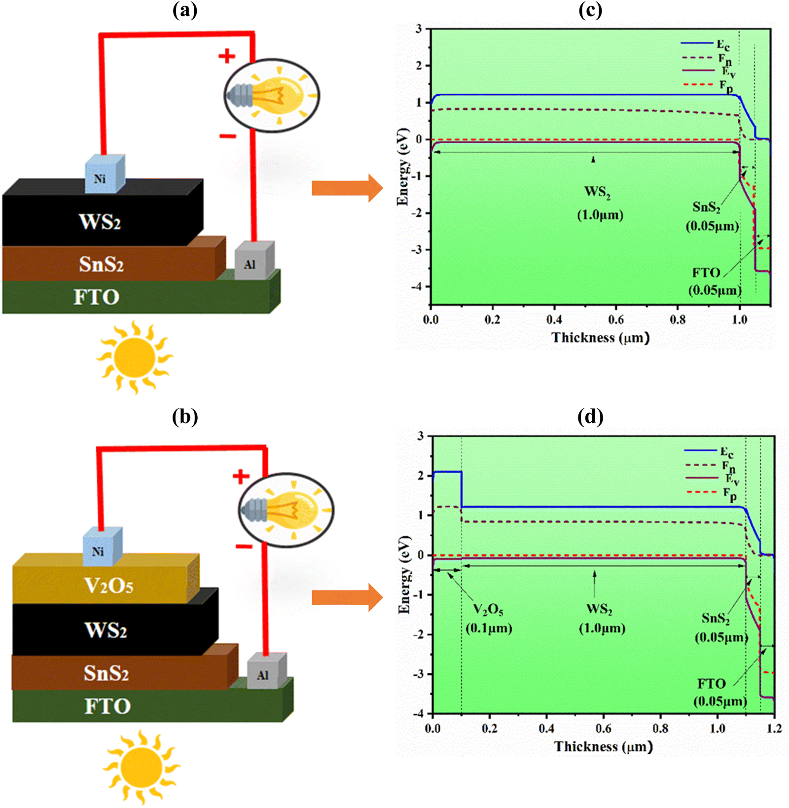
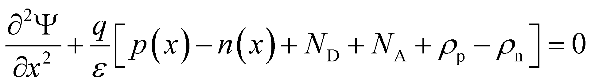
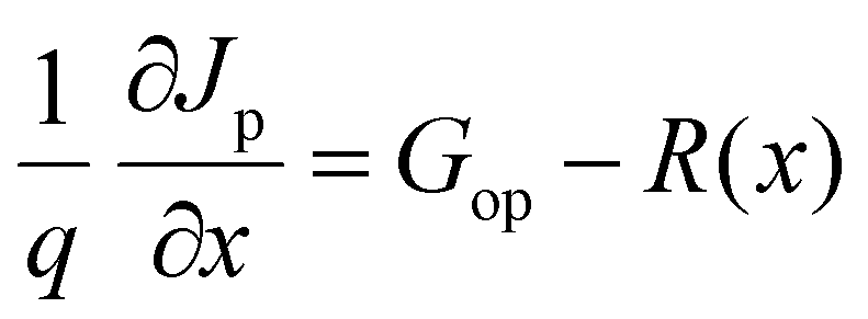
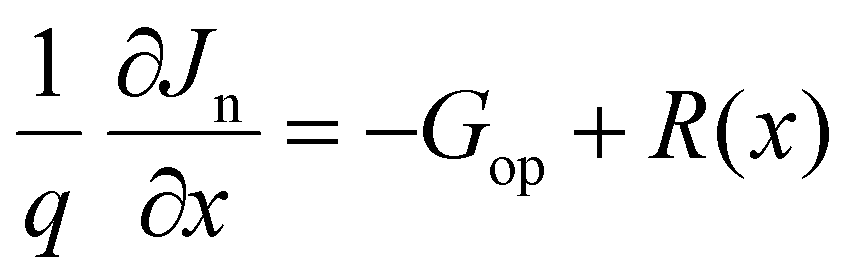
Fig. 1(a)–(d) shows the schematic diagram and corresponding energy band alignment with and without V2O5 BSF of the proposed thin-film solar architectures. In the adjusted heterostructure with V2O5 BSF of Al/FTO/SnS2/WS2/V2O5/Ni, p+–p–n–n+ junctions are formed with a p-type 1.0 μm WS2 absorber layer sandwiched between the highly doped p+-type 0.1 μm V2O5 BSF and n-type 0.05 μm SnS2 buffer layer. The FTO (0.05 μm) layer is used as a transparent conductive oxide (TCO) layer along with the back metal contact. In the energy band diagram simulation for the architecture of Al/FTO/SnS2/WS2/V2O5/Ni, the energy levels (both VB and CB) of the p-type V2O5 BSF layer and the n-type SnS2 buffer layer are notably higher than those of the WS2 absorber layer. The difference in the energy levels of the conduction band (CBO) between the BSF and the absorber is determined to be 0.91 eV, which facilitates the easiest path for transporting the photogenerated holes (PGHs), and conversely, it blocks photogenerated electrons (PGEs) passing into the back contact Ni (5.01 eV). The difference in the energy levels of the conduction band (CBO) between the buffer and the absorber is determined to be 0.95 eV. This energy difference accelerates the transport of photogenerated electrons (PGEs) and inversely repels the way of photogenerated holes (PGHs) into the front contact.
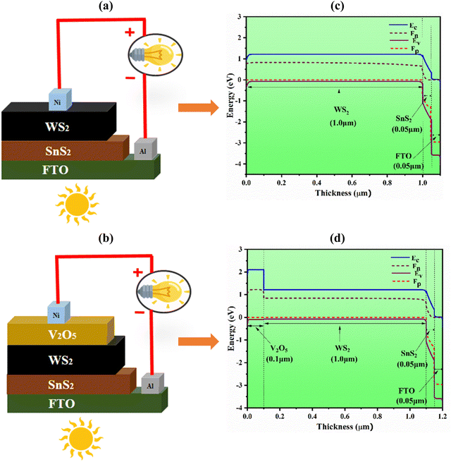 |
| | Fig. 1 (a) and (b) Schematic diagram and (c) and (d) corresponding energy band alignment with and without V2O5 BSF of the proposed heterostructures. | |
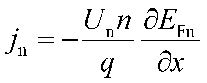
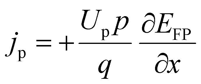
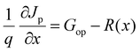
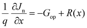
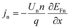
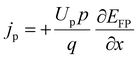
In the SCAPS-1D simulator, the fundamental equations of one-dimensional semiconductors, Poisson's equation, hole and electron continuity equations, as well as the drift and diffusion drift eqn (1)–(5)48–51 have been calculated to determine the PV parameters. The Poisson and continuity equations provide a set of coupled differential equations (Ψ, n, p) or (Ψ, EFn, EFp) with correct boundary conditions at interfaces and contacts. In this simulator, the intrinsic properties of each layer, such as layer thickness (nm); band gap Eg (eV); electron affinity χ (eV); dielectric permittivity εr; states density of the conduction band NC (cm−3); density of the valence band NV (cm−3); electron mobility μn (cm2 V−1 s−1); hole mobility μp (cm2 V−1 s−1); donor density ND (cm−3); acceptor density NA (cm−3); recombination coefficients (cm3 s−1) of radiative recombination, Shockley–Read–Hall recombination (SRH) and Augur recombination; and the absorption coefficient, are required to be provided from experimental outcomes as well as reported literature. The simulation was performed under AM 1.5G standard spectrum.
In this simulator, the absorption coefficient of each photoactive layer/material is required to be provided separately to simulate any homo/heterostructures from experimental results/literature, as summarized in Tables 1 and 2. The absorption coefficients of SnS2, WS2, and V2O5 were taken from reported literature.11,13,51–54 So, this modeling and the performed simulation is reliable. However, a noticeable discrepancy between simulation and experiment may be observed when the suggested device is fabricated experimentally owing to fabrication limitations, environmental impacts and measurement errors.
| |  | (1) |
| |  | (2) |
| |  | (3) |
| |  | (4) |
| |  | (5) |
where
ψ is the electrostatic potential;
ε0εr is the vacuum and semiconductor permittivity;
n and
p are free carrier concentrations; and
N+d and
NA are ionized donor and acceptor densities. The defect charge density is denoted by
ρdef;
G is the generation rate, and
jn and
jp are the electron–hole current densities;
q is the elementary charge;
Un and
Up are respectively electron and hole recombination rate;
μn and
μp are electron and hole mobility, respectively.
Table 1 Simulation parameters of the proposed (Al/FTO/SnS2/WS2/V2O5/Ni) solar cells
| Parameter (unit) |
n+-Type TCO (FTO)57 |
n-Type buffer (SnS2)52,53 |
p-Type absorber (WS2)13,54 |
p+-Type BSF (V2O5)11,51 |
| Thickness (μm) |
0.05 |
0.05 |
1.00 |
0.10 |
| Bandgap (eV) |
3.6 |
2.24 |
1.29 |
2.2 |
| Electron affinity (eV) |
4.50 |
4.24 |
4.05 |
3.40 |
| Dielectric permittivity (εr) |
10.0 |
10.0 |
13.6 |
8.00 |
| CB effective density of states (cm−3) |
2.0 × 10¹⁸ |
2.0 × 10¹⁸ |
2.2 × 10¹⁸ |
9.2 × 10¹⁹ |
| VB effective density of states (cm−3) |
1.8 × 10¹⁹ |
1.8 × 10¹⁹ |
1.8 × 10¹⁹ |
5 × 10²⁰ |
| Electron thermal velocity (cm s−1) |
2 × 10⁷ |
1 × 10⁷ |
1 × 10⁷ |
1 × 10⁷ |
| Hole thermal velocity (cm s−1) |
1 × 10⁷ |
1 × 10⁷ |
1 × 10⁷ |
1 × 10⁷ |
| Electron mobility (cm2 V−1 s−1) |
100 |
50 |
200 |
150 |
| Hole mobility (cm2 V−1 s−1) |
20 |
25 |
50 |
100 |
| Shallow uniform donor density ND (cm−3) |
1 × 10¹⁸ |
1 × 10¹⁷ |
— |
— |
| Shallow uniform acceptor density NA (cm−3) |
— |
— |
1 × 10¹⁸ |
1 × 10¹⁹ |
| Bulk defect density (cm−3) |
— |
1 × 10¹⁵ |
1 × 10¹⁴ |
1 × 10¹⁵ |
Table 2 Interface defect parameters of the proposed (Al/FTO/SnS2/WS2/V2O5/Ni) solar cells
| Parameters (unit) |
V2O5/WS2 |
WS2/SnS2 |
| Defect type |
Neutral |
Neutral |
| Capture cross-section of electrons (cm2) |
1 × 10⁻¹⁹ |
1 × 10⁻¹⁹ |
| Capture cross-section of holes (cm2) |
1 × 10⁻¹⁹ |
1 × 10⁻¹⁹ |
| Reference for defect energy level Et |
Above the highest Ev |
Above the highest Ev |
| Energy with respect to a reference (eV) |
0.6 |
0.6 |
| Total density (cm−2) |
1 × 10¹¹ |
1 × 10¹⁰ |
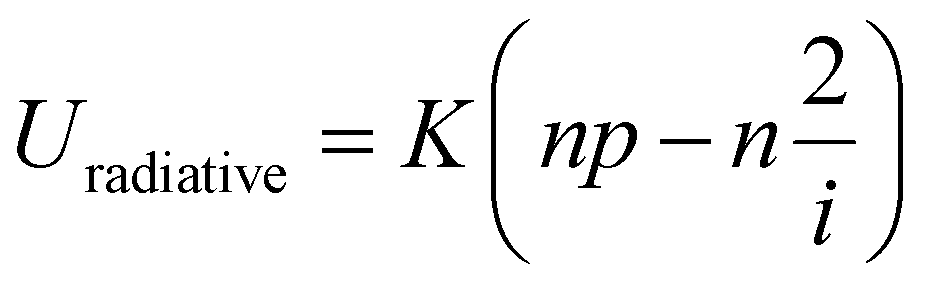
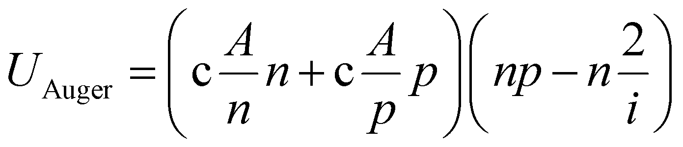
The radiative recombination, Shockley–Read–Hall recombination (SRH) and Augur recombination were considered with recombination coefficients of 2.0 × 10⁻⁹ (cm3 s−1), 1.0 × 10¹⁴ (cm3 s−1) and 1.0 × 10⁻²⁹ (cm3 s−1), respectively, in this study.
Recombination used for introducing the radiative and Auger (band-to-band) recombination in SCAPS-1D can be expressed as shown in eqn (6) and (7).55
| |  | (6) |
| |  | (7) |
Here,
cAn and
cAp can be set from literature;
i.e., for Si,
KSi = 1.8 × 10
−15 cm
−3 s
−1; GaAs,
KGaAs = 7.2 × 10
−10 cm
−3 s
−1; CIGS
K = 0; and the Auger constants are:
cAn ≈
cAp ≈ 3.0 × 10
−31 cm
−6 s
−1.
56
Table 1 lists the simulation parameters for the active layers used for modeling and designing the proposed devices. Herein, the thermal velocity of electrons and holes in each semiconductor at room temperature is fixed at approximately 107 cm s−1 throughout the study. The chosen value for surface recombination velocity of electrons and holes at the metallic contacts located at the front and back of the structure is 107 cm s−1. The chosen value for electron and hole capture cross-sections is 10−15 cm2. The work function referring to aluminum (Al) and nickel (Ni) was used as an optimized front and back metallic contact.13
3. Results and discussion
3.1 Influence of thickness and carrier concentration of WS2 absorber layer on PV performance
Fig. 2(a) displays how the performance parameters of the solar cell are influenced by changes in thickness within the range of 0.25–3.0 μm, keeping unchanged the rest of the parameters as shown in Tables 1 and 2, under AM 1.5G illumination at a constant working temperature of 300 K. The VOC is significantly changed at a thin absorber thickness of ≤1.0 μm. A markedly improved VOC (from ∼0.84 to ∼1.0 V) was seen in the solar cell structure with V2O5 BSF at the absorber thickness of 0.08–1.0 μm, which is consistent with previous reports.40,58 The efficiency of the cell increased from 16.03% to 27.06% and 25.88% to 32.09% for the heterostructure without and with BSF layer, respectively, with an increase in absorber thickness from 0.25–3.0 μm. The JSC increased almost linearly when absorber thickness was varied from 0.25–0.75 μm, and thereafter, it reached a saturated value of 35.6 (with BSF) and 33.7 mA cm−2 (without BSF) with further increase in absorber thickness beyond 0.75 μm. The enhancement in JSC values is a consequence of the increased absorption of incident photons at higher wavelengths in the WS2 absorber with the V2O5 BSF layer. Logically, an absorber with a higher thickness having BSF absorbs more photons, resulting in a greater number of electron–hole pairs (EHPs) generated.59,60 A smaller increase in FF was found at a lower thickness of <0.75 μm, which is almost constant over the absorber thickness of up to 3.0 μm. The tendency of reduction in VOC refers to the gradual increase of recombination of photogenerated carriers. This process may come to an end when the absorber thickness reaches >3.0 μm. The PCE gradually reduces (from 26 to 24%) at higher acceptor concentrations, above 1016 cm−3, when no BSF layer is added, while the PCE increases sublinearly after insertion of the V2O5 BSF between the WS2 absorber and Ni back contact.
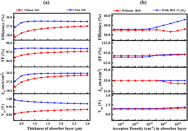 |
| | Fig. 2 Effect of absorber layer parameters: (a) thickness and (b) acceptor density with and without V2O5 BSF layer of the proposed heterostructure (Al/FTO/SnS2/WS2/Ni). | |
Though the performance parameters are insignificantly changed with an increase in acceptor concentration from 1010 to 1016 cm−3, surprisingly, a marked increase in PCE from 26.3% to 36.5% with FF from 77% to 81% and VOC from 0.77 V to 0.81 V was observed with increasing acceptor concentration from 1016 to 1020 cm−3 (Fig. 2(b)). This significant improvement was obtained due to the enhancement of carrier (hole) density, resulting in the formation of a strong built-in field, which causes the improved VOC as well as FF.
Fig. 3 shows the J–V characteristics and corresponding quantum efficiency (QE) response to varying absorber thicknesses from 0.25 to 3.0 μm for structures with and without the BSF layer, respectively. In Fig. 3(a), the photocurrent JSC increases exponentially from 27 to 36 mA cm−2 with an increase of absorber thickness in the entire region of 0.25 to 0.9 μm. The corresponding QE response demonstrates the improvement of photoabsorption by expanding the area coverage (indicated by arrow) with increasing absorber thickness, which causes the resulting enhancement in JSC (Fig. 3(b)). A similar characteristic was also observed in the structure without the BSF layer, having a current of 33 mA cm−2 and relatively smaller area of coverage in the QE response, as shown in Fig. 3(c) and (d). This is because a thicker absorber layer leads to an increase in cell resistance and diffusion length, which causes severe unwelcomed recombination of photogenerated carriers.59,61 Thereby, the optimal absorber thickness of 1.0 μm was used for further investigation based on the adjusted photovoltaic parameter values for both configurations, resulting in the highest η of 32.02% and 23.39% achieved for the structure with and without the BSF layer, respectively.
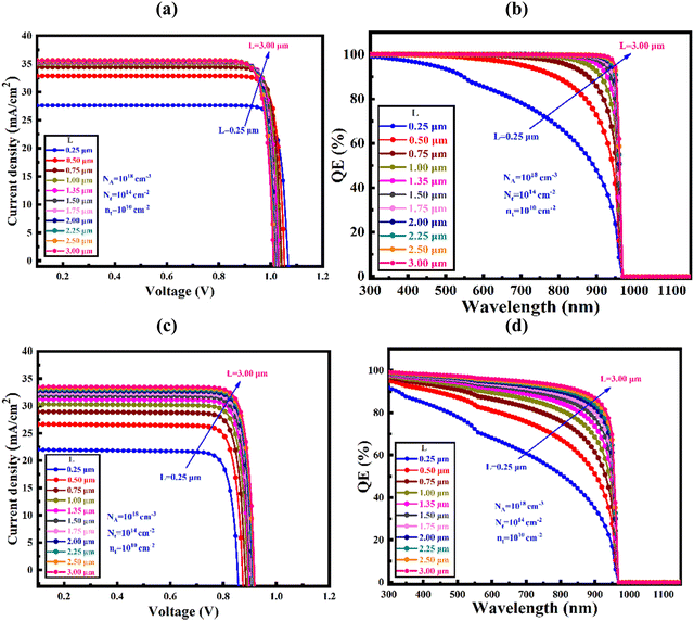 |
| | Fig. 3 Effects of absorber layer thickness on the J–V and Q–E of solar cells constructed (a) and (b) with BSF V2O5 and (c) and (d) without BSF V2O5, respectively. | |
There is a significant improvement in VOC with the increase in WS2 acceptor density from 1010 to 1020 cm−3. In the case with BSF, there is a shift in the VOC value from 0.918 to 1.152 V, whereas without BSF, the VOC value changes from 0.84 to 1.01 V, and the conversion efficiency increases from 25.82 to 36.07% due to the variation in acceptor density from 1010 to 1020 cm−3. Without the BSF layer, the JSC changes from 35.01 to 29.37 V, the FF from 84.73 to 88.22%, and consequently, the conversion efficiency changes from 24.83 to 26.08% with the acceptor density variation in the range of 1010–1020 cm−3. In both cases, FF and efficiency did not show appreciable changes with acceptor density up to 1015 at the WS2 absorber layer. To attain the best possible photovoltaic performance, this study has chosen the layer thickness of 1.0 μm and acceptor density of 1018 cm−3 in the WS2 absorber layer for further investigations.
3.2 Influence of thickness, carrier concentration, and defect density variation of SnS2 buffer layer on PV performance
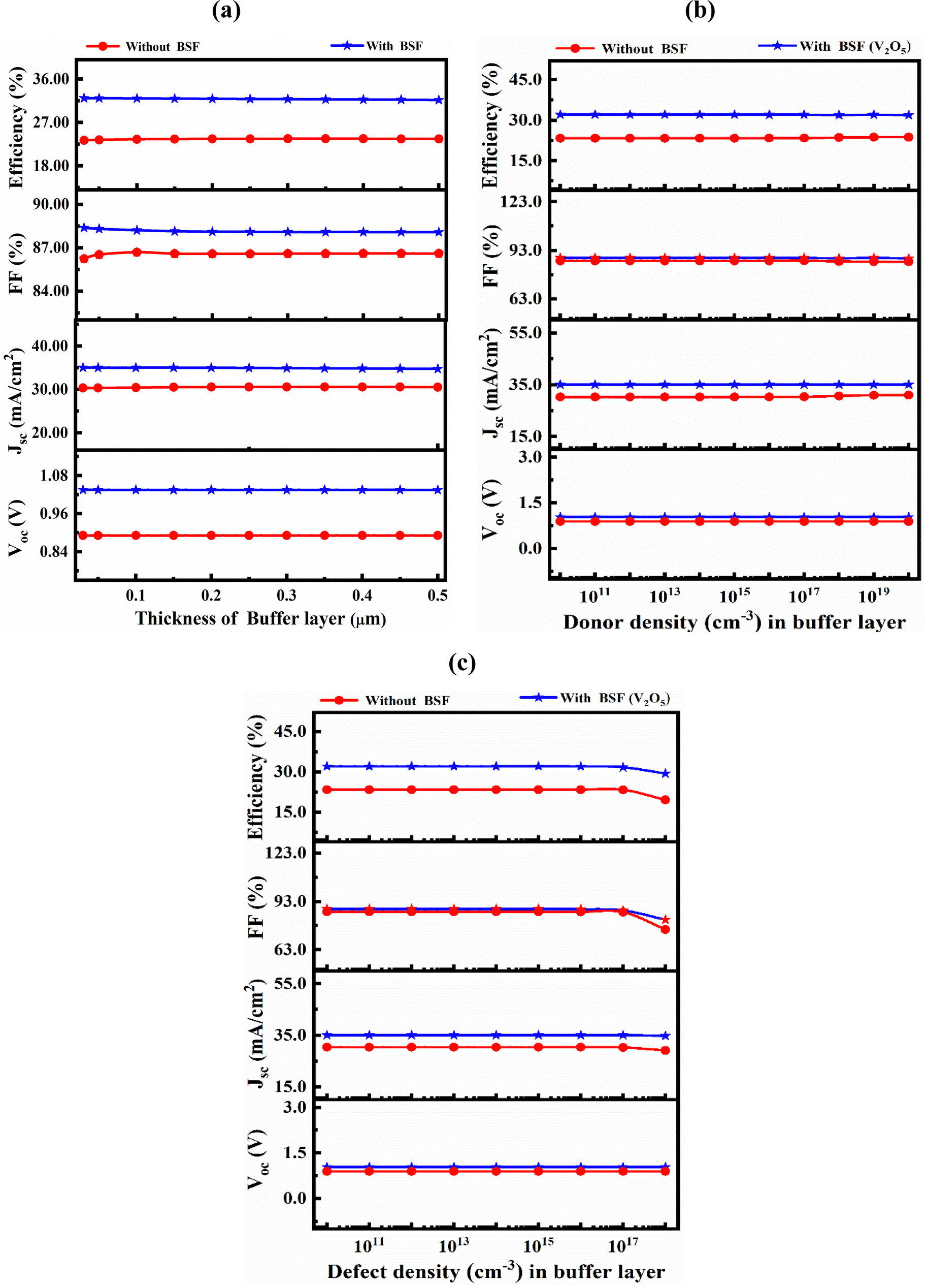
Fig. 4 illustrates the variation of photovoltaic parameters of the proposed thin film heterojunctions with varying layer thickness, carrier concentration, and defect density of the SnS2 buffer. In Fig. 4(a), PV parameters were found almost unchanged with the variation of SnS2 buffer layer thickness from 0.03 to 0.5 μm in both structures with and without the BSF. This may be due to the thin layer thickness with higher carrier density (∼1017 cm−3) of the SnS2 buffer layer. Considering an effective transmission of incident photons from SnS2 to WS2 absorber, a thin thickness of 0.05 μm was chosen as the optimal thickness of the SnS2 buffer layer. Further, an insignificant change in PV parameters was observed when the carrier concentration in SnS2 increased up to 1020 cm−3 in both structures, as depicted in Fig. 4(b). In the structure with BSF, the VOC, JSC, FF, and efficiency decreases from 1.035 to 1.030 V, 35.04 to 35.03 mA cm−2, 88.39 to 87.92%, and 32.05 to 31.72%, respectively, while these were changed from 0.891 to 0.890 V, 30.268 to 30.960 mA cm−2, 86.44 to 85.99%, and 23.32 to 23.74%, respectively, for the heterostructure without BSF.
 |
| | Fig. 4 Effect of varying (a) thickness, (b) donor concentration and (c) bulk defect density of the SnS2 buffer layer in both structures with and without BSF layer. | |
The photogenerated electrons would have to travel farther to get to the front contact as the SnS2 buffer layer's thickness increases, which would enhance the potential for carrier recombination. Therefore, the optimum values for thickness and doping concentration were found at 0.05 μm and 1017 cm−3, respectively, considering photon transmission and material utilization of the efficient buffer layer.
Fig. 4(c) shows the variation of PV parameters at different n-type defect densities of the SnS2 buffer layer from 1010 to 1018 cm−3, keeping unchanged the rest of the parameters. PV parameters drastically change as the bulk defect density increases from 1016 cm−3 for both scenarios with and without the BSF structure. An increase in bulk defect density in the SnS2 layer leads to an augmentation in the rate of Shockley-Read-Hall (SRH) recombination, causing a severe deterioration in the overall performance of cells.62 So, the optimum value of defect density should be lower than 1015 cm−3 to obtain the best performance from the proposed cells.62 Thus, a thickness of 0.05 μm, doping concentration of 1017 cm−3, with a defect density of 1015 cm−3 in SnS2, are optimal for use as a potential buffer in the proposed device structures.63
3.3 Influence of thickness and bulk defect density variation in the WS2 absorber layer on PV performance
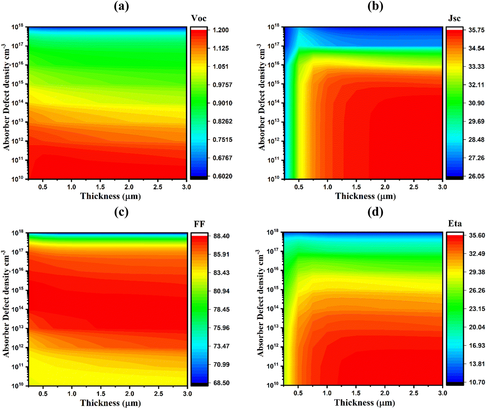
Fig. 5 illustrates the variation of PV parameters corresponding to relative bulk defect density and layer thickness of the WS2 absorber from 1010 to 1018 cm−3 and 0.25 to 3.0 μm, respectively. A marked reduction in solar cell parameters was found when the defect density of WS2 exceeds 1014 cm−3 with a layer thickness of ≥0.5 μm. The JSC, VOC, FF, and PCE of cells with BSF (Al/FTO/SnS2/WS2/V2O5/Ni) decreased from 35.71 to 26.05 mA cm−2, 1.2 to 0.6 V, 88.31 to 68.54%, and 35.55 to 10.78%, respectively, when the bulk defect density and absorber layer thickness were varied from 1010 to 1018 cm−3. In Fig. 5(a), the highest VOC of 1.0983 V is achieved when the BSF layer thickness is ∼1.0 μm and defect density is ≤1014 cm−3; however, it sharply dropped to 0.604 V at a defect density higher than this critical value (∼1014 cm−3). As shown in Fig. 5(b), the highest JSC value of 35.71 mA cm−2 was achieved at a defect density of ≤1016 cm−3 with layer thickness larger than 1.0 μm. The FF reached the maximum value of 88.31% when defect density was less than or equal to 1014 cm−3 and layer thickness was higher than 1.1 μm, so far, and it dropped noticeably to 68.54% corresponding to a defect density beyond 1014 cm−3, as shown in Fig. 5(c). As a result, the highest conversion efficiency, exceeding 30%, was obtained at a layer thickness of ∼1.0 μm and defect density of ∼1014 cm−3 (Fig. 5(d)). A high carrier recombination rate occurs across the cell as a result of the introduction of several defect states in the absorber layer, which in turn lowers cell performance.13,64,65 Thus, the highest PCE exceeding 32% with VOC of 1.035 V, a JSC of 35.03 mA cm−2, and an FF of 88.31% were obtained at a layer thickness and bulk defect density of ≥1.0 μm and ≤1014 cm−3 of the WS2 absorber, respectively.
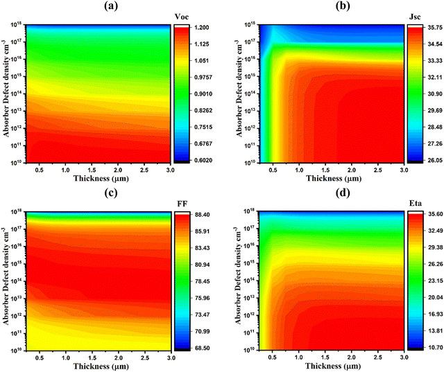 |
| | Fig. 5 Effects of WS2 absorber thickness and bulk defect density variations on the photovoltaic parameters: (a) VOC, (b) JSC, (c) FF, and (d) η. | |
3.4 Influence of layer thickness and interface defect density variation of the WS2 absorber on PV parameters
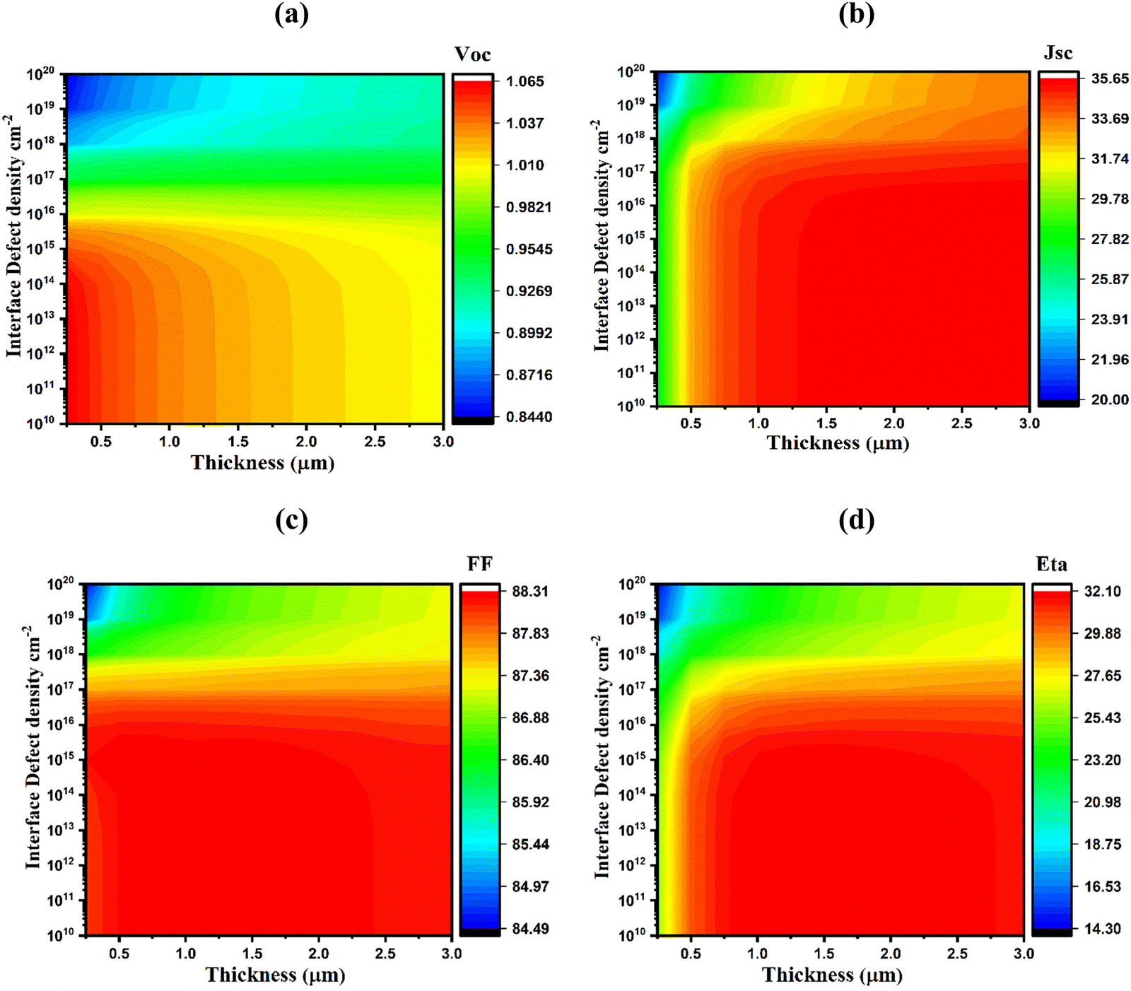
The quality of the interface has a significant impact on the cell's performance and thereby plays a vital role in the interaction between light and electricity. Fig. 6(a)–(d) displays the changes in PV parameters for various interface defect densities of 1010–1020 cm−2 for the V2O5/WS2 interface at a thickness of 0.25–3.0 μm of the WS2 absorber layer. The PV parameters were insignificantly affected at the interface defect density of ≤1010 cm−2, while they were markedly decreased with an increase in interface defect densities over 1014 cm−2 for both of the V2O5/WS2 interfaces. The JSC, VOC, FF, and PCE decreased from 35.64 to 20.04 mA cm−2, 1.065 to 0.845 V, 88.31% to 84.49%, and 32.1% to 14.3% for the structure with the BSF layer, while it drastically decreased from 35.641 to 1.971 mA cm−2, 1.065 to 0.455 V, 88.31% to 60.38%, and 32.09% to 0.65%, respectively, for the structure without BSF layer, which requires proper steps during practical cell fabrication to obtain the predicted optimized cell performance by tackling interface defects. Thus, the highest conversion efficiency of over 30% was achieved when the interface defect density was adjusted to ≤1016 cm−2 at a layer thickness of ∼1.0 μm of WS2 absorber.
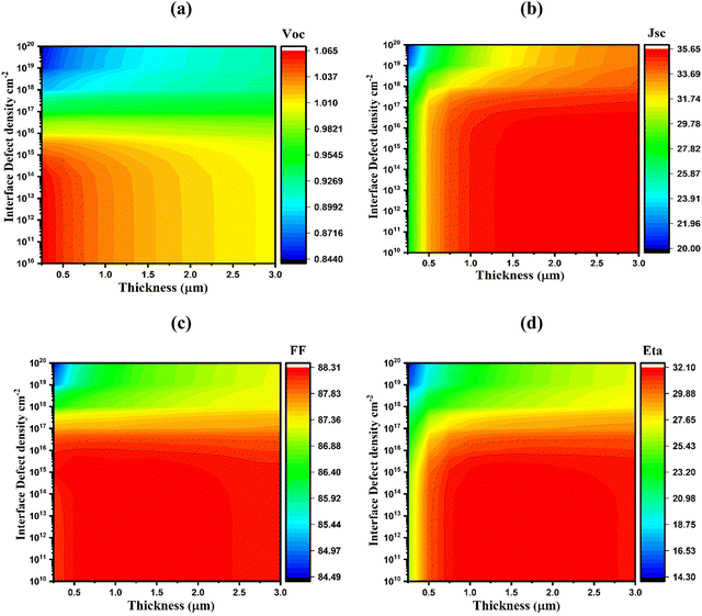 |
| | Fig. 6 Effects of absorber thickness and interface (V2O5/WS2) defect density variations on the photovoltaic parameters: (a) VOC, (b) JSC, (c) FF, and (d) η. | |
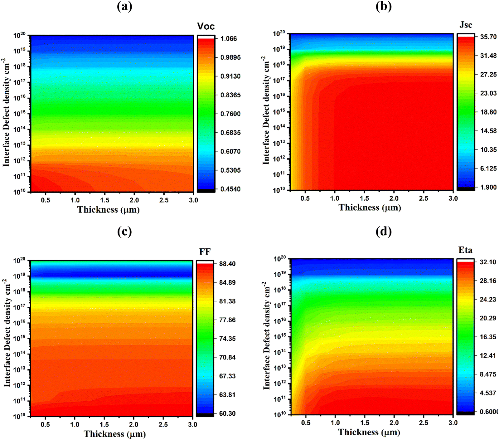
Fig. 7(a)–(d) depicts the change of PV with varying WS2/SnS2 interface defect density from 1010–1020 cm−2 and WS2 absorber layer thickness of 0.25–3.0 μm. The highest VOC of 1.098 V was obtained for all WS2 thicknesses when the defect density was below 1011 cm−2; however, it severely dropped from 1.098 to 0.464 V for the defect density beyond 1012 cm−2 (Fig. 7(a)). In Fig. 7(b), the maximum value for JSC of 35.642 mA cm−2 was achieved at a defect density of ≤1014 cm−2 and an absorber thickness of ≥0.75 μm. In the meantime, the FF decreased gradually from 88.31% to 72.41% at each thickness value of the WS2 absorber in the range of 0.25–3.0 μm and interface defect density of ≤1010 cm−2, as shown in Fig. 7(c). As a result, the highest conversion efficiency exceeding 30% was achieved at the defect density of ≤1011 cm−2 and absorber thickness of ≥0.75 μm, as demonstrated in Fig. 7(d). These detailed simulation outcomes reveal that the defects formed at the WS2/SnS2 interface have a severe impact on solar cell performance compared to defects at the WS2/WS2/V2O5 interface, which is consistent with reported studies.40,44
 |
| | Fig. 7 Effects of absorber thickness and interface (WS2/SnS2) defect density variations on the photovoltaic performance parameters: (a) VOC, (b) JSC, (c) FF, and (d) η. | |
3.5 Influence of the absorber layer's carrier concentration on the G–R profile
Fig. 8(a)–(d) demonstrates the impact on the carrier (electron and hole) concentration and total generation–recombination (G–R) profiles in configurations with and without the BSF layer at a constant acceptor concentration NA of 1018 cm−2 and defect density Nt of 1014 cm−2. Regardless of whether a solar cell has a back surface field (BSF) layer or not, the carrier concentration of the absorber layer shows a noticeable effect on G–R by the incident photon. In the cell structure of the BSF layer, a higher concentration of carriers in the WS2 absorber increased G–R recombination closer to the front surface of the cell. This happens due to an increase in available carriers at the higher carrier concentration, which leads to a rise in the rate of recombination. With a structure incorporating BSF, the impact of the carrier concentration in the absorber layer on the G–R profile is mitigated because of the formation of an aligned energy band with the least band offset among the absorber, BSF and metal contact. Because the BSF layer is designed to reduce recombination at the back surface of the cell, it can also affect the G–R profile near the front surface, which is consistent with previous reports.66 Total (electron and hole) generation at the absorber thickness of ∼1.0 μm was found to be the maximum, and on the contrary, resulted in the least total recombination loss.
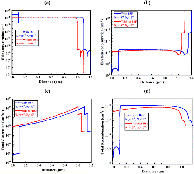 |
| | Fig. 8 Impact on (a) hole and (b) electron carrier concentration, (c) total generation, and (d) recombination of the absorber layer thicknesses. | |
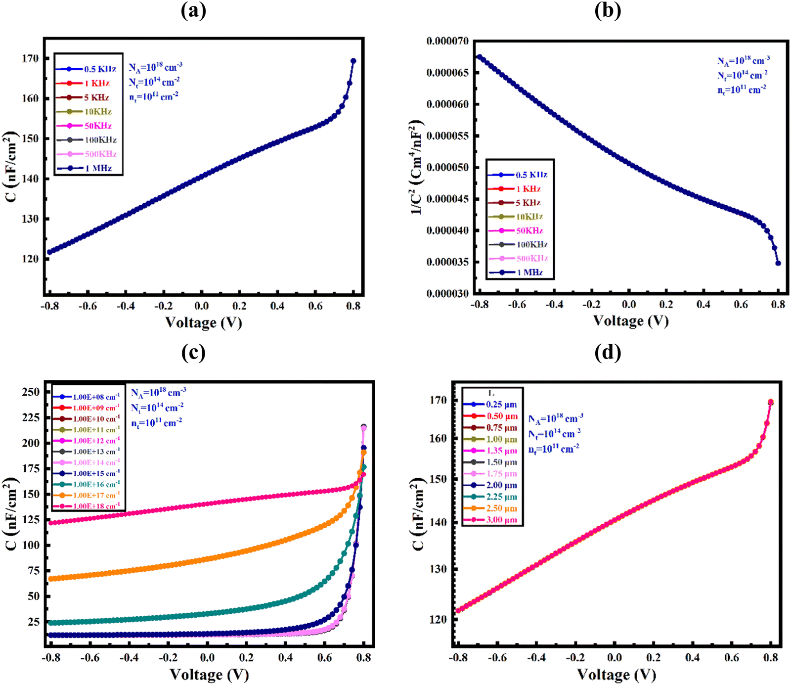
3.6 Capacitance–voltage (C–V) characteristics of the proposed heterojunctions
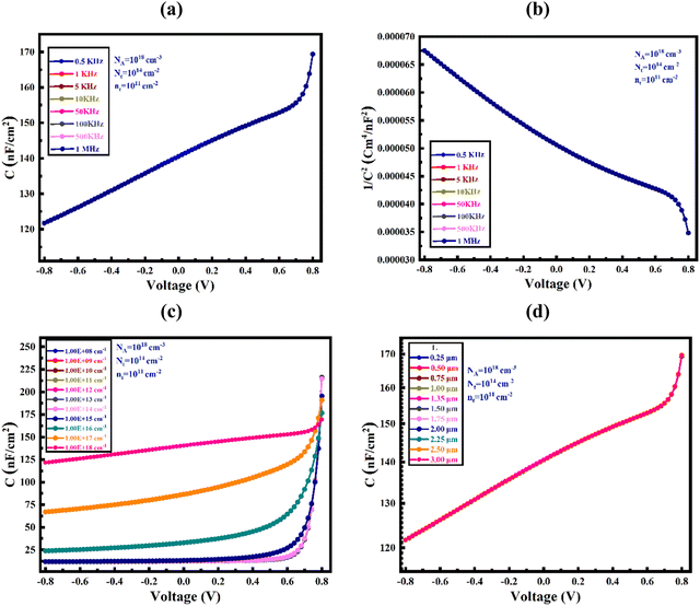
Fig. 9 illustrates the capacitance–voltage characteristics of the proposed heterojunction solar cells over a frequency range of 0.5 kHz to 1 MHz. Conventionally, p–n junctions are linked to the development of depletion and diffusion of charges. At reverse bias voltage, the depletion capacitance surpasses the diffusion capacitance, whereas the diffusion capacitance predominates at forward bias. These C–V characteristics under a range of frequencies, absorber concentrations, and thicknesses reveal the versatility of charge modulation in the proposed WS2-absorber-based solar cells. For a specific frequency, the capacitance increases sublinearly with the increase in polarization potential, which indicates a negligible acuity of the absorber traps at all frequencies, as shown in Fig. 9(a). Under reverse bias conditions, the existing traps are unable to mitigate the effective charge, leading to a decrease in capacitance, which is consistent with previous studies.67,68 With increasing carrier concentration, the capacitance increases markedly, while it is absolutely amplified with increasing polarization potential. Surprisingly, the capacitance increased almost linearly with absorber thickness up to 0.8 μm.
 |
| | Fig. 9 (a) Impact on C–V in solar cells with varying frequency; (b) 1/C2–V Mott–Schottky curve; C–V curves with (c) varying absorber doping and (d) varying absorber thickness. | |
Fig. 9(b) displays the Mott–Schottky plot of the proposed Al/FTO/SnS2/WS2/V2O5/Ni heterostructured cell. The intersection of the 1/C2 plot with the voltage axis gives rise to the flat-band potential of the proposed solar cell. The p-type WS2 layer is mostly occupied by the space charge area, as indicated by the negative slope of the plot, suggesting holes are the dominant carriers. The WS2 layer may have a high carrier density due to the photogenerated carriers caused by exposure to sunlight. A possible reason for the slight variation in 1/C2 is the presence of deep states in the absorber layer, which are localized. The deep states do not have a considerable effect; therefore, the modulation of majority carriers is the primary cause of the observed impact.67
Fig. 9(c) illustrates the capacitance–voltage (C–V) properties of a solar cell based on WS2 carrier concentration. The capacitance changes with increasing doping concentration of the absorber layer. As the forward bias voltage increases, the capacitance values increase and function sublinearly as Mott–Schottky junctions. The Mott–Schottky plot under AM 1.5G sunlight illumination indicated a lower built-in potential, which could be attributed to the capacitance generated by photogenerated carriers within photoactive materials. An earlier study reported that the increase in doping density leads to an increase in charge accumulation at the interface, which in turn results in an improvement in capacitance.69 In Fig. 9(d), the graph shows the relationship between capacitance and bias voltage at different absorber thicknesses at a constant frequency of 1 MHz. The change in capacitance with thickness variation shows an almost linear relation. However, after the voltage of 0.70 V, a significant rise in capacitance value is observed with the increase in voltage. Thus, the WS2 absorber has the potential to design high-efficiency photovoltaics with significant C–V behavior.
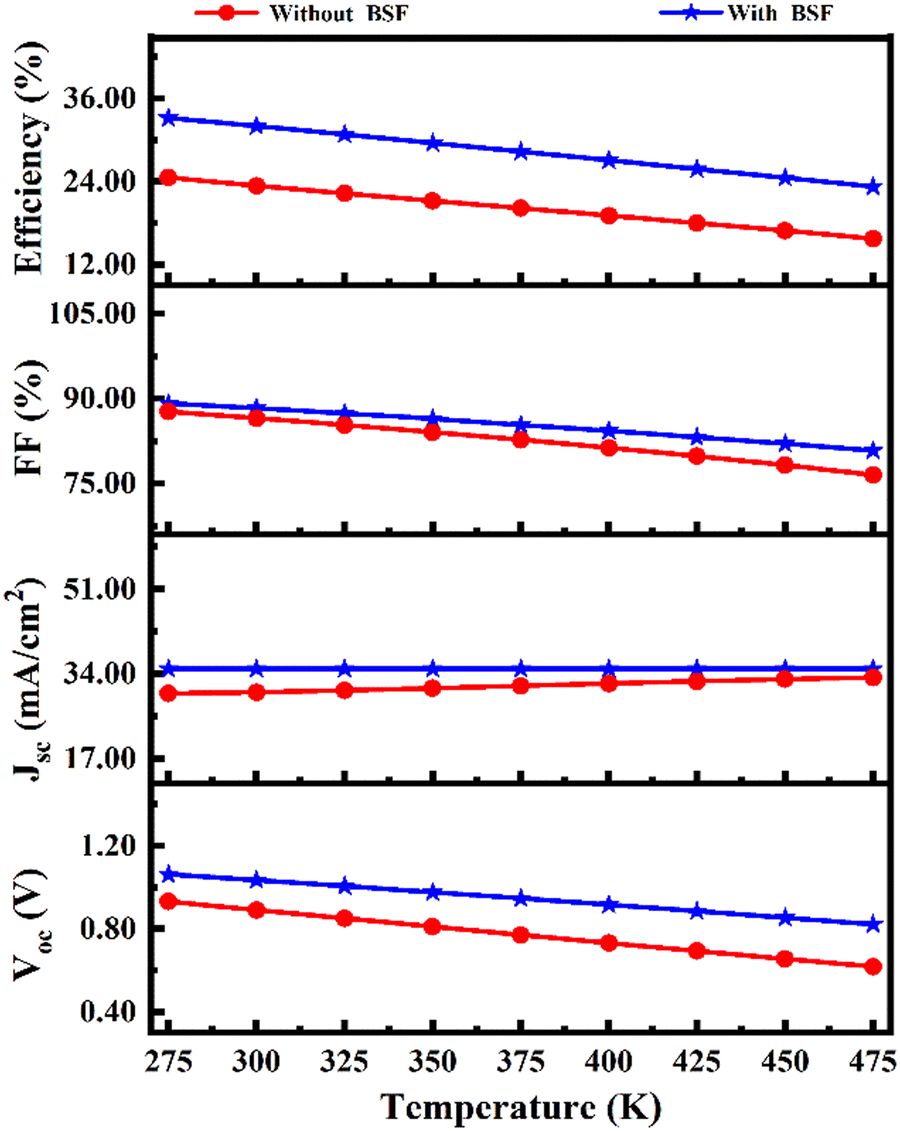
3.7 Influence of operating temperature on the performance of the solar cell
Fig. 10 illustrates the impact of operating temperatures on photovoltaic parameters of the proposed WS2-based solar cells for both configurations, with and without the BSF layer. The stability of the PV cell could be explored by the investigation of operating temperatures ranging from 275 to 475 K. A drastic reduction in PV parameters is observed for both WS2-based heterojunctions with and without V2O5 BSF when the working temperature rises from 275 to 475 K. The PCE decreased from 33.19% to 23.27% and from 24.56% to 15.75% as the operating temperature increased from 275 to 475 K for heterostructures with and without BSF, respectively. An increase in operating temperature leads to the shrinking of the band gap of WS2 and an increase in the reverse saturation current.70 As a result, the values of VOC, FF, and consequently the cell efficiency were affected noticeably at higher working temperatures. The declination in power conversion efficiency at higher operating temperatures observed in this study is consistent with previous reports.40,71–74
 |
| | Fig. 10 Effect of temperature on the PV parameters of the solar cell. | |
3.8 Performance of the device output
Fig. 11 displays the current density–voltage (J–V) characteristics of the WS2-based TFSCs. From Fig. 11, it is evident that the Al/FTO/SnS2/WS2/V2O5/Ni heterojunction solar cell exhibits a notably superior estimated current density compared to the reference WS2-based heterojunction solar cell, Al/FTO/SnS2/WS2/Ni. Without BSF, the WS2-based solar cell achieves a VOC of 0.89 V, JSC of 31.2 mA cm−2, FF of 81.0%, and power conversion efficiency of 23.4%. On the other hand, the configuration with BSF results in a VOC of 1.1 V, JSC of 37.2 mA cm−2, FF of 84.0%, and efficiency of 32.02%. The solar cell with BSF configuration achieves improved electrical device outputs in terms of VOC and JSC (as observed from the J–V analysis). This enhancement leads to an overall increase in the power conversion efficiency of the solar cell. Therefore, the inclusion of V2O5 as a BSF layer is suggested to significantly enhance the performance of the proposed WS2-based solar cell. In earlier experiments, CdS was used as buffer layer, which is toxic; here, SnS2 was used instead of CdS, being nontoxic and readily available.13,52Table 3 presents a comparative overview of the advantages brought about by the incorporation of V2O5 BSF in WS2 solar cells, along with its positive impacts when compared to analogous materials. The TFSCs proposed in this study could be more commercially attractive than other structures mentioned in Table 3.
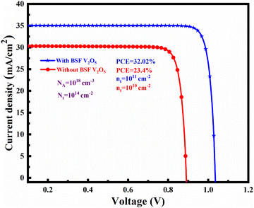 |
| | Fig. 11
J–V characteristics of the WS2-based solar cells. | |
Table 3 Summary of the reported experimental and theoretical work
| Sl No |
Type |
Cell structure |
Cell thickness (μm) |
V
OC (V) |
J
SC (mA cm−2) |
FF (%) |
η (%) |
Ref. |
| Note that * means this work, T = theoretical, and E = experimental. |
| 1 |
E |
ZnO/WS2 |
|
0.362 |
0.65 |
41.1 |
1.7 |
33
|
| 2 |
E |
ITO/WS2 |
|
0.551 |
1.01 |
47.6 |
3.9 |
33
|
| 3 |
E |
FTO/dye/WSG2 |
|
0.79 |
18.6 |
66 |
9.6 |
77
|
| 4 |
T |
ZnO/SnS2/CZTS/MoS2 |
0.08/0.05/1.5/0.1 |
0.7178 |
26.9976 |
65.67 |
12.73 |
52
|
| 5 |
T |
ZnO/ZnSe/WS2/Mg |
0.03/0.045/2.5/0.05 |
0.9 |
25 |
85 |
20 |
78
|
| 6 |
T |
ITO/WS2/CdS/Sb2Se3 |
0.025/0.05/0.06/0.4 |
0.706 |
40.52 |
72 |
20.6 |
79
|
| 7 |
T |
SnO2: F(FTO)/WS2/Cu2Te |
0.05/0.05/1.0 |
0.68 |
42.95 |
82.77 |
24.23 |
80
|
| 8 |
T |
ZnO: Al/ZnO/WS2 |
0.2/0.05/2 |
0.90 |
32.70 |
86.5 |
25.71 |
35
|
| 9 |
T |
Spiro-OMeTAD/CH3NH3PbI3/WS2 |
0.1/0.35/0.15 |
1.056 |
25.483 |
88.54 |
25.70 |
81
|
| 10 |
T |
FTO/n-WS2/Sb2S3 |
0.05/0.03/1.2 |
1.23 |
26.6 |
89.60 |
26.60 |
10
|
| 11 |
T |
FTO/n-WS2/Sb2Se3 |
0.05/0.03/1.2 |
0.85 |
38.40 |
86.56 |
28.20 |
10
|
| 12 |
T |
n-ZnO/n-CdS/p-WS2 |
0.2/0.05/2 |
0.8872 |
39.34 |
84.93 |
29.64 |
82
|
| 13 |
T |
FTO/CdS/WS2 |
0.05/0.05/1.0* |
0.83 |
31.88 |
83.66 |
22.09 |
13
|
| 14 |
T |
FTO/CdS/WS2/CuI |
0.05/0.05/1.0*/0.1 |
0.98 |
35.19 |
87.08 |
29.87 |
13
|
| 15 |
T |
FTO/SnS2/WS2 |
0.05/0.05/1.0 |
0.89 |
31.2 |
81 |
23.4 |
** |
| 16 |
T |
FTO/SnS2/WS2/V2O5 |
0.05/0.05/1.0/0.1 |
1.1 |
37.2 |
84 |
32.02 |
** |
In double heterostructures, with the insertion of a BSF layer like V2O5, the sub-bandgap photons may get absorbed significantly, specifically in the longer wavelength, which results in the improvement in photovoltaic performance. The sub-bandgap photons may be absorbed by the Urbach energy states, and these lower energy sub-bandgap photons participate in tail-state-assisted (TSA) two-step photon upconversion. These absorbed photons generate additional electron–hole pairs, resulting in a noticeable improvement in cell photocurrent. With the assistance of Urbach tail states, two sub-bandgap photons are absorbed in a row in this process. However, the degree of upconversion and the resulting enhancement in photocurrent depends on the Urbach energy, E0, of the photoactive material. This TSA upconversion takes place in a photoactive material when it possesses adequate doping concentration, high absorption coefficient and favorable bandgap.75,76 The higher Urbach energy significantly contributes to enhancing the quantum efficiency (QE), specifically in the longer wavelength.48–51,76 The equation for Urbach energy is shown in eqn (8). Thus, the authors believe that enhanced PV performance can be obtained in the proposed double-junction solar cells with relevant modelling and the convincing simulation parameter data.
| | α = α0![[thin space (1/6-em)]](https://www.rsc.org/images/entities/char_2009.gif) exp(E/Eu), exp(E/Eu), | (8) |
where
α is the absorption coefficient,
α0 is a constant,
E is the photon energy, and
Eu is the Urbach energy. The Urbach energy is calculated from inverse of ln
α vs. E slope.
4. Conclusions
Through numerical modeling with a SCAPS-1D simulator, high-efficiency transition metal dichalcogenide thin-film heterojunction solar cells with SnS2 buffer and V2O5 BSF layers have been explored. Potential V2O5 BSF and SnS2 buffer layer materials with the required layer properties, such as thickness, carrier doping concentration, and defect densities, have been investigated and adjusted through a comprehensive study. The best and adjusted layer thicknesses for the SnS2 buffer, WS2 absorber, and V2O5 BSF layer were found to be 0.05, 1.0, and 0.10 μm, respectively, with a bulk defect density of 1014 cm−3, and the interface defect densities of 1011 cm−2 at WS2/V2O5 and 1010 cm−2 at WS2/SnS2 were determined. These results indicate that the addition of a V2O5 BSF to the reference SnS2/WS2 TFSCs offers an efficient dual-heterojunction solar cell showing the improved (by almost 9%) PCE of 32.02% with VOC of 1.1 V, JSC of 37.2 mA cm−2 and FF of 84% for the Al/FTO/SnS2/WS2/V2O5/Ni heterostructure, compared to the PCE of 23.4% with VOC of 0.89V, JSC of 31.2 mA cm−2 and FF of 81% in the reference cell. The proposed WS2 cell has been shown to have better stability and performance than the reference WS2 solar cell. The results show the enormous potential of the SnS2/WS2/V2O5 heterostructure for designing and manufacturing high-efficiency photovoltaic cells and open a clear path for the production of WS2-based photovoltaic and photonic devices based on transition-metal dichalcogenides.
Author contributions
Md. Ferdous Rahman and Abdul Kuddus: conceptualization, methodology, software, validation, formal analysis, visualization, investigation, data curation, supervision, writing – original draft, review & editing. Jubair Al Mahmud: methodology, software, validation, formal analysis, visualization investigation, data curation, writing – original draft, review & editing. Md. Hasan Ali, A. T. M. Saiful Islam, Md Dulal Haque, Sheikh Rashel Al Ahmed, Muhammad Mushtaq, Abu Bakar Md. Ismail: validation, formal analysis, writing – original draft, review & editing.
Ethical approval
All authors declare that the manuscript does not have studies on human subjects, human data or tissue, or animals.
Conflicts of interest
The authors have no conflicts of interest.
Acknowledgements
The authors would like to offer their heartfelt appreciation to Dr Marc Burgelman and his colleagues at the EIS Department at the University of Gent in Belgium for providing the opportunity to use the SCAPS-1D software. The authors are also grateful to the Department of Electrical and Electronic Engineering, Begum Rokeya University, Rangpur 5400, Bangladesh, for the use of the Advanced Energy Materials and Solar Cell Research Laboratory.
References
- M. H. Ali, M. A. Al Mamun, M. D. Haque, M. F. Rahman, M. K. Hossain and A. Z. M. T. Islam, ACS Omega, 2023, 8, 7017–7029 CrossRef CAS PubMed.
- M. F. Rahman, J. Hossain, A. Kuddus, S. Tabassum, M. H. K. Rubel, M. M. Rahman, Y. Moriya, H. Shirai and A. B. M. Ismail, J. Mater. Sci., 2020, 55, 7715–7730 CrossRef CAS.
- A. Isha, A. Kowsar, A. Kuddus, M. K. Hossain, M. H. Ali, M. D. Haque and M. F. Rahman, Heliyon, 2023, 9, e15716 CrossRef CAS PubMed.
- A. Tolón-Becerra, X. Lastra-Bravo and F. Bienvenido-Bárcena, Renewable Energy, 2011, 36, 2067–2077 CrossRef.
- M. K. Hossain, A. A. Arnab, R. C. Das, K. M. Hossain, M. H. K. Rubel, M. F. Rahman, H. Bencherif, M. E. Emetere, M. K. A. Mohammed and R. Pandey, RSC Adv., 2022, 12, 34850–34873 RSC.
- M. K. Hossain, M. K. A. Mohammed, R. Pandey, A. A. Arnab, M. H. K. Rubel, K. M. Hossain, M. H. Ali, M. F. Rahman, H. Bencherif, J. Madan, M. R. Islam, D. P. Samajdar and S. Bhattarai, Energy Fuels, 2023, 37, 6078–6098 CrossRef CAS.
- M. K. Hossain, S. Bhattarai, A. A. Arnab, M. K. A. Mohammed, R. Pandey, H. Ali, F. Rahman, R. Islam, D. P. Samajdar, J. Madan, H. Bencherif, D. K. Dwivedi and M. Amami, RSC Adv., 2023, 13, 21044–21062 RSC.
- M. F. Rahman, N. Mahmud, I. Alam, M. H. Ali, M. M. A. Moon, A. Kuddus, G. F. I. Toki, M. H. K. Rubel, M. A. Al Asad and M. K. Hossain, AIP Adv., 2023, 13, 045309 CrossRef CAS.
-
M. Aghaei, Y. H. M. Thayoob, M. Imamzai, P. Piyous and N. Amin, 2013 IEEE 7th International Power Engineering and Optimization Conference (PEOCO), IEEE, 2013, pp. 203–208 Search PubMed.
- M. F. Rahman, M. M. Alam Moon, M. K. Hossain, M. H. Ali, M. D. Haque, A. Kuddus, J. Hossain and A. B. Abu, Heliyon, 2022, 8, e12034 CrossRef CAS PubMed.
- S. Ahmmed, A. Aktar, S. Tabassum, M. H. Rahman, M. F. Rahman and A. B. Abu, Superlattices Microstruct., 2021, 151, 106830 CrossRef CAS.
- M. F. Rahman, M. J. A. Habib, M. H. Ali, M. H. K. Rubel, M. R. Islam, A. B. Abu and M. K. Hossain, AIP Adv., 2022, 12, 1–11 CAS.
- M. M. Khatun, A. Sunny and S. R. Al Ahmed, Sol. Energy, 2021, 224, 956–965 CrossRef CAS.
- N. R. Paudel, K. A. Wieland and A. D. Compaan, Solar Energy Mater. Solar Cells, 2012, 105, 109–112 CrossRef CAS.
- M. Powalla, S. Paetel, E. Ahlswede, R. Wuerz, C. D. Wessendorf and T. Magorian Friedlmeier, Appl. Phys. Rev., 2018, 5, 041602 Search PubMed.
- C.-T. Lee, K.-F. Lu and C.-Y. Tseng, Sol. Energy, 2015, 114, 1–7 CrossRef CAS.
- A. Hu, J. Zhou, P. Zhong, X. Qin, M. Zhang, Y. Jiang, X. Wu and D. Yang, Sol. Energy, 2021, 214, 319–325 CrossRef CAS.
- M. Nakamura, K. Yamaguchi, Y. Kimoto, Y. Yasaki, T. Kato and H. Sugimoto, IEEE J. Photovolt., 2019, 9, 1863–1867 Search PubMed.
- C. Candelise, M. Winskel and R. Gross, Prog. Photovoltaics Res. Appl., 2012, 20, 816–831 CrossRef.
- L. A. Kosyachenko, X. Mathew, P. D. Paulson, V. Y. Lytvynenko and O. L. Maslyanchuk, Solar Energy Mater. Solar Cells, 2014, 130, 291–302 CrossRef CAS.
- N. Asim, K. Sopian, S. Ahmadi, K. Saeedfar, M. A. Alghoul, O. Saadatian and S. H. Zaidi, Renewable Sustainable Energy Rev., 2012, 16, 5834–5847 CrossRef CAS.
- D. J. Xue, B. Yang, Z. K. Yuan, G. Wang, X. Liu, Y. Zhou, L. Hu, D. Pan, S. Chen and J. Tang, Adv. Energy Mater., 2015, 5, 1–9 Search PubMed.
- T. M. Razykov, G. S. Boltaev, A. Bosio, B. Ergashev, K. M. Kouchkarov, N. K. Mamarasulov, A. A. Mavlonov, A. Romeo, N. Romeo, O. M. Tursunkulov and R. Yuldoshov, Sol. Energy, 2018, 159, 834–840 CrossRef CAS.
- E. S. Hossain, P. Chelvanathan, S. A. Shahahmadi, K. Sopian, B. Bais and N. Amin, Curr. Appl. Phys., 2018, 18, 79–89 CrossRef.
- M. W. Iqbal, M. Z. Iqbal, M. F. Khan, M. A. Shehzad, Y. Seo, J. H. Park, C. Hwang and J. Eom, Sci. Rep., 2015, 5, 1–9 Search PubMed.
- A. Matthäus, A. Ennaoui, S. Fiechter, S. Tiefenbacher, T. Kiesewetter, K. Diesner, I. Sieber, W. Jaegermann, T. Tsirlina and R. Tenne, J. Electrochem. Soc., 1997, 144, 1013–1019 CrossRef.
- S.-Y. Chen, C. Zheng, M. S. Fuhrer and J. Yan, Nano Lett., 2015, 15, 2526–2532 CrossRef CAS PubMed.
-
A. Jager-Waldau, M. C. Lux-Steiner, E. Bucher and G. Jager-Waldau, in Conference Record of the Twenty Third IEEE Photovoltaic Specialists Conference – 1993 (Cat. No. 93CH3283-9), IEEE, pp. 597–602.
- S. Roy and P. Bermel, Solar Energy Mater. Solar Cells, 2018, 174, 370–379 CrossRef CAS.
- R. Chaurasiya, G. K. Gupta and A. Dixit, Solar Energy Mater. Solar Cells, 2019, 201, 110076 CrossRef CAS.
-
K. Nassiri Nazif, A. Kumar, M. T. Moreira de Menezes and K. Saraswat, in Wide Bandgap Materials, Devices, and Applications IV, ed. M. Matin, A. K. Dutta and A. P. Lange, SPIE, 2019, p. 7 Search PubMed.
- C. Ballif, M. Regula, F. Lévy, F. Burmeister, C. Schäfle, T. Matthes, P. Leiderer, P. Niedermann, W. Gutmannsbauer and R. Bucher, J. Vac. Sci. Technol., A, 1998, 16, 1239–1243 CrossRef CAS.
- A. Jäger-Waldau, M. C. Lux-Steiner and E. Bucher, Solid State Phenom., 1994, 37–38, 479–484 Search PubMed.
-
A. K. Patel and B. P. Pandey, 2020 International Conference on Electrical
and Electronics Engineering (ICE3), IEEE, 2020, pp. 382–384 Search PubMed.
- K. Sobayel, K. S. Rahman, M. R. Karim, M. O. Aijaz, M. A. Dar, M. A. Shar, H. Misran and N. Amin, Chalcogenide Lett., 2018, 15, 307–315 CAS.
- K. Ellmer, Phys. Status Solidi B, 2008, 245, 1745–1760 CrossRef CAS.
- A. T. Nguyen, J. Wang, E. Cho, S. Lim, S. Kwon, J. Song, K. Zhou and D. W. Kim, Adv. Mater. Interfaces, 2023, 2300031, 1–7 Search PubMed.
- A. K. Singh, R. Walia, M. S. Chauhan, R. S. Singh and V. K. Singh, Environ. Sci. Pollut. Res., 2022 DOI:10.1007/s11356-022-24236-6.
- A. Ahmed, K. Riaz, H. Mehmood, T. Tauqeer and Z. Ahmad, Opt. Mater., 2020, 105, 109897 CrossRef CAS.
- S. R. Al Ahmed, A. Sunny and S. Rahman, Solar Energy Mater. Solar Cells, 2021, 221, 110919 CrossRef.
- M. K. Hossain, G. F. I. Toki, A. Kuddus, M. K. A. Mohammed, R. Pandey, J. Madan, S. Bhattarai, F. Rahman, D. K. Dwivedi, M. Amami, H. Bencherif and D. P. Samajdar, Mater. Chem. Phys., 2023, 308, 128281 CrossRef CAS.
- S. Z. Haider, H. Anwar, Y. Jamil and M. Shahid, J. Phys. Chem. Solids, 2020, 136, 109147 CrossRef CAS.
- T. Minemoto and M. Murata, Solar Energy Mater. Solar Cells, 2015, 133, 8–14 CrossRef CAS.
- Y. Cao, X. Zhu, H. Chen, X. Zhang, J. Zhouc, Z. Hu and J. Pang, Solar Energy Mater. Solar Cells, 2019, 200, 109945 CrossRef CAS.
- A. Kuddus, M. F. Rahman, J. Hossain and A. B. M. Ismail, EPJ Appl. Phys., 2020, 92, 1–14 Search PubMed.
- L. Zhang, C. Jiang, C. Wu, H. Ju, G. Jiang, W. Liu, C. Zhu and T. Chen, ACS Appl. Mater. Interfaces, 2018, 10, 27098–27105 CrossRef CAS PubMed.
- M. Burgelman, P. Nollet and S. Degrave, Thin Solid Films, 2000, 361–362, 527–532 CrossRef CAS.
- M. S. Chowdhury, S. A. Shahahmadi, P. Chelvanathan, S. K. Tiong, N. Amin, K. Techato, N. Nuthammachot, T. Chowdhury and M. Suklueng, Results Phys., 2020, 16, 102839 CrossRef.
- A. Ait Abdelkadir, E. Oublal, M. Sahal and A. Gibaud, Results Opt., 2022, 8, 100257 CrossRef.
- S. Ahmmed, A. Aktar, M. F. Rahman, J. Hossain and A. B. M. Ismail, Optik, 2020, 223, 165625 CrossRef CAS.
- A. Kuddus, M. F. Rahman, S. Ahmmed, J. Hossain and A. B. M. Ismail, Superlattices Microstruct., 2019, 132, 106168 CrossRef CAS.
- F. Belarbi, W. Rahal, D. Rached, S. Benghabrit and M. Adnane, Optik, 2020, 216, 164743 CrossRef CAS.
- M. Haghighi, M. Minbashi, N. Taghavinia, D. H. Kim, S. M. Mahdavi and A. A. Kordbacheh, Sol. Energy, 2018, 167, 165–171 CrossRef CAS.
- S. Roy and P. Bermel, Solar Energy Mater. Solar Cells, 2018, 174, 370–379 CrossRef CAS.
-
A. Niemegeers, M. Burgelman and K. Decock, SCAPS Manual Search PubMed.
- A. I. Likhter, E. G. Pel and S. I. Prysyazhnyuk, Phys. Status Solidi A, 1972, 14, 265–270 CrossRef CAS.
- M. F. Rahman, M. J. A. Habib, M. H. Ali, M. H. K. Rubel, M. R. Islam, A. B. M. Ismail and M. K. Hossain, AIP Adv., 2022, 12, 105317 CrossRef CAS.
- M. A. Matin, M. U. Tomal, A. M. Robin and N. Amin, Int. J. Photoenergy, 2013, 2013, 652695 CrossRef.
- M. M. A. Moon, M. F. Rahman, M. Kamruzzaman, J. Hossain and A. B. M. Ismail, Energy Rep., 2021, 7, 1742–1756 CrossRef.
- M. K. Hossain, M. H. K. Rubel, G. F. I. Toki, I. Alam, M. F. Rahman and H. Bencherif, ACS Omega, 2022, 7, 43210–43230 CrossRef CAS PubMed.
- M. M. A. Moon, M. H. Ali, M. F. Rahman, A. Kuddus, J. Hossain and A. B. M. Ismail, Phys. Scr., 2020, 95, 035506 CrossRef CAS.
- S. Kohnehpoushi, P. Nazari, B. A. Nejand and M. Eskandari, Nanotechnology, 2018, 29, 205201 CrossRef PubMed.
- M. Atowar Rahman, Sol. Energy, 2021, 215, 64–76 CrossRef CAS.
- Y. H. Khattak, F. Baig, S. Ullah, B. Marí, S. Beg and H. Ullah, J. Renewable Sustainable Energy, 2018, 10, 033501 CrossRef.
- R. K. Zahoo and A. N. Saleh, Turkish Journal of Computer and Mathematics Education, 2021, 12, 5056–5064 Search PubMed.
- F. Ferdiansjah and K. Tirtakusuma Mularso, E3S Web of Conferences, 2018, 43, 01006 CrossRef.
- G. K. Gupta, A. Garg and A. Dixit, J. Appl. Phys., 2018, 123, 013101 CrossRef.
- M. H. Ali, M. A. Al Mamun, M. D. Haque, M. F. Rahman, M. K. Hossain and A. Z. M. Touhidul Islam, ACS Omega, 2023, 8, 7017–7029 CrossRef CAS PubMed.
- M. Samiul Islam, K. Sobayel, A. Al-Kahtani, M. A. Islam, G. Muhammad, N. Amin, M. Shahiduzzaman and M. Akhtaruzzaman, Nanomaterials, 2021, 11, 1218 CrossRef PubMed.
- P. Singh and N. M. Ravindra, Solar Energy Mater. Solar Cells, 2012, 101, 36–45 CrossRef CAS.
- A. Bouich, B. Hartiti, S. Ullah, H. Ullah, M. E. Touhami, D. M. F. Santos and B. Mari, Optik, 2019, 183, 137–147 CrossRef CAS.
- A. Sunny and S. R. Al Ahmed, Phys. Status Solidi B, 2021, 258, 2000630 CrossRef CAS.
- S. R. I. Biplab, M. H. Ali, M. M. A. Moon, M. F. Pervez, M. F. Rahman and J. Hossain, J. Comput. Electron., 2020, 19, 342–352 CrossRef CAS.
- H. I. Abdalmageed, M. Fedawy and M. H. Aly, J. Phys.: Conf. Ser., 2021, 2128, 012009 CrossRef.
- A. Kuddus, S. K. Mostaque and J. Hossain, Opt. Mater. Express, 2021, 11, 3812 CrossRef CAS.
- S. Khaled Mostaque, B. Kumar Mondal and J. Hossain, Results Opt., 2022, 8, 100250 CrossRef.
- D. Krishnamoorthy and A. Prakasam, J. Cluster Sci., 2021, 32, 621–630 CrossRef CAS.
- S. Khan, M. Rashid, W. Rahim, M. Aitezaz Hussain and A. Rahim, Int. J. Eng. Works, 2020, 07, 149–153 CrossRef.
- S. Naureen, S. Rai, R. K. Yadav, P. Lohia and D. K. Dwivedi, Opt. Quantum Electron., 2023, 55, 541 CrossRef CAS.
- S. R. Al Ahmed, M. Rahaman, A. Sunny, S. Rahman, M. Saiful Islam, T. Abd El-Mohaymen Taha, Z. A. Alrowaili and M. Suruz Mian, Opt. Laser Technol., 2023, 159, 108942 CrossRef.
- K. Sobayel, M. Akhtaruzzaman, K. S. Rahman, M. T. Ferdaous, Z. A. Al-Mutairi, H. F. Alharbi, N. H. Alharthi, M. R. Karim, S. Hasmady and N. Amin, Results Phys., 2019, 12, 1097–1103 CrossRef.
- A. K. Patel and B. P. Pandey, Int. Conf. Electr. Electron. Eng., 2020, 382–384 Search PubMed.
|
| This journal is © The Royal Society of Chemistry 2023 |
Click here to see how this site uses Cookies. View our privacy policy here. 
 Open Access Article
 This Open Access Article is licensed under a
  a,
Md. Ferdous
Rahman
a,
Md. Ferdous
Rahman