
 Open Access Article
 This Open Access Article is licensed under a
 Creative Commons Attribution 3.0 Unported Licence
Rear textured p-type high temperature passivating contacts and their implementation in perovskite/silicon tandem cells†
Arnaud
Walter
 *a,
Brett A.
Kamino
a,
Soo-Jin
Moon
a,
Patrick
Wyss
a,
Juan J.
Diaz Leon
a,
Christophe
Allebé
a,
Antoine
Descoeudres
a,
Sylvain
Nicolay‡
a,
Christophe
Ballif
ab,
Quentin
Jeangros
a and
Andrea
Ingenito
*a
*a,
Brett A.
Kamino
a,
Soo-Jin
Moon
a,
Patrick
Wyss
a,
Juan J.
Diaz Leon
a,
Christophe
Allebé
a,
Antoine
Descoeudres
a,
Sylvain
Nicolay‡
a,
Christophe
Ballif
ab,
Quentin
Jeangros
a and
Andrea
Ingenito
*a
aCSEM SA, Sustainable Energy, Jaquet-Droz 1, 2002 Neuchâtel, Switzerland. E-mail: andrea.ingenito@csem.ch
bInstitute of Electrical and Microengineering (IEM), Photovoltaics and Thin-Film Electronics Laboratory (PV-Lab), Ecole Polytechnique Fédérale de Lausanne (EPFL), Rue de la Maladière 71b, 2002 Neuchâtel, Switzerland
First published on 26th September 2023
Abstract
Silicon solar cells based on high temperature passivating contacts are becoming mainstream in the photovoltaic industry. Here, we developed a high-quality boron-doped poly-silicon hole contact. When combined with a co-processed phosphorus-doped poly-silicon electron contact, high-voltage silicon bottom cells could be demonstrated and included in 28.25%-efficient perovskite/Si tandems. The active area was 4 cm2 active area and the front electrode was screen-printed.
With efficiencies recently overcoming the 30% mark with laboratory-scale solar cells,1–3 perovskite/Si (PK/Si) tandem cells are increasingly considered a credible candidate for high-efficiency commercial PV and the technology starts to be part of the development roadmap of most crystalline Si (c-Si) solar cell manufacturers. However, nearly all of the highest efficiency tandem devices reported to date rely on a Si heterojunction (SHJ) bottom cell.4–6 At the industrial level, the SHJ technology occupies only a small niche of a market moving from the passivated emitter and rear cell (PERC)7,8 concept towards the use of the tunnel oxide-passivating contact (TOPCon) technology, which is based on high temperature passivating contacts (HTPC).8,9 In TOPCon devices, the cells and contacts are processed at higher temperature enabling the use of equipment and processes more similar to the PERC technology, along with lower quality wafers. In view of a future industrial deployment, the demonstration of a PK/Si cell built upon more widely used processes or device architectures is hence needed. Such tandems have been previously produced using industrially-relevant bottom cells based on the PERx/TOPCon technology or a modified TOPCon with rear localized contacts.7,10 These devices reached efficiencies of 28.7% and 27.6%, respectively, on a 1 cm2 active area. However, these designs suffer from limited passivation at the rear of the c-Si cell, and, in the second case, from an increased fabrication complexity. More recently, a tandem cell based on a TOPCon c-Si cell featuring a p-type rear contact deposited on a textured wafer was shown to reach an efficiency of 28.2%, albeit on 0.124 cm2 and on an n-type wafer.11 Here, we demonstrate a 4 cm2 >28%-efficient tandem cell featuring full-area HTPC deposited on both sides of the Si wafer. Noticeably, the rear-side poly-SiCx(p) hole selective contact is deposited by plasma-enhanced chemical vapor deposition (PECVD) on a KOH-etched textured surface to maximize the infrared light response (light trapping) of the bottom c-Si cell. Reaching sufficient passivation quality and hole transport properties has proven challenging on textured c-Si surfaces, limiting our previous demonstrations of perovskite/Si HTPC tandems to designs featuring a flat poly-SiCx(p) contact at the rear of the bottom cell.12 Indeed, surface passivation is known to be weaker in p-type poly-Si/SiOx stack, compared with the n-type poly-Si/SiOx stack.13–22 This difference has been shown to be even more dramatic on textured surfaces,21–23 possibly due to the poorer passivation quality at the 〈111〉 surface-oriented plane (textured) compared to the 〈100〉 (planar).22 The 28%-device presented in the current work also benefits from previous work24 on low-temperature metallization screen-printing processes, which are used in the c-Si photovoltaic industry.
To assess the potential of the newly developed p-type contact, symmetric, both-sides textured samples were fabricated on p-type c-Si wafers. Textured float zone (FZ) p-type wafers (4′′) were used with a thickness of ∼190 μm and a resistivity of ∼2 Ω cm. After standard wafer cleaning, a ∼1.2 nm-thick SiOx layer was grown by plasma enahncec chemical vapor deposition (PECVD). A boron-doped silicon carbide (SiCx(p)) film with a thickness of 45 nm (on flat) was symmetrically deposited by PECVD. The samples were then annealed in a tube furnace at 850 °C, typically with a dwell time of 15 min. This treatment is required to crystallize the SiCx contact and promote the diffusion of dopants from the contact to the Si wafer. After annealing, SiNx:H was deposited by PECVD, followed by firing at 800 °C in an inline furnace for the hydrogenation of defects. After stripping of the SiNx:H in HF, ITO was deposited by sputtering through a hard metallic mask to define the contact geometry used for contact resistance (ρc) measurements. Fig. 1(a) and (b) reports the implied open circuit voltage (iVOC) and the specific contact resistance (ρc) measured on symmetric textured samples as a function of the CH4 flow used to deposit the SiCx(p) contact by PECVD (normalized to its maximum value, CH4/CH4![[thin space (1/6-em)]](https://www.rsc.org/images/entities/char_2009.gif) Normalized_max). Excellent iVOC of 725 mV and ρc below 90 mΩ cm2 were obtained for a CH4Normalized_max = 0.5 and for an annealing temperature of 850 °C for a dwell time of 15 min. To our knowledge these are among the best values reported so far for ap-type HTPC on a textured Si substrate.22,23
Normalized_max). Excellent iVOC of 725 mV and ρc below 90 mΩ cm2 were obtained for a CH4Normalized_max = 0.5 and for an annealing temperature of 850 °C for a dwell time of 15 min. To our knowledge these are among the best values reported so far for ap-type HTPC on a textured Si substrate.22,23
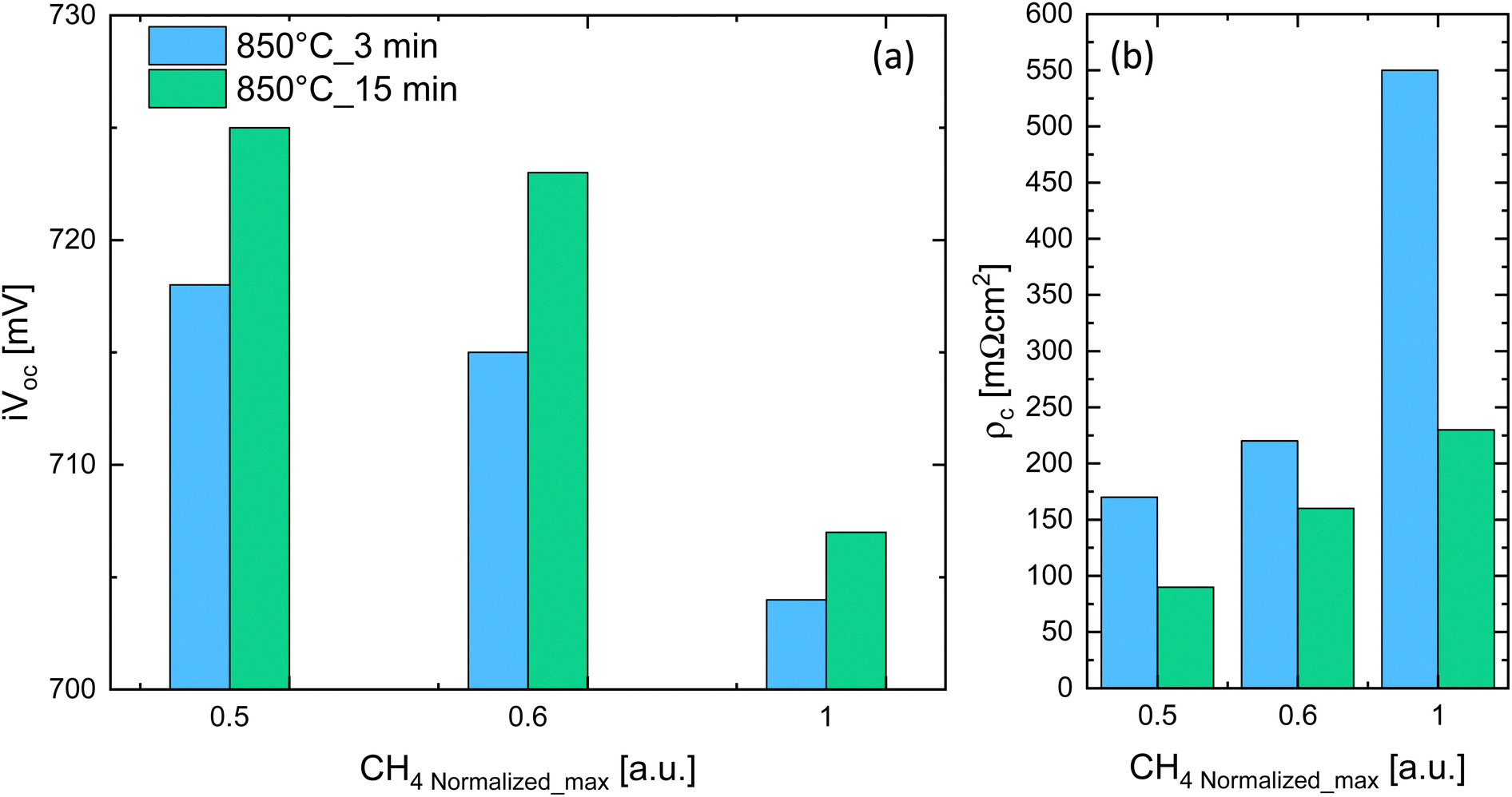 | ||
| Fig. 1 (a) Implied open circuit voltage (iVOC) and (b) specific contact resistance (ρc) as a function of the CH4 flow normalized to the maximum value (CH4/CH4max), CH4Normalized_max. The SiCx(p) is deposited here on both sides of textured wafers. | ||
The decrease in iVOC and increase in ρc towards higher CH4 flows is explained by the higher amount of C that can disrupt the interfacial SiOx and lowers B-doping incorporation for films richer in C.25,26 We hypothesize that the lower iVOC and higher ρc for annealing dwell time of 3 min compared to 15 min (for the same normalized CH4 flow) is explained by a shallower B in-diffused region into the c-Si wafer.12,14,17,27–31 Rear-side textured HTPC bottom cells were processed on single-side textured FZ p-type wafers (4′′) of the same thickness and base resistivity as the symmetrical samples. On the rear-side, the above-optimized SiCx(p) was deposited while a SiCx(n) as reported by Ingenito et al.25 was used for the front planar side. After stripping in HF of the SiNx:H used to hydrogenate the contact, iVOC values up to 723 mV are obtained on p-type wafers.
Taking advantage of the superior passivating properties of this new p-contact on textured c-Si wafers, PK/Si tandems were fabricated. Fig. 2(a) shows schematically the perovskite/Si HTPC device. Following the stripping of the SiNx, the ITO/Ag back electrode was created by sputtering. For the monolithic interconnection of the tandem sub-cells, a 10 nm-thin ITO recombination junction was sputtered onto the front SiCx(n) through a shadow mask. The top cell absorber had a composition of Cs0.17FA0.83Pb(I0.83Br0.17)3, corresponding to a bandgap of 1.63 eV. Interface recombination plays a significant role in perovskite solar cells, affecting both ideality factor and VOC.32 Similar to Al-Ashouri et al.,33 we employ a self-assembled monolayer (SAM) made of Me-4PACz as the hole transport layer (HTL), enabling excellent interface passivation and hole selectivity. A wetting layer made of SiOx nanoparticles was added. On the Electron transport layer (ETL) side, a thin layer of LiF is thermally evaporated between the perovskite and the C60 ETL. It is to be noted that the perovskite absorber was deposited on the full area of the 4′′ Si wafer, with each 4 cm2 tandem being then defined by the deposition of the front ITO electrode through a 7-cell metal mask. A Ag paste was then screen-printed at low temperature to metallize the cell,24 before depositing a LiF antireflective coating (ARC). Fig. 2(b) shows a picture of the 7 tandem cells on a 4′′ wafer.
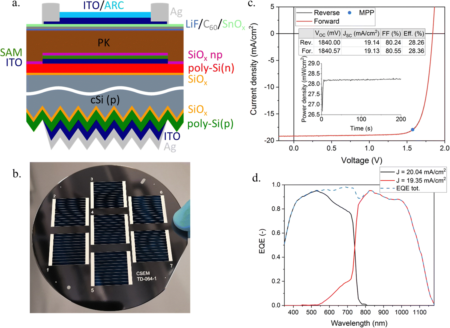 | ||
| Fig. 2 (a) Schematic view of the tandem cell stack. (b) Image of 7 tandem cells on a 4” wafer. The metallization is done by screenprinting. (c) Current–voltage (JV) characteristics of the best performing 4 cm2 cell. The inset table shows the JV parameters of the reverse (VOC → JSC, black) and forward (JSC → VOC, red) scans. The inset graph provides the maximum power point (MPP) tracking over 200 s, showing a steady-state efficiency of 28.25%. (d) External quantum efficiency (EQE) spectra of the top perovskite (black) and bottom Si HTPC (red) sub-cells. The blue dashed line shows the sum of the two. | ||
The current–voltage (JV) characteristics of the tandem cells were measured using a calibrated two-lamp solar simulator. The JV curve of the best device is displayed in Fig. 2(c). The cell was measured in the reverse (from VOC to JSC) and in the forward (from JSC to VOC) directions, highlighting a negligible hysteresis in these scan rate conditions (0.19 V s−1). The reverse JV measurement yields a VOC of 1840 mV, a JSC of 19.14 mA cm−2 and a Fill factor (FF) of 80.24%, resulting in a PCE of 28.26%, a value on par with record values reported with 4 cm2 perovskite/SHJ cells.34 This result is confirmed by a maximum power point tracking (MPP) over 200 s, which converges to a maximum power density of 28.25 mW cm−2 (average power over the last 60 s of tracking), as can be seen in the inset of Fig. 2(c). Fig. 2(d) shows the EQE measurement of the two sub-cells. From the integrated current density, one can infer that, with a top cell current of 20.04 mA cm−2 and a bottom cell current of 19.35 mA cm−2, the tandem device power output is limited by the bottom cell current, which may hence explain the high FF of the device35 (>80%). The monochromatic light spot of the EQE measurement is focused between the silver lines of the front metallization, thus excluding shadow losses and hence explaining the discrepancy with the Jsc from the JV curve. Fig. S1 of the ESI† shows the distribution of the JV parameters across the 4′′ Si wafer, demonstrating the good uniformity over a large area.
Thanks to the scalability of the different techniques involved – and notably of the metallization, we have successfully upscaled the process for perovskite/silicon tandem devices to a 4′′ pseudo-square with an active area of 57.4 cm2. The device exhibited a PCE of 22.51%. The perovskite layer and the front grid metallization were deposited using the same deposition approach as for the small area devices. These results demonstrate the potential for further optimization and scaling of perovskite/silicon tandem devices. This result is summarized in Fig. S2 (ESI†).
To conclude, we report here a perovskite/Si tandem solar cell based on a both-side passivating contact bottom cell architecture with a poly-Si(p) passivating contact deposited on the textured rear-side of the Si cell. This device reaches a power conversion efficiency of 28.25% on an active area of 4 cm2, in part thanks to a FF above 80%. These results demonstrate that Si cells based on HTPC, a category of contacts that is gaining traction on the PV market, can be combined with a perovskite top cell to reach efficiencies comparable to these reached with perovskite/SHJ tandems, and are also scalable to larger active area than those typically reported in the literature (1 cm2).
Author contributions
A. W. and A. I.: conceptualization, data curation, formal analysis, investigation, methodology, validation, visualization, writing – original draft; P.W.: investigation and resources; B. A. K., S.-J. M. J. J. D.L., C. A. and A. D.: conceptualization, investigation, methodology, validation; S. N and Q. J.: funding acquisition, project administration and supervision; C. B.: supervision. All: writing – review and editing.Conflicts of interest
There are no conflicts to declare.Acknowledgements
Part of the work presented here has received funding from the European Union's Horizon 2020 research and innovation program under Grant Agreement No. 861985 (project PeroCUBE), and from the Swiss National Science Foundation (SNSF) in the framework of the project PAPET (200021_197006).Notes and references
- NREL, Best Res. Effic. Chart.
- X. Y. Chin, D. Türkay, J. Steele, S. Tabean, S. Eswara, M. Mensi, P. Fiala, C. M. Wolff, A. Paracchino, K. Artuk, D. Jacobs, Q. Guesnay, F. Sahli, G. Andreatta, M. Boccard, Q. Jeangros and C. Ballif, Interface passivation for 31.25%-efficient perovskite/silicon tandem solar cells, Science, 2023, 59–63 CrossRef CAS PubMed , in print.
- S. Mariotti, E. Köhnen, F. Scheler, K. Sveinbjörnsson, L. Zimmermann, M. Piot, F. Yang, B. Li, J. Warby, A. Musiienko, D. Menzel, F. Lang, S. Keßler, I. Levine, D. Mantione, A. Al-Ashouri, M. S. Härtel, K. Xu, A. Cruz, J. Kurpiers, P. Wagner, H. Köbler, J. Li, A. Magomedov, D. Mecerreyes, E. Unger, A. Abate, M. Stolterfoht, B. Stannowski, R. Schlatmann, L. Korte and S. Albrecht, Interface engineering for high-performance, triple-halide perovskite–silicon tandem solar cells, Science, 2023, 381, 63–69 CrossRef CAS PubMed.
- F. Fu, J. Li, T. C. Yang, H. Liang, A. Faes, Q. Jeangros, C. Ballif and Y. Hou, Monolithic Perovskite-Silicon Tandem Solar Cells: From the Lab to Fab?, Adv. Mater., 2022, 34, 2106540 CrossRef CAS PubMed.
- A. Al-Ashouri, E. Köhnen, B. Li, A. Magomedov, H. Hempel, P. Caprioglio, J. A. Márquez, A. B. M. Vilches, E. Kasparavicius, J. A. Smith, N. Phung, D. Menzel, M. Grischek, L. Kegelmann, D. Skroblin, C. Gollwitzer, T. Malinauskas, M. Jošt, G. Matič, B. Rech, R. Schlatmann, M. Topič, L. Korte, A. Abate, B. Stannowski, D. Neher, M. Stolterfoht, T. Unold, V. Getautis and S. Albrecht, Monolithic perovskite/silicon tandem solar cell with >29% efficiency by enhanced hole extraction, Science, 2020, 370, 1300–1309 CrossRef CAS PubMed.
- Cell, KAUST claims 33.7% efficiency for perovskite/silicon tandem solar, https://www.pv-magazine.com/2023/05/30/kaust-claims-33-7-efficiency-for-perovskite-silicon-tandem-solar-cell/.
- K. Sveinbjörnsson, B. Li, S. Mariotti, E. Jarzembowski, L. Kegelmann, A. Wirtz, F. Frühauf, A. Weihrauch, R. Niemann, L. Korte, F. Fertig, J. W. Müller and S. Albrecht, Monolithic Perovskite/Silicon Tandem Solar Cell with 28.7% Efficiency Using Industrial Silicon Bottom Cells, ACS Energy Lett., 2022, 7, 2654–2656 CrossRef.
- S. Mariotti, K. Jäger, M. Diederich, M. S. Härtel, B. Li, K. Sveinbjörnsson, S. Kajari-Schröder, R. Peibst, S. Albrecht, L. Korte and T. Wietler, Monolithic Perovskite/Silicon Tandem Solar Cells Fabricated Using Industrial p-Type Polycrystalline Silicon on Oxide/Passivated Emitter and Rear Cell Silicon Bottom Cell Technology, Sol. RRL, 2022, 6, 2101066 CrossRef CAS.
- VDMA, International Technology Roadmap for Photovoltaic, 2022, vol. 13th Edition.
- Y. Wu, P. Zheng, J. Peng, M. Xu, Y. Chen, S. Surve, T. Lu, A. D. Bui, N. Li, W. Liang, L. Duan, B. Li, H. Shen, T. Duong, J. Yang, X. Zhang, Y. Liu, H. Jin, Q. Chen, T. White, K. Catchpole, H. Zhou and K. Weber, 27.6% Perovskite/c-Si Tandem Solar Cells Using Industrial Fabricated TOPCon Device, Adv. Energy Mater., 2022, 12, 2200821 CrossRef CAS.
- Z. Ying, Z. Yang, J. Zheng, H. Wei, L. Chen, C. Xiao, J. Sun, C. Shou, G. Qin, J. Sheng, Y. Zeng, B. Yan, X. Yang and J. Ye, Monolithic perovskite/black-silicon tandems based on tunnel oxide passivated contacts, Joule, 2022, 6, 1–18 CrossRef.
- G. Nogay, F. Sahli, J. Werner, R. Monnard, M. Boccard, M. Despeisse, F.-J. Haug, Q. Jeangros, A. Ingenito and C. Ballif, 25.1%-Efficient monolithic perovskite/silicon tandem solar cell based on a p-type monocrystalline textured silicon wafer and high-temperature passivating contacts, ACS Energy Lett., 2019, 4, 844–845 CrossRef CAS.
- U. Römer, R. Peibst, T. Ohrdes, B. Lim, J. Krügener, E. Bugiel, T. Wietler and R. Brendel, Recombination behavior and contact resistance of n+ and p+ poly-crystalline Si/mono-crystalline Si junctions, Sol. Energy Mater. Sol. Cells, 2014, 131, 85–91 CrossRef.
- M. Lozac’h, S. Nunomura, H. Sai and K. Matsubara, Passivation property of ultrathin SiOx:H/a-Si:H stack layers for solar cell applications, Sol. Energy Mater. Sol. Cells, 2018, 185, 8–15 CrossRef.
- F. Feldmann, R. Müller, C. Reichel and M. Hermle, Ion implantation into amorphous Si layers to form carrier-selective contacts for Si solar cells, Phys. Status Solidi RRL, 2014, 08, 767–770 CrossRef CAS.
- F. Feldmann, M. Simon, M. Bivour, C. Reichel, M. Hermle and S. W. Glunz, Carrier-selective contacts for Si solar cells, Appl. Phys. Lett., 2014, 104, 181105 CrossRef.
- U. Römer, R. Peibst, T. Ohrdes, B. Lim, J. Krügener, T. Wietler and R. Brendel, Ion implantation for poly-Si passivated back-junction back-contacted solar cells, IEEE J. Photovoltaics, 2015, 5, 507–514 Search PubMed.
- D. L. Young, W. Nemeth, V. LaSalvia, R. Reedy, S. Essig, N. Bateman and P. Stradins, Interdigitated Back Passivated Contact (IBPC) Solar Cells Formed by Ion Implantation, IEEE J. Photovoltaics, 2016, 6, 41–47 Search PubMed.
- C. Reichel, F. Feldmann, R. Müller, R. C. Reedy, B. G. Lee, D. L. Young, P. Stradins, M. Hermle and S. W. Glunz, Tunnel oxide passivated contacts formed by ion implantation for applications in silicon solar cells, J. Appl. Phys., 2015, 118, 205701 CrossRef.
- D. Yan, A. Cuevas, J. Bullock, Y. Wan and C. Samundsett, Phosphorus-diffused polysilicon contacts for solar cells, Sol. Energy Mater. Sol. Cells, 2015, 142, 75–82 CrossRef CAS.
- A. Ingenito, G. Nogay, J. Stuckelberger, P. Wyss, L. Gnocchi, C. Allebe, J. Horzel, M. Despeisse, F.-J. Haug, P. Loper and C. Ballif, Phosphorous-Doped Silicon Carbide as Front-Side Full-Area Passivating Contact for Double-Side Contacted c-Si Solar Cells, IEEE J. Photovoltaics, 2019, 9, 346–354 Search PubMed.
- Y. Larionova, M. Turcu, S. Reiter, R. Brendel, D. Tetzlaff, J. Krügener, T. Wietler, U. Höhne, J.-D. Kähler and R. Peibst, On the recombination behavior of p+ -type polysilicon on oxide junctions deposited by different methods on textured and planar surfaces, Phys. Status Solidi, 2017, 1700058 CrossRef.
- M. Stodolny, K. Tool, B. Geerligs, J. Loffler, A. Weeber, Y. Wu, J. Anker, X. Lu, J. Liu, P. Bronsveld, A. Mewe, G. Janssen and G. Coletti, PolySi Based Passivating Contacts Enabling Industrial Silicon Solar Cell Efficiencies up to 24%, Conf. Rec. IEEE Photovolt. Spec. Conf., 2019, 1456–1459 Search PubMed.
- B. A. Kamino, B. Paviet-Salomon, S.-J. Moon, N. Badel, J. Levrat, G. Christmann, A. Walter, A. Faes, L. Ding, J. J. Diaz Leon, A. Paracchino, M. Despeisse, C. Ballif and S. Nicolay, Low-Temperature Screen-Printed Metallization for the Scale-Up of Two-Terminal Perovskite-Silicon Tandems, ACS Appl. Energy Mater., 2019, 2, 3815–3821 CrossRef CAS.
- A. Ingenito, G. Nogay, J. A. Stückelberger, P. Wyss, J. Horzel, C. Allebé, M. Despeisse, F.-J. Haug, P. Löper and C. Ballif, in 33rd European Photovoltaic Solar Energy Conference and Exhibition (EU PVSEC), Amsterdam, 2017.
- A. Ingenito, G. Nogay, Q. Jeangros, E. Rucavado, C. Allebé, S. Eswara, N. Valle, T. Wirtz, J. Horzel and T. Koida, A passivating contact for silicon solar cells formed during a single firing thermal annealing, Nat. Energy, 2018, 3, 800 CrossRef CAS.
- G. Nogay, J. Stuckelberger, P. Wyss, E. Rucavado, C. Allebé, T. Koida, M. Morales-masis, M. Despeisse, F. Haug, P. Löper and C. Ballif, Interplay of annealing temperature and doping in hole selective rear contacts based on silicon-rich silicon-carbide thin fi lms, Sol. Energy Mater. Sol. Cells, 2017, 173, 18–24 CrossRef CAS.
- M. Lehmann, N. Valle, J. Horzel, A. Pshenova, P. Wyss, M. Döbeli, M. Despeisse, S. Eswara, T. Wirtz, Q. Jeangros, A. Hessler-wyser, F. Haug, A. Ingenito, C. Ballif, E. Polytechnique, F. De Lausanne, M. Imt, T. Film and R. D. La Maladière, Analysis of hydrogen distribution and migration in fired passivating contacts, Sol. Energy Mater. Sol. Cells, 2019, 200, 110018 CrossRef CAS.
- G. Yang, A. Ingenito, N. Van Hameren, O. Isabella and M. Zeman, Design and application of ion-implanted polySi passivating contacts for interdigitated back contact c-Si solar cells, Appl. Phys. Lett., 2016, 108, 033903 CrossRef.
- H. Steinkemper, F. Feldmann, M. Bivour and M. Hermle, Theoretical Investigation of Carrier-selective Contacts Featuring Tunnel Oxides by Means of Numerical Device Simulation, Energy Procedia, 2015, 77, 195–201 CrossRef CAS.
- P. Procel, P. Löper, F. Crupi, C. Ballif and A. Ingenito, Numerical simulations of hole carrier selective contacts in p-type c-Si solar cells, Sol. Energy Mater. Sol. Cells, 2019, 200, 109937 CrossRef CAS.
- P. Caprioglio, C. M. Wolff, O. J. Sandberg, A. Armin, B. Rech, S. Albrecht, D. Neher and M. Stolterfoht, On the Origin of the Ideality Factor in Perovskite Solar Cells, Adv. Energy Mater., 2020, 10, 1–9 Search PubMed.
- A. Al-Ashouri, E. Köhnen, B. Li, A. Magomedov, H. Hempel, P. Caprioglio, J. A. Márquez, A. B. Morales Vilches, E. Kasparavicius, J. A. Smith, N. Phung, D. Menzel, M. Grischek, L. Kegelmann, D. Skroblin, C. Gollwitzer, T. Malinauskas, M. Jošt, G. Matič, B. Rech, R. Schlatmann, M. Topič, L. Korte, A. Abate, B. Stannowski, D. Neher, M. Stolterfoht, T. Unold, V. Getautis and S. Albrecht, Monolithic perovskite/silicon tandem solar cell with >29% efficiency by enhanced hole extraction, Science, 2020, 370, 1300–1309 CrossRef CAS PubMed.
- D. Kirk, tandemPV Workshop, Freiburg, 2022 Search PubMed.
- M. Boccard and C. Ballif, Influence of the Subcell Properties on the Fill Factor of Two-Terminal Perovskite–Silicon Tandem Solar Cells, ACS Energy Lett., 2020, 5, 1077–1082 CrossRef CAS.
Footnotes |
| † Electronic supplementary information (ESI) available: Fabrication details, device characterization, large area tandems. See DOI: https://doi.org/10.1039/d3ya00048f |
| ‡ Current address: Institut Interdisciplinaire d’Innovation Technologique (3IT), Sherbrooke University, Sherbrooke, Canada. |
| This journal is © The Royal Society of Chemistry 2023 |