Enhancing the optoelectronic properties of solution-processed AgInSe2 thin films for application in photovoltaics†
Shubhanshu
Agarwal
 a,
Kyle
Weideman
a,
David
Rokke
a,
Kyle
Weideman
a,
David
Rokke
 a,
Kiruba Catherine
Vincent
 a,
Dmitry
Zemlyanov
 b and
Rakesh
Agrawal
 *a
*a
aDavidson School of Chemical Engineering, Purdue University, West Lafayette, Indiana 47907, USA. E-mail: agrawalr@purdue.edu
bBirck Nanotechnology Center, Purdue University, West Lafayette, Indiana 47907, USA
First published on 7th December 2023
Abstract
AgInSe2 is a promising direct bandgap thin-film material with a rare n-type conductivity. Similar to thin film photovoltaic materials such as Cu(In,Ga)Se2 (CIGSe), which have achieved efficiencies as high as ∼23%, AgInSe2 also crystallizes in a chalcopyrite phase while also being more tolerant to antisite defects due to higher defect formation energies resulting from more significant variations in cation sizes. AgInSe2 has a suitable bandgap of 1.24 eV, which lies in the high-efficiency region of the detailed balance limit. In this work, we have utilized a dimethyl formamide–thiourea–chloride-based solution-processed route to deposit a thin film of AgInS2 which is converted into AgInSe2 after a heat-treatment step in a selenium environment. We observed that AgInSe2 optoelectronic properties depend on the Ag/In ratio and the selenium heat-treatment conditions. Significant improvements in photoluminescence yield and lifetime are observed for Ag-poor films in selenium-rich conditions. X-ray photoelectron spectroscopy (XPS) measurements confirm a higher amount of selenium on the surface of films with improved optoelectronic properties. Furthermore, a high minority carrier lifetime of 9.2 ns and a photoluminescence quantum yield (PLQY) of 0.013% are obtained without any passivating layer, which improved to 0.03% after CdS passivation. Hall effect measurements confirm that AgInSe2 has n-type conductivity with a moderate carrier concentration (10−14 cm−3), more suitable for a p–i–n architecture. XPS has further confirmed the moderate n-type conductivity.
Introduction
Inorganic semiconductors find utility in various optoelectronic applications ranging from photovoltaics to telecommunications, lighting, sensors, medical devices and others.1–9 For the worldwide use of solar energy to lead to a green energy economy, we need photovoltaic materials that are low-cost, stable, have good optoelectronic and charge transport properties, and can be easily manufactured on a large scale. Thin-film solar cells show all these characteristics, some of which have surpassed the monocrystalline Si efficiency.10 Among thin-film devices, CdTe and CuInSe2/Cu(In,Ga)Se2 (CISe/CIGSe) are among the most promising. CIGSe has achieved a lab-record efficiency of 23.35% and can be produced by solution processing techniques.11–13 However, the propensity of copper cations to exist in two oxidation states results in lower formation energy for copper-based defects in the CIGSe crystal lattice.14–16 Replacing copper with silver in CISe may be helpful as Ag only has a +1 oxidation state and has a larger cation size than In+3 and Ga+3, significantly increasing the defect formation energy.17,18 CISe, however, has a bandgap of 1.0 eV, which is not suited for single-junction PV applications, whereas AgInSe2 has a larger bandgap of 1.24 eV, closer to the ideal 1.4 eV bandgap predicted by the detailed balance limit.19–21 AgInSe2 is also thermodynamically stable and has good electronic properties.22–24 It is n-type, which is different from CISe/CIGSe, but the structural similarities with CIGSe could be a good sign for the viability of this material. All these favorable properties of silver addition have warranted a need to study AgInSe2 in detail. However, there is only one instance in literature where a solar device has been fabricated from AgInSe2. Agel et al. grew an n-type AgInSe2 film on a p-type Si substrate.25 They achieved a conversion efficiency of 2.71%, and the device showed Schottky diode-like characteristics. These numbers look promising for a material that has been scarcely studied and optimized.In most cases, AgInSe2 films have been prepared using costly vacuum processing techniques.20,23–30 These techniques require a high vacuum, have inefficient material utilization, and involve batch processing.31,32 Solution processing is a cost-effective alternative for rapidly commercializing promising materials such as AgInSe2. It works at ambient pressure conditions, has a more efficient material utilization, and can be used in the roll-to-roll manufacturing of thin-film absorber films.33 However, in the literature, there are no reports of a solution-processed AgInSe2 film other than a recent PhD thesis.34 Limited research has been done on AgInSe2 despite its promising properties. Hence, our research goal is to fabricate a solution-processed AgInSe2 film with good optoelectronic properties for incorporation into a solar cell.
Hence, this work aims to fabricate and characterize solution-processed AgInSe2 films for their potential use in solar cells. We have utilized the benign N-N dimethyl formamide (DMF)–thiourea (TU)–chlorides chemistry to cast AgInS2 thin film, which is further heat-treated in a selenium environment to form AgInSe2 film. We have optimized the composition and selenization conditions to lower the defects in AgInSe2 films and achieved high photoluminescence quantum yield (PLQY). We have further done advanced characterizations to evaluate the electrical properties and the band positions.
Experimental
Materials
Silver(I) chloride (99.999%), indium(III) chloride (99.999%), thiourea (99.98%), N-N dimethylformamide (>99.8%), butylamine (>99.5%), 1,2-ethanedithiol (>99%), alumina dispersed in 2-propanol (20 wt%), and SeCl4 were obtained from Sigma Aldrich. Selenium used in selenization (5 mm pellets, 99.999%) and selenium powder (99.99%) were obtained from Millipore Sigma. All chemicals were used as received except for the thiourea, which was twice recrystallized from 18.2 MΩ deionized water and dried under vacuum, followed by an ambient-pressure drying in the air overnight at 90 °C.Corning's alkali-free Eagle XG (EXG) glass substrates were obtained from Stemmerich. All chemicals were stored in nitrogen-filled glove boxes.
Ink preparation
Ink preparation was performed in a nitrogen-filled glove box. DMF–TU–chlorides chemistry was utilized to prepare the molecular precursor ink, which uses AgCl and InCl3 as the Ag and In metal precursors. Since AgCl is photosensitive, it was always handled in the dark. In most experiments, 0.8 M total metal concentration was maintained in ink, and the Ag/In ratio was varied. Moreover, 1.6 M TU concentration was maintained in DMF, and AgCl and InCl3 were sequentially added to the TU + DMF solution to prepare the ink. The ink was then vortexed and stirred on a heated stir plate at 35 °C. Before coating, the ink was filtered with a 0.45-micron pore-sized PTFE membrane syringe filter.A 1.2 M total metal concentration ink was also used with a 3.8 M TU concentration to achieve a relatively thick film.
Molybdenum and alumina deposition
Before molybdenum or alumina deposition, EXG glass was thoroughly rinsed with DI water, 2-propanol, and methanol and then sonicated in an Alconox bath followed by sonication in DI water. The glass was then cleaned in a UV-ozone cleaner for 30 min. The glass was loaded in a PVD chamber for molybdenum deposition and 800 nm thick molybdenum layer was sputtered at an ultralow vacuum.For film growth on alumina-coated glass, the alumina nanoparticles solution was initially diluted by combining 0.2 ml of commercial alumina solution with 1.8 ml 2-propanol. The solution was then spin-coated on the cleaned EXG glass at 1000 rpm for 1 min, followed by 1 min annealing at 100 °C and 30 min annealing at 500 °C.
Film coating
The DMF–thiourea–chlorides ink was coated on a molybdenum or alumina-coated EXG glass substrate (which contains no sodium) to fabricate AgInS2 thin films. Unless specified, the film is coated on molybdenum in this report. The coating procedure was performed on an automated spin coater in a nitrogen-filled glove box. 200 μl of ink was used in each cycle with the substrate holder rotating at 3000 rpm for 30 seconds, followed by a 30 second wait time for the ink to dry. The sample was then transferred to a hot plate set at 300 °C, and the film was annealed for 90 seconds. The film was then cooled on an aluminum block. This coating cycle was repeated 14 times with 0.8 M total metal concentration ink to achieve a film of the desired thickness. 10 coating cycles with 1000 rpm were used instead with an ink of 1.2 M total metal concentration to achieve thicker films.Regular selenization
The next step involved annealing the sulfide AgInS2 film in a selenium environment in a refractory tube furnace following the procedure for selenization of Cu(In,Ga)S2 films.35 In a regular selenization setup, the sample rested on the floor of a graphite box with selenium pellets arranged around it, as shown in Fig. 1a. Before ramping up the temperature, the tube furnace was purged multiple times through vacuum and argon cycles to remove the oxygen. Then, the furnace temperature was ramped up to the desired setpoint (475–600 °C), and the film was annealed in a selenium environment for 20 minutes.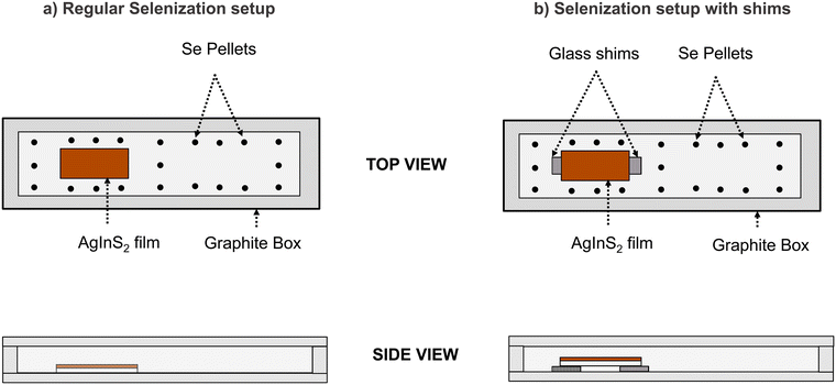 | ||
| Fig. 1 Schematic showing the difference between the (a) regular selenization setup and the (b) selenization setup with shims. | ||
Modified selenization with glass shims
A modified selenization setup was used to increase the selenium supply to the film during the heat-up period. In this setup, the sample rested on two small pieces of EXG glass near the far edges of the 1′′ × 0.5′′ film, shown in Fig. 1b. This arrangement avoided any direct contact of the sample with the graphite box, which has high absorptivity and thermal conductivity and thus quickly heats the sample if it rests directly on the graphite surface. However, the selenium pellets were still in contact with the graphite floor and volatilized normally, the volatility rate set by the graphite floor temperature. The sulfide film heated up slowly because of increased thermal resistance from the glass shims, resulting in a significant difference in temperature between the selenium vapors and the film's surface, causing higher selenium condensation onto the film. Hence, this modified setup had more liquid Se on the film. Simplified numerical heat transfer calculations in Fig. S1 and S2 (ESI†) and Weidemann's doctoral thesis support the above discussion.36Other selenization methods
Other selenization methods with higher selenium availability were also employed. In the first case, an additional 0.4 M selenium ink in butylamine + 1,2-ethanedithiol was prepared, and two layers of this ink were coated on top of the AgInS2 film. The film was then annealed at 100 °C for two minutes to remove the solvents. This provided a thick layer of Se on the AgInS2 film that could act as a selenium source during selenization. This modified film was further selenized by regular selenization (no shims used). In another method, 25 mg selenium powder was spread on the AgInS2 film, which also acted as the selenium source during selenization. This film was also selenized via regular selenization.CdS deposition
CdS was deposited using chemical bath deposition as reported elsewhere.37Characterization
Raman spectroscopy was performed using a Horiba/Jobin-Yvon HR800 Raman spectrometer with a 632.8 nm excitation laser wavelength. A quartz cuvette enclosed in a nitrogen atmosphere was used for collecting spectra on liquid solutions. X-ray diffraction was performed in a Rigaku SmartLab Diffractometer under ambient conditions in parallel beam geometry with an incident beam angle of 0.5 degrees using a Cu Kα source (λ = 1.5406 Å) operating at 40 kV and 44 mA. Hall effect measurements were performed on a LakeShore M91 FastHall with magnetic field strengths from −9 Tesla to 9 Tesla.Time-resolved photoluminescence (TRPL) was acquired by the single photon counting technique using a 640 nm diode laser (pulse width of 100 ps, 1 MHz) and an InGaAs photomultiplier tube (Hamamatsu H10330-75). The obtained TRPL decay curves were fitted with biexponential fits, and the statistical average of the lifetime values was reported. The statistical average is given by:
Photoluminescence measurements were performed with a Horiba LabRAM HR800 using a 632.8nm He:Ne laser and a liquid nitrogen-cooled InGaAs detector. Spectral corrections were performed by comparing the normalized measured spectrum of a calibrated light source (Avantes Avalight HAL-CAL MINI) with the known normalized spectrum provided by the vendor, as detailed in a previous report.38 Further apparatus calibration was performed to obtain quantitative photoluminescence, as detailed in Rokke's doctoral thesis.34
The XPS data was obtained at the Surface Analysis Facility of the Birck Nanotechnology Center, Purdue University. X-ray photoelectron spectroscopy (XPS) measurements were performed using a Kratos Axis Ultra DLD imaging XPS instrument with a monochromatic Al Kα (1486.6 eV) radiation and a chamber pressure of less than 2 × 10⁻⁹ Torr. The samples were transferred immediately to an argon-filled glovebox after selenization to avoid oxygen contamination and were then vacuum sealed to transfer to the XPS instrument. The vacuum seal was broken inside a glovebox connected to the XPS instrument. For the XPS data analysis CASAXPS software was used. The data was charge corrected using the C1s peak set at 284.8 eV.
Scanning electron microscopy (SEM) measurements were performed on the FEI Quanta three-dimensional system with an Everhart–Thornley detector at an accelerating voltage of 7 kV with a working distance of 10 mm.
Fisher XAN 250 X-ray fluorescence (XRF) instrument at 50 kV voltage with a primary Ni filter containing a silicon drift detector was used to measure the bulk composition. We have reported XRF-measured composition rather than the nominal composition in this work.
Reflectance data was acquired using a PerkinElmer Lambda 950 spectrometer with an integrating sphere.
Results and discussions
Solution-processed AgInSe2
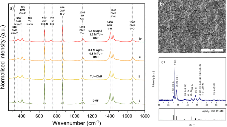
In the only reported case of solution-processed AgInSe2 film, Ag2S and In as the metal precursors were dissolved in butylamine and 1,2-ethanedithiol to prepare a stable ink.34 However, this approach had some challenges: (a) the films had a poor PL yield, (b) their minority carrier lifetime was low at around 300 ps, and (c) the amines and thiols are toxic.All the above challenges motivated us to search for other benign chemistries. We explored the DMF–thiourea–chlorides route, which is reported to produce carbon-free CuInSe2 thin films.16 DMF, a Lewis basic aprotic solvent, cannot solvate monovalent cations, such as Ag+, on its own. However, adding TU stabilizes the Ag+ cation, and the solubility of AgCl increases when at least two mol of TU are present per mol of AgCl. The 0.4 M AgCl with 0.4 M TU in DMF did not dissolve. However, 0.4 M AgCl dissolved completely with 0.8 M and higher TU concentrations in DMF. Liquid Raman measurements verify an interaction of AgCl and TU owing to the gradual peak broadening and peak shift of the 744 cm−1 C![[double bond, length as m-dash]](https://www.rsc.org/images/entities/char_e001.gif) S stretch, as shown in Fig. 2a. Thiourea also increases the solubility of InCl3 by reacting with the free Cl− in the solution and increasing the concentration of highly soluble [InCl]2+ species.16Fig. 2b shows the as-coated AgInS2 films from the equimolar AgCl and InCl3 ink which form densely packed flower-shaped grains via this route and showed the orthorhombic phase as opposed to the chalcopyrite phase observed in the literature at these temperatures, see Fig. 2c. Surprisingly, the as-coated film showed an intense PL emission with a broad spectrum centered at 1.18 eV, possibly originating from a midgap defect in AgInS2 or some secondary phases, as evidenced by Fig. S3 (ESI†). We performed the variable temperature photoluminescence (PL) for the as-coated AgInS2 film at 150 K and 77 K and observed the similar midgap peak with increased intensity as the measurement temperature reduced (see Fig. S4, ESI†). We also observed a slight blue shift in the midgap PL peak position as the temperature reduced. However, still more work is required on assigning this peak as the room-temperature PL peak position changes slightly from one spot to another varying between 1.17 to 1.25 eV, as shown in Fig. S5 (ESI†).
S stretch, as shown in Fig. 2a. Thiourea also increases the solubility of InCl3 by reacting with the free Cl− in the solution and increasing the concentration of highly soluble [InCl]2+ species.16Fig. 2b shows the as-coated AgInS2 films from the equimolar AgCl and InCl3 ink which form densely packed flower-shaped grains via this route and showed the orthorhombic phase as opposed to the chalcopyrite phase observed in the literature at these temperatures, see Fig. 2c. Surprisingly, the as-coated film showed an intense PL emission with a broad spectrum centered at 1.18 eV, possibly originating from a midgap defect in AgInS2 or some secondary phases, as evidenced by Fig. S3 (ESI†). We performed the variable temperature photoluminescence (PL) for the as-coated AgInS2 film at 150 K and 77 K and observed the similar midgap peak with increased intensity as the measurement temperature reduced (see Fig. S4, ESI†). We also observed a slight blue shift in the midgap PL peak position as the temperature reduced. However, still more work is required on assigning this peak as the room-temperature PL peak position changes slightly from one spot to another varying between 1.17 to 1.25 eV, as shown in Fig. S5 (ESI†).
Fig. 3c indicates the as-coated stoichiometric orthorhombic AgInS2 film converted to chalcopyrite AgInSe2 film after selenization. We potentially accessed a selenium rich Ag-Se binary alloy liquid flux that helped nucleate and grow large AgInSe2 grains similar to those reported for other material systems.39–41 The selenized film has irregularly shaped grains when selenized with regular selenization conditions, as shown in Fig. 3a and b. Fig. S6 (ESI†) shows the film also has residual carbon. Different values have been reported in the literature for the bandgap of AgInSe2 ranging between 1.02 to 1.35 eV depending on the growth method and processing conditions.20,24,25,27,28,30,42–47 However, the photoluminescence for our film is centered at 1.25 eV with a narrow FWHM of 59 meV, shown in Fig. 3d. The bandgap was further confirmed by the Kubelka–Munk transformation on UV-vis-NIR diffuse reflectance measurement. The analysis in Fig. S7 (ESI†) shows that the optical bandgap of the film is 1.24 eV which is comparable to the photoluminescence peak position. The PLQY yield and the minority carrier lifetimes were poor for the stoichiometric film under all conditions of regular selenization with PLQY less than 1 × 10⁻⁴% and a lifetime less than 300 ps, shown in Fig. 3d and e. We tried selenizations at temperatures between 475 and 525 °C but saw no improvements. These results suggest the presence of intrinsic defects in the AgInSe2 fabricated under these conditions.
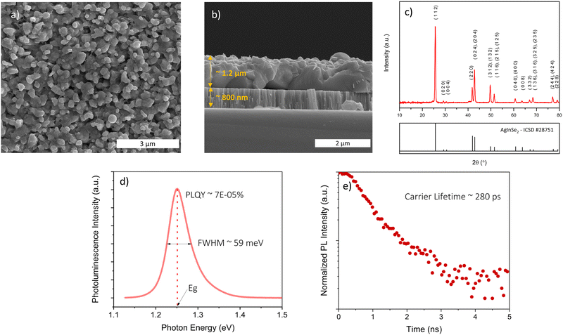 | ||
| Fig. 3 (a) SEM top-view, (b) SEM cross-sectional view, (c) XRD pattern, (d) photoluminescence plot, and (e) TRPL decay curve of stoichiometric AgInSe2 film selenized at 500 °C with regular selenization (arrangement shown in Fig. 1a). | ||
Effect of Ag/In ratio on the optoelectronic properties of AgInSe2
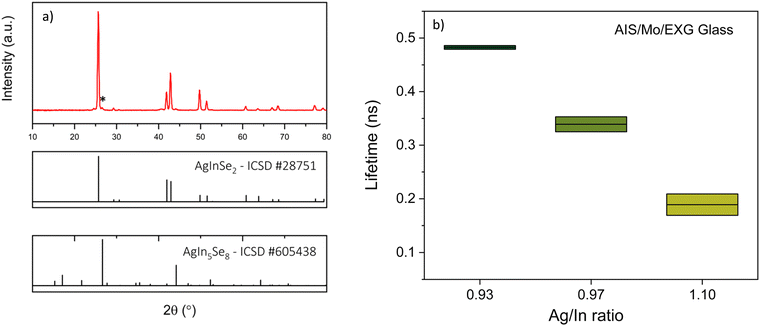
We also varied the Ag/In ratio in the solution-processed AgInSe2 films produced via the DMF–thiourea–chlorides chemistry to study its impact on optoelectronic properties. For Ag/In < 1 (Ag-poor), we observed slight improvements in PL and lifetime similar to CISe/CIGSe. These improvements continued for Ag/In as low as 0.9, where they started forming a secondary phase of AgIn5Se8, as shown in Fig. 4a. Although there was an improvement in PL and carrier lifetime, the numbers were still relatively low, as shown in Fig. 4b. These improvements were possibly due to the formation of benign defect complexes for Ag-poor films, such as 2VAg + InAg, similar to those reported for CuInSe2.48 While Ag poor AgInSe2 composition seems favorable, other defects may also limit the performance.Annealing AgInSe2 in Se rich atmosphere
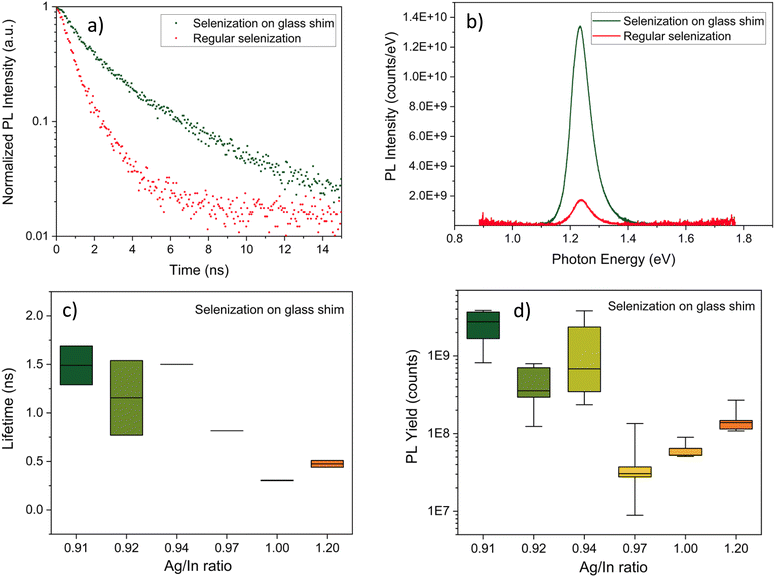
The published literature on AgInSe2/CuInSe2/Cu(In,Ga)Se2 has many instances of the detrimental effects of selenium vacancies on the absorber films. In a few cases, authors noted that growing AgInSe2 in a Se-deficient environment could harm the material's crystallinity and electronic properties. Ema et al. observed that the phase pure chalcopyrite AgInSe2 could only be produced when sufficient Se vapor was provided.49 Patel et al. found that the AgInSe2 films exhibited higher resistivity because of selenium deficiency.26 On similar grounds, Matsuo et al. pointed out that the AgInSe2 samples annealed above 400 °C contained Ag and Se vacancies (VAg and VSe, respectively).28 In CuInSe2, selenium vacancies act as donors and provide electrons to the conduction band; similar phenomena may happen for AgInSe2. In this regard, Abdel-Hady et al. noticed that the room temperature electron concentration varied between 1012–1018 cm−3 based on selenium deficiency for their n-type AgInSe2 film.23 Thus, it is apparent that growing AgInSe2 in a selenium-deficient environment could be deleterious.The above discussion points towards that VSe defects could potentially be harmful to the AgInSe2 absorber films. Hence, we hypothesized that the photoluminescence yield and minority carrier lifetime in solution-processed AgInSe2 would improve by increasing the selenium availability during selenization. Thus, our goal was to increase the selenium flux and maintain a selenium-rich environment during selenization to minimize defect formation while limiting the excess condensed selenium vapor on the final film.
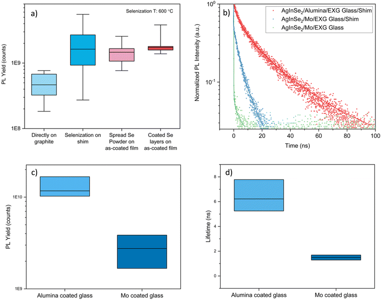
We used various means to incorporate increased selenium in the films to test our hypothesis. Methods include using glass shims as the support for the substrate to increase selenium condensation on the film (Fig. 1b), coating Se layers on top of as-coated AgInS2, and dusting Se powder on AgInS2 film before selenization. These methods are discussed in detail in the Experimental section.
Improvements in optoelectronic properties
The majority of literature noted AgInSe2 to be an n-type material. Moreover, similar to CuInSe2, VSe could be a deep donor defect in AgInSe2, which can act as recombination centers for minority carrier holes. If present in a high concentration, VSe could harm the optoelectronic properties. Hence, we focused on incorporating increased selenium in the film during selenization.| AgInSe2 selenized on graphite | AgInSe2 selenized on shim | |
|---|---|---|
| Surface composition (XPS) | Ag0.64In1Se1.2 | Ag0.52In1Se1.5 |
| Bulk composition (XRF) | Ag0.94In1Se2.3 | Ag0.92In1Se2.3 |
Continuous film formation
Till now, we have achieved excellent optoelectronic properties for AgInSe2 films, but the films are rather non-homogenous, as shown in Fig. S15–S18 (ESI†). They have large disconnected grains, possibly because of the excessive growth in the out-of-plane direction. Hence, there was a need to achieve a thicker film so that grains grow enough laterally and a continuous film is achieved. We achieved a relatively continuous film using shims after selenization when started with 1.2 M total metal concentration, coated 10 layers and selenized at 600 °C, as shown in Fig. 7a and b. However, we only achieved an estimated Voc of 700 mV for this film through PLQY analysis, which was slightly lower than the films selenized at lower temperatures. This is partially due to the inability to maintain a saturated selenium environment at 600 °C for 20 min due to the high vapor pressure of selenium and, therefore, increased selenium leakage rate from the box during annealing and cool down. We again connect this to the selenium-based defects. The grain size improved upon selenization at higher temperatures, which should have reduced the grain boundary recombination, but some other defects seem to affect the performance of higher-temperature films. We hypothesize that increased selenium loss from the film at higher temperatures could limit the performance. In other words, selenium vacancies were possibly formed in AgInSe2 film by selenizing at higher temperatures in an insufficient selenium environment and during cooldown. Nonetheless, we again passivated this film with a 50 nm thick layer of CdS, and it improved the Voc to 741 mV with a PLQY of 0.019%.Electrical characterizations
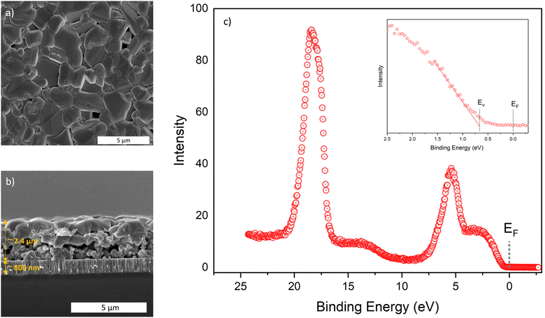
These has been a lack of consensus on the electrical properties of AgInSe2 in the literature. Both p-type and n-type conductivity has been suggested for AgInSe2 with carrier concentrations varying from intrinsic to 1018 cm−3. Similar large variations have also been reported for the conductivity and the carrier mobility.23,24,26–28,30,44–46,49 These variations might be due to the different defects being present in the material depending on the composition. It is possible that the selenium vacancies are contributing to the n-type conductivity and a selenium poor composition may lead an n-type conductivity with high electron concentration. Other possibility is that InAg defect might be a shallow donor defect and could be contributing electrons to the conduction band, although more work is needed to confirm this. Similarly, Ag vacancies will possibly contribute to the p-type conductivity. Hence, a silver poor and selenium rich composition may lead to p-type conductivity. Moreover, the grain size and the continuity of the film may affect the conductivity and the carrier mobility as the grain boundaries are often defective. Nonetheless, we performed Hall effect measurements in Van der Pauw configuration to determine the parameters for our continuous film. We swept the magnetic field from −9 to 4 T and recorded the room temperature Hall voltage, shown in Fig. S19 (ESI†). On data analysis, we obtained an n-type conductivity for the AgInSe2 film with a moderate carrier concentration of 1014 cm−3, low carrier mobility of 1.2 cm2 V−1 s−1 and high resistivity of 520 Ohm m. The low carrier mobility and high resistivity could possibly be because of the thick fine grain layer at the bottom of the film and a moderate carrier concentration limiting the number of carriers available for conduction. Future work could look into eliminating the thick fine grain layer at the bottom to improve the carrier properties. The XPS measurements near the valence band maximum further confirmed the n-type conductivity. The analysis suggests an energy gap of 0.68 eV between the Fermi-level (EF) and the valence edge position (EV), whereas the bandgap is 1.25 eV, see Fig. 7c. Both p–n and p–i–n heterojunctions may be possible for these moderate carrier concentrations. However, the choice of hole and electron transport layers is not immediately obvious.We further tried to match various materials with the band positions reported for AgInSe2 for the electron and hole transport layers.53 CdS has a significant conduction band offset (∼0.35 eV) with AgInSe2, whereas NiTiO3 has a conduction band offset of ∼0.15 eV.54,55 On the other hand, MnS has a suitable valence edge location with high hole concentration and could be a viable option for the hole transport layer.53 Future work will explore the p–i–n architecture for AgInSe2 using the materials mentioned earlier and other novel hole and electron transport layers to fabricate a solar device.
Conclusions
AgInSe2 is a promising photo absorber with a high absorption coefficient, suitable bandgap, and n-type conductivity. We implemented the DMF–TU–chlorides chemistry to synthesize a high-quality solution-processed AgInSe2 thin film. Our study shows that selenium-based defects harm AgInSe2 and seriously affect optoelectronic properties. A careful study was performed to incorporate increased selenium during the heat treatment by maintaining high thermal gradient between the selenium vapors and the surface of the film resulting in the increased condensation of selenium on the film. This increased incorporation of selenium improved the optoelectronic properties and we achieved a lifetime of 9.2 ns, PLQY of 0.013%, and a theoretical estimated Voc of 732 mV without surface passivation. Further improvements in the photoluminescence were observed after passivation with CdS. These exciting optoelectronic properties motivate to synthesize an AgInSe2-based solar cell but moderate carrier concentration of 1014 cm−3 measured from the Hall effect measurements suggest that the p–n heterojunction may not be suitable for this low carrier concentration, requiring consideration of alternate architectures such as p–i–n solar cells.Author contributions
Shubhanshu Agarwal: conceptualization, investigation, methodology, visualization, writing – original draft. Kyle Weidemann: methodology, formal analysis (Hall effect measurements). David Rokke: conceptualization, writing – review & editing. Kiruba Catherine Vincent: formal analysis (Raman mapping), writing – review & editing. Dmitry Zemlyanov: formal analysis (XPS measurements). Rakesh Agrawal: funding acquisition, project administration, supervision, resources, writing – review & editing.Conflicts of interest
There are no conflicts to declare.Acknowledgements
The authors are grateful for the financial support from the National Science Foundation through Grants 1735282-NRT (SFEWS) and 10001536 (INFEWS). The authors would like to thank Jonathan Turnley, Apurva Pradhan, and Dr Alexei Lagoutchev for their valuable discussions related to the project. The XPS data were obtained at the Surface Analysis Facility of the Birck Nanotechnology Center at Purdue University.References
- D. Sahoo and R. Naik, A Review on the Linear/Nonlinear Optical Properties of Se Doped Chalcogenide Thin Films as Potential Optoelectronic Applications, J. Non-Cryst. Solids, 2022, 597, 121934, DOI:10.1016/j.jnoncrysol.2022.121934.
- N. Mishra, V. G. Vasavi Dutt and M. P. Arciniegas, Recent Progress on Metal Chalcogenide Semiconductor Tetrapod-Shaped Colloidal Nanocrystals and Their Applications in Optoelectronics, Chem. Mater., 2019, 31(22), 9216–9242, DOI:10.1021/acs.chemmater.8b05363.
- S. Goumri-Said, M. A. Shah, S. Azam, M. Irfan and M. B. Kanoun, Investigation of Electronic and Optical Properties of the Ternary Chalcogenides for Optoelectronic Applications: A TB-MBJ DFT Study, Curr. Appl. Phys., 2023, 49, 151–157, DOI:10.1016/j.cap.2023.02.021.
- P. Priyadarshini, S. Das and R. Naik, A Review on Metal-Doped Chalcogenide Films and Their Effect on Various Optoelectronic Properties for Different Applications, RSC Adv., 2022, 12(16), 9599–9620, 10.1039/D2RA00771A.
- C. Xia and J. Li, Recent Advances in Optoelectronic Properties and Applications of Two-Dimensional Metal Chalcogenides, J. Semicond., 2016, 37(5), 051001, DOI:10.1088/1674-4926/37/5/051001.
- M. Wang, X. Zhuang, F. Liu, Y. Chen, Z. Sa, Y. Yin, Z. Lv, H. Wei, K. Song, B. Cao and Z. Yang, New Approach to Low-Power-Consumption, High-Performance Photodetectors Enabled by Nanowire Source-Gated Transistors, Nano Lett., 2022, 22(23), 9707–9713, DOI:10.1021/acs.nanolett.2c04013.
- D. Liu, R. Chen, F. Liu, J. Zhang, X. Zhuang, Y. Yin, M. Wang, Z. Sa, P. Wang, L. Sun, Z. Pang, Y. Tan, Z. Jia, M. Chen and Z. Yang, Flexible Omnidirectional Self-Powered Photodetectors Enabled by Solution-Processed Two-Dimensional Layered PbI2 Nanoplates, ACS Appl. Mater. Interfaces, 2022, 14(41), 46748–46755, DOI:10.1021/acsami.2c13373.
- G. S. Park, S. Lee, D. Kim, S. Y. Park, J. H. Koh, D. H. Won, P. Lee, Y. R. Do and B. K. Min, Amorphous TiO2 Passivating Contacts for Cu(In,Ga)(S,Se)2 Ultrathin Solar Cells: Defect-State-Mediated Hole Conduction, Adv. Energy Mater., 2023, 13(8), 2203183, DOI:10.1002/aenm.202203183.
- Z. Sa, F. Liu, X. Zhuang, Y. Yin, Z. Lv, M. Wang, J. Zhang, K. Song, F. Chen and Z. Yang, Toward High Bias-Stress Stability P-Type GaSb Nanowire Field-Effect-Transistor for Gate-Controlled Near-Infrared Photodetection and Photocommunication, Adv. Funct. Mater., 2023, 33(38), 2304064, DOI:10.1002/adfm.202304064.
- M. A. Green, Y. Hishikawa, E. D. Dunlop, D. H. Levi, J. Hohl-Ebinger, M. Yoshita and A. W. Y. Ho-Baillie, Solar Cell Efficiency Tables (Version 53), Prog. Photovoltaics, 2019, 27(1), 3–12, DOI:10.1002/pip.3102.
- F. S. Ahmadpanah, A. A. Orouji and I. Gharibshahian, Improving the Efficiency of CIGS Solar Cells Using an Optimized P-Type CZTSSe Electron Reflector Layer, J. Mater. Sci.: Mater. Electron., 2021, 32(17), 22535–22547, DOI:10.1007/s10854-021-06740-6.
- T. K. Todorov, O. Gunawan, T. Gokmen and D. B. Mitzi, Solution-Processed Cu(In,Ga)(S,Se)2 Absorber Yielding a 15.2% Efficient Solar Cell, Prog. Photovoltaics, 2013, 21(1), 82–87, DOI:10.1002/pip.1253.
- Y. E. Romanyuk, H. Hagendorfer, P. Stücheli, P. Fuchs, A. R. Uhl, C. M. Sutter-Fella, M. Werner, S. Haass, J. Stückelberger, C. Broussillou, P. P. Grand, V. Bermudez and A. N. Tiwari, All Solution-Processed Chalcogenide Solar Cells - From Single Functional Layers Towards a 13.8% Efficient CIGS Device, Adv. Funct. Mater., 2015, 25(1), 12–27, DOI:10.1002/adfm.201402288.
- V. Awasthi, S. K. Pandey, S. K. Pandey, S. Verma, M. Gupta and S. Mukherjee, Growth and Characterizations of Dual Ion Beam Sputtered CIGS Thin Films for Photovoltaic Applications, J. Mater. Sci.: Mater. Electron., 2014, 25(7), 3069–3076, DOI:10.1007/s10854-014-1985-0.
- S. Suresh and A. R. Uhl, Present Status of Solution-Processing Routes for Cu(In,Ga)(S,Se)2 Solar Cell Absorbers, Adv. Energy Mater., 2021, 11(14), 2003743, DOI:10.1002/aenm.202003743.
- J. A. Clark, A. Murray, J. M. Lee, T. S. Autrey, A. D. Collord and H. W. Hillhouse, Complexation Chemistry in N,N-Dimethylformamide-Based Molecular Inks for Chalcogenide Semiconductors and Photovoltaic Devices, J. Am. Chem. Soc., 2019, 141(1), 298–308, DOI:10.1021/jacs.8b09966.
- R. D. Shannon, Revised Effective Ionic Radii and Systematic Studies of Interatomic Distances in Halides and Chalcogenides, Acta Crystallogr., Sect. A: Cryst. Phys., Diffr., Theor. Gen. Crystallogr., 1976, 32(5), 751–767, DOI:10.1107/S0567739476001551.
- T. Maeda, T. Takeichi and T. Wada, Systematic Studies on Electronic Structures of CuInSe2 and the Other Chalcopyrite Related Compounds by First Principles Calculations, Phys. Status Solidi A, 2006, 203(11), 2634–2638, DOI:10.1002/pssa.200669539.
- B. Tell, J. L. Shay and H. M. Kasper, Room-Temperature Electrical Properties of Ten I-III-VI2 Semiconductors, J. Appl. Phys., 1972, 43(5), 2469–2470, DOI:10.1063/1.1661532.
- H. Mustafa, D. Hunter, A. K. Pradhan, U. N. Roy, Y. Cui and A. Burger, Synthesis and Characterization of AgInSe2 for Application in Thin Film Solar Cells, Thin Solid Films, 2007, 515(17), 7001–7004, DOI:10.1016/j.tsf.2007.02.054.
- N. Valdes, J. W. Lee and W. Shafarman, Comparison of Ag and Ga Alloying in Low Bandgap CuInSe 2 -Based Solar Cells, Sol. Energy Mater. Sol. Cells, 2019, 195, 155–159, DOI:10.1016/j.solmat.2019.02.022.
- K. V. Sopiha, J. K. Larsen, O. Donzel-Gargand, F. Khavari, J. Keller, M. Edoff, C. Platzer-Björkman, C. Persson and J. J. S. Scragg, Thermodynamic Stability, Phase Separation and Ag Grading in (Ag,Cu)(In,Ga)Se2 solar Absorbers, J. Mater. Chem. A, 2020, 8(17), 8740–8751, 10.1039/d0ta00363h.
- D. Abdel-Hady and A. M. Salem, Electrical Resistivity of AglnSe2 Films, Elsevier, 1997, vol. 242 DOI:10.1016/S0378-4371(97)00200-8.
- C. A. Arredondo and G. Gordillo, Photoconductive and Electrical Transport Properties of AgInSe2 Thin Films Prepared by Co-Evaporation, Phys. B, 2010, 405(17), 3694–3699, DOI:10.1016/j.physb.2010.05.068.
- F. A. Al-Agel and W. E. Mahmoud, Synthesis and Characterization of AIS Chalcopyrite Thin Films for Solar Cell Applications, Mater. Lett., 2012, 82, 82–84, DOI:10.1016/j.matlet.2012.05.065.
- S. M. Patel and A. D. Patel, Electrical resistivity of polycrystalline AgInSe2 thin films, Mater. Lett., 1983, 2(2), 127–130, DOI:10.1016/0167-577X(83)90052-6.
- P. P. Ramesh, P. J. Naidu and A. M. A. Reddy, Optical Absorption Studies on Single-Phase Polycrystalline AglnSe2 Thin Films, J. Mater. Sci. Lett., 1996, 15, 116–119, DOI:10.1007/BF00291442.
- H. Matsuo, K. Yoshino and T. Ikari, Preparation of AgInSe2 Thin Films Grown by Vacuum Evaporation Method, Phys. Status Solidi C, 2006, 3, 2644–2647, DOI:10.1002/pssc.200669511.
- M. C. Santhosh Kumar and B. Pradeep, Formation and Properties of AgInSe2 Thin Films by Co-Evaporation, Vacuum, 2004, 72(4), 369–378, DOI:10.1016/j.vacuum.2003.09.008.
- M. Kaleli, T. Çolakoğlu and M. Parlak, Production and Characterization of Layer by Layer Sputtered Single-Phase AgInSe2 Thin Film by Thermal Selenization, Appl. Surf. Sci., 2013, 286, 171–176, DOI:10.1016/j.apsusc.2013.09.043.
- R. Scheer and H. Schock, Chalcogenide Photovoltaics, Wiley, 2011 DOI:10.1002/9783527633708.
- M. Nakamura, K. Yamaguchi, Y. Kimoto, Y. Yasaki, T. Kato and H. Sugimoto, Cd-Free Cu(In,Ga)(Se,S)2 Thin-Film Solar Cell with Record Efficiency of 23.35%, IEEE J. Photovolt., 2019, 9(6), 1863–1867, DOI:10.1109/JPHOTOV.2019.2937218.
- B. C. Walker and R. Agrawal, Contamination-Free Solutions of Selenium in Amines for Nanoparticle Synthesis, Chem. Commun., 2014, 50(61), 8331–8334, 10.1039/c4cc02379j.
- D. Rokke, Deposition and Characterization of Solution-Processed Chalcogenides for Photovoltaic Applications, Purdue University, 2022 Search PubMed.
- Q. Guo, G. M. Ford, H. W. Hillhouse and R. Agrawal, Sulfide Nanocrystal Inks for Dense Cu(In 1−xGax)(S1−ySey)2 Absorber Films and Their Photovoltaic Performance, Nano Lett., 2009, 9(8), 3060–3065, DOI:10.1021/nl901538w.
- K. Weidemann, Development and Characterization of Film Formation Processes Toward the Improved Performance of Solution-Processed Semiconducting Thin Films, Purdue University, 2022 Search PubMed.
- S. Erat and H. Metin, Cadmium Sulfide Thin Films Grown By Chemical Bath Deposition Method, in AIP Conference Proceedings, AIP, 2007, p. 599 DOI:10.1063/1.2733340.
- A. A. Pradhan, M. C. Uible, S. Agarwal, J. W. Turnley, S. Khandelwal, J. M. Peterson, D. D. Blach, R. N. Swope, L. Huang, S. C. Bart and R. Agrawal, Synthesis of BaZrS3 and BaHfS3 Chalcogenide Perovskite Films Using Single-Phase Molecular Precursors at Moderate Temperatures, Angew. Chem., Int. Ed., 2023, 62(15), e202301049, DOI:10.1002/anie.202301049.
- S. McLeod, E. Alruqobah and R. Agrawal, Liquid Assisted Grain Growth in Solution Processed Cu(In,Ga)(S,Se)2, Sol. Energy Mater. Sol. Cells, 2019, 195, 12–23, DOI:10.1016/j.solmat.2019.02.020.
- C. J. Hages, M. J. Koeper, C. K. Miskin, K. W. Brew and R. Agrawal, Controlled Grain Growth for High Performance Nanoparticle-Based Kesterite Solar Cells, Chem. Mater., 2016, 28(21), 7703–7714, DOI:10.1021/acs.chemmater.6b02733.
- K. C. Vincent, S. Agarwal, J. W. Turnley and R. Agrawal, Liquid Flux–Assisted Mechanism for Modest Temperature Synthesis of Large-Grain BaZrS3 and BaHfS3 Chalcogenide Perovskites, Adv. Energy Sustainability Res., 2023, 4(5), 2300010, DOI:10.1002/aesr.202300010.
- A. H. Ammar, A. M. Farid and M. A. M. Seyam, Heat Treatment Effect on the Structural and Optical Properties of AgInSe2 Thin Films, Vacuum, 2002, 66(1), 27–38, DOI:10.1016/S0042-207X(01)00417-1.
- M. Ait Aouaj, AgInSe2 Thin Films Prepared by Electrodeposition Process, Int. J. Mater. Sci. Appl., 2015, 4(1), 35, DOI:10.11648/j.ijmsa.20150401.17.
- H. Essaidi, A. Gantassi, S. Touihri and J. Ouerfelli, Tuning the Structural, Optical and Electrical Properties of AgInSe2 Thin Films Prepared by Sequentially Deposited Silver and Indium Nano-Films under Vacuum, Optik, 2019, 182, 866–875, DOI:10.1016/j.ijleo.2018.11.170.
- R. Panda, M. Panda, H. Rath, U. P. Singh, R. Naik and N. C. Mishra, Annealing Induced AgInSe2 Formation from Ag/In/Ag/In Multilayer Film for Solar Cell Absorbing Layer, Opt. Mater., 2018, 84, 618–624, DOI:10.1016/j.optmat.2018.07.049.
- R. Panda, S. A. Khan, U. P. Singh, R. Naik and N. C. Mishra, The Impact of Fluence Dependent 120 MeV Ag Swift Heavy Ion Irradiation on the Changes in Structural, Electronic, and Optical Properties of AgInSe2 Nano-Crystalline Thin Films for Optoelectronic Applications, RSC Adv., 2021, 11(42), 26218–26227, 10.1039/D1RA03409J.
- D. Pathak, T. Wagner, T. Adhikari and J. M. Nunzi, Photovoltaic Performance of AgInSe2-Conjugated Polymer Hybrid System Bulk Heterojunction Solar Cells, Synth. Met., 2015, 199, 87–92, DOI:10.1016/j.synthmet.2014.11.015.
- S. B. Zhang, S.-H. Wei, A. Zunger and H. Katayama-Yoshida, Defect Physics of the CuInSe2 Chalcopyrite Semiconductor, Phys. Rev. B: Condens. Matter Mater. Phys., 1998, 57(16), 9642–9656, DOI:10.1103/PhysRevB.57.9642.
- Y. Ema and N. Harakawa, Formation and Properties of AgInSe2 Thin Films Deposited from Alloy Chunks. Jpn. J, Appl. Phys., 1995, 34, 3260, DOI:10.1143/JJAP.34.3260.
- S. D. Deshmukh, K. G. Weideman, R. G. Ellis, K. Kisslinger and R. Agrawal, Enabling Fine-Grain Free 2-Micron Thick CISe/CIGSe Film Fabrication via a Non-Hydrazine Based Solution Processing Route, Mater. Adv., 2022, 3(7), 3293–3302, 10.1039/D2MA00095D.
- H. Li, J. Chen, Y. Zhang, W. Wang and H. Gu, Efficiency Enhancement of CIGS Solar Cells via Recombination Passivation, ACS Appl. Energy Mater., 2020, 3(9), 9459–9467, DOI:10.1021/acsaem.0c01930.
- M. A. Green and A. W. Y. Ho-Baillie, Pushing to the Limit: Radiative Efficiencies of Recent Mainstream and Emerging Solar Cells, ACS Energy Lett., 2019, 4(7), 1639–1644, DOI:10.1021/acsenergylett.9b01128.
- J. Keller, K. V. Sopiha, O. Stolt, L. Stolt, C. Persson, J. J. S. Scragg, T. Törndahl and M. Edoff, Wide-gap (Ag,Cu)(In,Ga)Se2 Solar Cells with Different Buffer Materials—A Path to a Better Heterojunction, Prog. Photovoltaics, 2020, 28(4), 237–250, DOI:10.1002/pip.3232.
- N. G. Stoffel, Experimental Band Structure of Cadmium Sulfide, Phys. Rev. B: Condens. Matter Mater. Phys., 1983, 28(6), 3306–3319, DOI:10.1103/PhysRevB.28.3306.
- B. Inceesungvorn, T. Teeranunpong, J. Nunkaew, S. Suntalelat and D. Tantraviwat, Novel NiTiO3/Ag3VO4 Composite with Enhanced Photocatalytic Performance under Visible Light, Catal. Commun., 2014, 54, 35–38, DOI:10.1016/j.catcom.2014.05.015.
Footnote |
| † Electronic supplementary information (ESI) available. See DOI: https://doi.org/10.1039/d3tc03540a |
| This journal is © The Royal Society of Chemistry 2024 |


