
 Open Access Article
 This Open Access Article is licensed under a Creative Commons Attribution-Non Commercial 3.0 Unported Licence
Structure, defects, and optical properties of commensurate GaN/ZnGeN2/GaN double heterojunctions†
M. Brooks
Tellekamp
 *a,
M. K.
Miller
ab,
Lin
Zhou
c and
Adele
Tamboli
a
*a,
M. K.
Miller
ab,
Lin
Zhou
c and
Adele
Tamboli
a
aNational Renewable Energy Laboratory, USA. E-mail: brooks.tellekamp@nrel.gov
bColorado School of Mines, USA
cAmes National Laboratory, USA
First published on 18th September 2023
Abstract
Materials solutions are required to enhance radiative recombination in the 520 nm to 620 nm wavelength region, termed the ‘green gap’, where III-N emitters are inefficient and phosphide materials cannot emit due to an indirect transition. The II–IV-N2 family of materials (II = Zn, Mg and IV = Si, Ge, Sn) provides a potential solution; the compounds are structurally analogous to the III-N materials with direct optical band gaps, and published models suggest heteroepitaxial integration of ZnGeN2 into GaN LEDs may significantly improve recombination efficiency. In this work we present GaN/ZnGeN2/GaN double heterojunctions grown by molecular beam epitaxy (MBE). The MBE-grown heterogeneous interfaces are coherent as measured by electron microscopy and X-ray diffraction, and they are chemically abrupt as measured by X-ray energy dispersive spectroscopy mapping. Electron microscopy shows threading dislocations nucleated at both interfaces, indicating the need for further improvement of growth methods. In particular, the first 30 nm of GaN grown on ZnGeN2 is highly defective, likely due to the low growth temperature used to prevent Zn desorption. Photoluminescence spectroscopy shows signals of unintentional Zn and Ge doping in the GaN and a 2.9 eV Zn:GaN defect band (donor–acceptor pair) convolved with a separate defect band of distinct physical origin (free-to-bound) which originates from the ZnGeN2 layer. We identify GeZn antisite defects or GaGe impurities, as suggested by previously published defect calculations, as the most likely candidates for this luminescence. This work demonstrates coherent interfaces between ZnGeN2 and GaN, highlighting defects and associated properties of interest with respect to optoelectronic applications.
Introduction
Binary group-III-nitrides and their alloys have revolutionized optoelectronics, power electronics, and high frequency electronics over the previous two decades.1–4 The reason for the widespread impact and success of (Al,Ga,In)N is a combination of optimal properties, a wide band gap which is tunable through alloying across the visible spectrum well into the UV, a high electron mobility in the binary compounds,5 spontaneous polarization fields,6 bipolar dopability, and tolerance to high levels of extended defects such as threading dislocations.7 Each of these features has, together, enabled widespread use of the III-N materials in highly efficient blue light emitting diodes (LEDs),8 high-frequency transistors,9 and power electronics.10For LEDs with (In,Ga)N active layers, the lattice mismatch leads to large strain and therefore piezoelectric polarization fields in the quantum well (QW) active layers. Including the spontaneous polarization mismatch between GaN and InN, these polarization terms lead to large internal electric fields and a strong quantum-confined stark effect that significantly reduces electron–hole wavefunction overlap. The recombination efficiency of (In,Ga)N active layers rapidly decreases as the In fraction is increased beyond ∼20%, leading to low efficiency LEDs. This region of inefficient spectral emission is colloquially referred to as the ‘green gap’.
Recently there has been increased research into the II–IV-N2 family of wurtzite-derived ternary nitrides (II = Zn, Mg and IV = Si, Ge, Sn).11 These materials have a lattice constant and band gap space which overlaps the III-N materials, potentially expanding the design space for nitride optoelectronics through heteroepitaxy.12 In particular, GaN and ZnGeN2 are very similar in structure due to similar atomic sizes of Zn, Ga, and Ge; the lattice parameters of GaN are a = 3.189 Å and c = 5.186 Å, while the lattice parameters of cation-disordered ZnGeN2 are a = 3.196 Å and c = 5.215 Å.13 Modeling suggests that combining II–IV-N2 materials in III-N LED structures can increase radiative recombination in green LEDs from 22% to 66%.14 This work focuses on ZnGeN2, which is structurally and electronically similar to GaN with ∼0.2% lattice mismatch and a 3.4 eV cation-ordered band gap.15 For ZnGeN2 grown by thin-film growth methods the cation site occupancy is random, leading to a wurtzite rather than orthorhombic structure. This cation-disordered structure is reported to have a smaller band gap than the cation-ordered structure and is shown in Fig. 1a.16,17 ZnGeN2 epitaxy is still a new field, with only a few literature reports of ZnGeN2 grown on GaN by metal–organic chemical vapor deposition (MOCVD)14,18,19 and molecular beam epitaxy (MBE).20 GaN/InGaN/ZnGeN2/InGaN structures have been grown by MOCVD but do not have defined interfaces and form an inhomogeneous alloy.21 Here, we characterize the defects and optical properties of epitaxial GaN/ZnGeN2/GaN double heterojunctions grown by MBE.
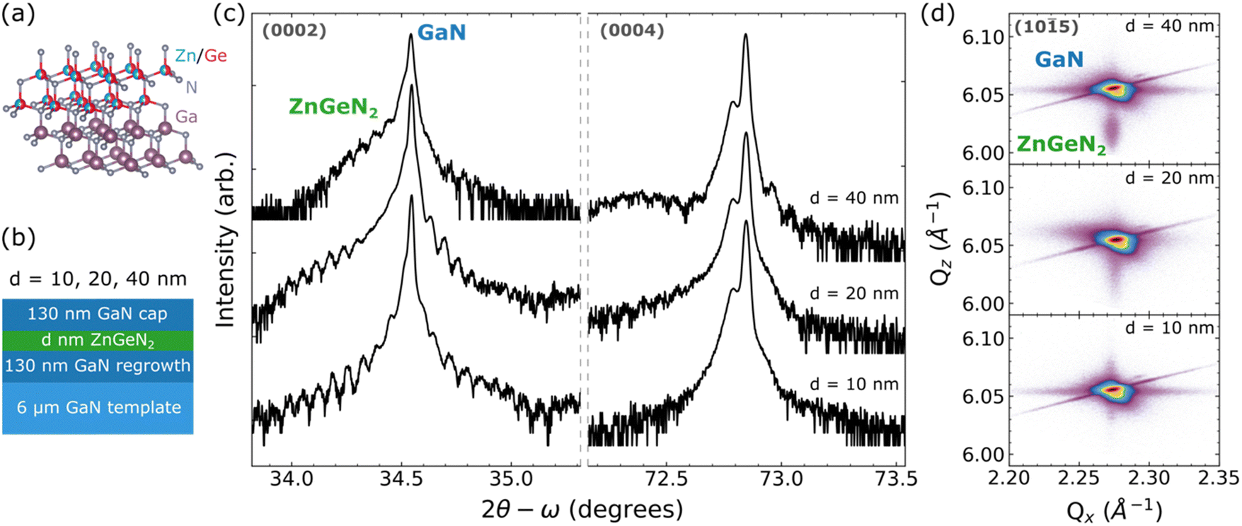 | ||
Fig. 1 (a) Crystal structure diagram of wurtzite GaN and cation-disordered ZnGeN2. (b) Layer diagram of the samples studied in this article consisting of a GaN regrowth, varied thickness (d nm) ZnGeN2 layer, and GaN cap. (c) High-resolution XRD symmetric scans of the (0002) and (0004) reflections taken in triple-axis geometry. (d) Asymmetric reciprocal space maps along the (10![[1 with combining macron]](https://www.rsc.org/images/entities/char_0031_0304.gif) 5) reflection to observe broadening mechanisms and strain. 5) reflection to observe broadening mechanisms and strain. | ||
Methods
GaN and ZnGeN2 were grown by molecular beam epitaxy (MBE) using previously published methods.20,22 In contrast to previous work on AlN substrates, GaN templates (6 μm thick, Si-doped, 3LCorp) were used as substrates. After loading and annealing, the GaN substrate was chemically cleaned with metallic gallium.15 N2 was supplied at 2.25 SCCM and activated at 500 W plasma power.21 ZnGeN2 was grown at 400–450 °C at a II/IV ratio ranging from 75![[thin space (1/6-em)]](https://www.rsc.org/images/entities/char_2009.gif) :1 to 250:1 using a Ge-limited growth flux of approximately 3 × 10⁻⁸ torr beam equivalent pressure (BEP). The III/V ratio for GaN was actively monitored with RHEED intensity transients.23 The substrate back-side thermocouple was calibrated to the melting point of Al using a pyrometer.
:1 to 250:1 using a Ge-limited growth flux of approximately 3 × 10⁻⁸ torr beam equivalent pressure (BEP). The III/V ratio for GaN was actively monitored with RHEED intensity transients.23 The substrate back-side thermocouple was calibrated to the melting point of Al using a pyrometer.
Structural quality was assessed by X-ray diffraction (XRD) and scanning transmission electron microscopy (STEM), chemical abruptness at interfaces and impurity analysis were assessed by X-ray energy-dispersive spectroscopy (EDS) and secondary ion mass spectrometry (SIMS). XRD was performed with a Panalytical MRD-Pro using Cu-kα radiation monochromated by a 4-bounce (400) Ge crystal and collimated by a Göbel mirror. The diffracted beam was limited to 12 arcsec by a 3-bounce Ge (220) monochromator (triple-axis geometry) for symmetric. A 255 × 255 pixel Si-CCD array was used to capture reciprocal space maps (RSMs) with a step size of 0.0025° 2θ. (Scanning) transmission electron microscopy studies were performed using a probe aberration corrected Titan Themis with SuperX EDS detector.
Optical properties were investigated by temperature- and power-dependent photoluminescence spectroscopy (PL). PL was excited with a 325 nm He–Cd laser with a spot size of approximately 100 μm at 0.01–1 mW power and recorded using a 0.3 m spectrometer coupled to a Si-CCD detector with a UV-sensitive coating. Despite the coating, the detector efficiency is <10% at wavelengths shorter than 400 nm, thus a white-light correction standard was applied. The laser line was filtered using a 325 nm razor-edge filter. For power-dependent data, PL signals were fit using a skewed Voigt function (from the built-in skewed Voigt model in the python lmfit module) to approximate the asymmetric line shape associated with the Fermi function and density of states to determine maximum intensity energy positions and peak amplitudes. Additional PL was performed using a 266 nm laser and a photomultiplier tube detector to rule out the presence of a cation-ordered ZnGeN2 band-to-band transition at higher energy.
Results and discussion
Structure and chemical properties
A series of GaN/ZnGeN2/GaN double heterojunctions were grown, varying the thickness of the ZnGeN2 layer (d = 10, 20, 40 nm, diagram in Fig. 1b) to determine the impact of ZnGeN2 thickness on interfacial, structural, and optical characteristics. GaN was regrown at 600 °C to a thickness of approximately 130 nm, after which the substrate temperature was lowered to 400 °C and the ZnGeN2 layer was grown under the same nitrogen plasma conditions used for GaN. Following the ZnGeN2 growth the substrate temperature was increased back to 600 °C at a ramp rate of 60 °C min−1, and GaN growth was initiated during the temperature ramp at 475 °C to prevent decomposition of the ZnGeN2 layer. The GaN cap was also approximately 130 nm thick. A control sample was grown without ZnGeN2 where the temperature was ramped to 400 °C after the regrowth and homoepitaxial GaN was initiated during the same temperature ramp at 475 °C to investigate the impact of low temperature GaN on XRD broadening. Symmetric XRD was measured around the (0002) and (0004) reflection, shown in Fig. 1c. We observe a broad diffraction peak associated with the thin ZnGeN2 layer as well as Pendellösung thickness fringes associated with the GaN cap. The thickness fringes were fit to a thickness of 130–135 nm, and the broad component associated with the ZnGeN2 layer corroborates the targeted thicknesses. The thickness fringes indicate the layers are uniform and the interfaces have low roughness.To observe the coherence of the ZnGeN2 epilayer, reciprocal space maps (RSMs) were performed around the (105) reflection in an asymmetric geometry (χ = 0°) (Fig. 1d). The streak tangential to the Ewald sphere at the reciprocal lattice point of GaN is an analyzer/detector streak arising from the width of the detector. The streak/point to the upper right of the main substrate peak is the sample streak artifact arising from slight variations in source wavelength, and the spread of the substrate peak extending down and to the right is the monochromator streak arising from the angular spread of the incident beam.24 Broadening of the GaN reciprocal lattice point is observed in Qx. The broadening in Qx is associated with a decrease of the lateral coherence length in the GaN cap,24 likely a result of dislocations generated at the GaN-on-ZnGeN2 top heterointerface. The in-plane broadening does not appear to increase as the ZnGeN2 film thickness is increased, indicating that these defects are not generated within the ZnGeN2 layer. An RSM of the control sample (Fig. S1, ESI†) does not show the broadening seen in the samples with a ZnGeN2 layer, supporting the hypothesis that these defects are generated at the interface between ZnGeN2 and GaN. The finite thickness of the GaN capping layer and ZnGeN2 layer produce crystal truncation rods, leading to broadening in Qz.
Mirroring the results for the symmetric scan, the ZnGeN2 epilayer is not distinguishable by diffraction in the 10 nm thick layer but becomes more distinct as the ZnGeN2 epilayer thickness increases. For the 40 nm sample the spot associated with ZnGeN2 is apparent at Qz ≈ 6.02 Å−1 and along the same in-plane Qx coordinate as GaN, indicating that the ZnGeN2 is psuedomorphic to GaN. The observed Qz value is slightly lower than expected for unstrained ZnGeN2 (6.03–6.04 Å−1), consistent with the observed in-plane compressive strain.
The 20 nm sample was investigated by transmission electron microscopy (TEM) to analyze structural and elemental uniformity using previously established methods.25,26Fig. 2 shows the overall microstructure of the epitaxially grown heterostructure. Some threading dislocations (black lines) were generated at the first ZnGeN2-on-GaN interface, and the majority are generated at the second GaN-on-ZnGeN2 interface. The inset is an aberration-corrected high-resolution high-angle annular-dark-field (HAADF) scanning transmission electron microscopy (STEM) image taken at [100] zone axis showing the ZnGeN2/MBE-GaN interface is well-defined and coherent. EDS elemental mapping, shown in Fig. 3, shows that both interfaces are uniform and fairly sharp. The EDS line scan in Fig. 3a demonstrates no significant variation between Zn and Ge within the ZnGeN2 layer, suggesting a stoichiometric film within the resolution of EDS, which cannot accurately quantify the nitrogen signal. The HAADF STEM image in Fig. 3b shows that the GaN cap immediately above the ZnGeN2, within a thickness of ∼20–30 nm, has a higher defect density than the remaining GaN cap. This defective layer is likely responsible for the broadening of the GaN reciprocal lattice point in Qx, which does not increase with increasing ZnGeN2 thickness, and is most likely correlated with the low temperature GaN nucleation.
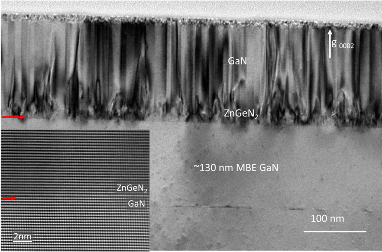 | ||
| Fig. 2 Microstructure of the 20 nm sample. Bright-field TEM image taken at the g = (0002) diffraction condition showing threading dislocations (black lines) generated at both ZnGeN2/GaN interfaces. Note that under this diffraction condition only threading dislocations with screw-components are visible. The inset is an aberration-corrected high-resolution high-angle annular-dark-field (HAADF) scanning transmission electron microscopy (STEM) image taken at the [100] zone axis showing the well-defined and coherent ZnGeN2/GaN interface. | ||
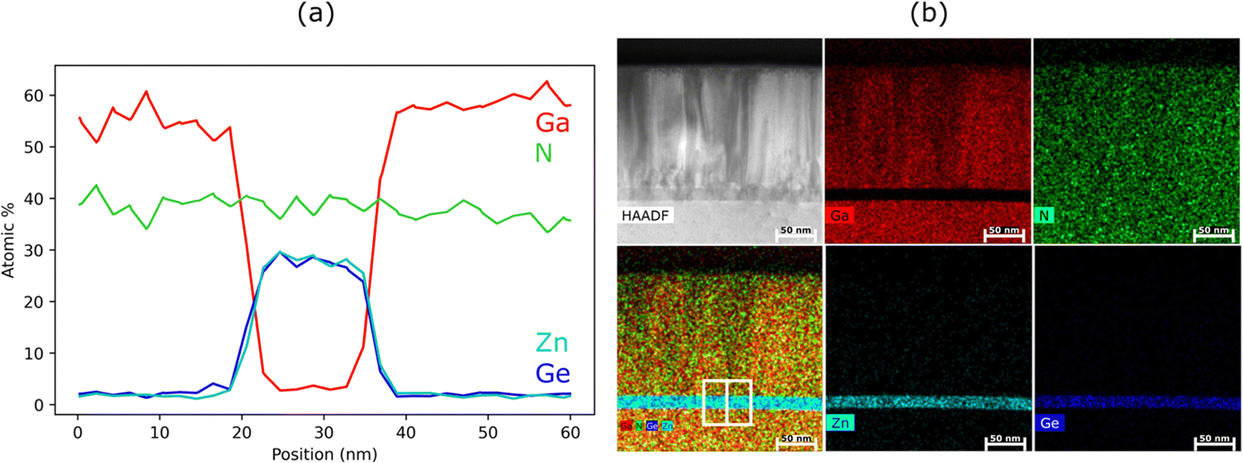 | ||
| Fig. 3 Compositional characterization of the 20 nm sample. (a) EDS line scan of the 20 nm sample (growth direction is left to right) shows the sample to have no significant variation between Zn and Ge within the ZnGeN2 layer, suggesting it is stoichiometric. (b) HAADF STEM image and corresponding X-ray energy dispersive spectroscopy elemental mapping shows the elemental distribution inside the film. The box in the 4-element overlay shows the approximate area of the EDS line scan shown in (a). | ||
Optical properties
PL was performed at room temperature (294 K) and at low temperature (4 K) and is shown in Fig. 4. There are three primary features in the spectra. From lower energy to higher energy at room temperature (Fig. 4a), there is the GaN yellow-band luminescence at 2.25 eV, a broad transition around 2.87–2.95 eV, and a band edge transition at 3.4 eV. We have previously determined that the broad transition at approximately 2.9 eV is associated ZnGeN2 by heteroepitaxial growth on AlN,13 however there is a competing signature of Zn-doped GaN at 2.88–2.89 eV.27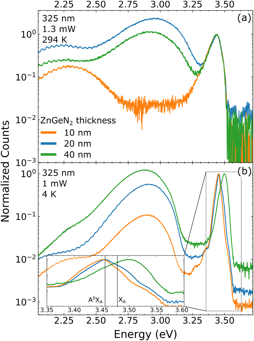 | ||
| Fig. 4 Room temperature (a) and low temperature (b) photoluminescence of the double heterojunctions with ZnGeN2 thicknesses of 10 nm, 20 nm, and 40 nm. PL is normalized to the GaN band edge signal, and raw counts per second data is shown in the ESI.† | ||
For the room-temperature spectra, the intensity of the GaN band-edge luminescence decreases as a function of increasing ZnGeN2 thickness (see the non-normalized data in Fig. S3, ESI†). As observed in the RSM's in Fig. 1d, the GaN cap does not become increasingly defective as a function of ZnGeN2 thickness, therefore the decreased intensity is consistent with absorption of band edge luminescence from the GaN substrate and buffer layer by the ZnGeN2 layer. The GaN yellow band luminescence is clear at approximately 2.25 eV with Fabry–Perot fringes characteristic of the template thickness. The peak associated with ZnGeN2 is located at 2.95 eV for the 20 nm ZnGeN2 layer and at 2.87 eV for the 40 nm ZnGeN2 layer but is not visible at room temperature for the 10 nm ZnGeN2 layer. The signature of Zn:GaN was reported as mostly invariant with temperature.27,28 The observed peak is broad, and not entirely uniform, therefore it is initially unclear if the signal includes both the near-band-edge electron to acceptor Zn:GaN transitions and the ZnGeN2 defect band.13,28
At low temperature (Fig. 4b) the band-edge peaks have sharpened and blue-shifted as expected. The intensity ratio of band-edge to broad-band luminescence follows a decaying trend consistent with increased attenuation of the GaN substrate and/or increased signal from the ZnGeN2 layer. We also observe two phonon-replicas in the 10 nm sample which decay in intensity as the ZnGeN2 layer is increased, also consistent with the absorption of substrate and/or buffer layer luminescence as the ZnGeN2 thickness is increased. The broad-band luminescence from the 10 nm sample peaks around 2.90 eV, consistent with previous reports for Zn:GaN. In addition, that signal is absent in the room-temperature measurement for the same sample, consistent with reports that Zn:GaN blue-band luminescence is quenched at room temperature.28 At low temperature the broad-band luminescence peak occurs at 2.91 eV for the 20 nm sample and 2.88 eV for the 40 nm sample, corresponding to a red-shift of approximately 400 meV at low temperatures for the 20 nm sample and a statistically insignificant blue-shift of 10 meV for the 40 nm sample. The red-shift with decreasing temperature is not consistent with band-edge luminescence, nor with Zn:GaN blue luminescence, therefore this signal is possibly correlated to defect-related luminescence in the ZnGeN2. It is likely that the peak consists of convolved signals from both Zn:GaN and ZnGeN2. Previous reports have correlated a broad set of signals in the range 1.7 eV to 2.2 eV with anti-site ZnGe–GeZn defect pairs, but we did not observe PL signal in this range.29
The highest-intensity peak energy for the 10 nm and 20 nm sample is found at 3.455 eV, consistent with the reported energy level of an acceptor-bound exciton (A0XA) in Zn:GaN.27 In addition, the energy position of the 1LO and 2LO phonon-replicas, 3.36 eV and 3.27 eV, is consistent with the reported positions of the phonon-replica of the A0XA for Zn:GaN.28 In contrast, we observe phonon replicas at 3.38 eV, 3.29 eV, and 3.2 eV in GaN templates that have not been grown on, consistent with the free-exciton bound phonon series (XA-LO) rather than the A0XA-LO series.28 This implies that the primary band-edge signal in the 10 nm and 20 nm samples originates from unintentionally Zn-doped GaN.
In contrast to the 10 nm and 20 nm samples, the highest-intensity peak energy for the 40 nm sample is found at 3.50 eV. The 10 nm and 20 nm samples also have higher-energy recombination signatures, visible in the inset of Fig. 4b, at approximately 3.48 eV and 3.52 eV. The 40 nm sample also shows a lower-energy shoulder around 3.45 eV which corresponds with the previously mentioned A0XA transition. The highest energy recombination in GaN occurs from the free-exciton series split by the valence bands (light and heavy hole plus split-off) at 3.478 eV, 3.484 eV, and 3.49 eV for XA, XB, and XC respectively.28 These signatures are difficult to observe, especially XB and XC. It is therefore unlikely that the recombination mechanism resulting in 3.50 eV emission is associated with free excitons in GaN. It is however possible that the first high-energy shoulder of the 10 nm and 20 nm samples corresponds to the XA transition in GaN, and it is unclear if this signature is also present in the 40 nm sample. We do not expect strain effects, which can alter the transition energy, to play a role in these results as there is no significant deviation from ideal lattice constants observed by reciprocal space mapping (Fig. 1).30,31 The other possibilities for emission at energies higher than the free exciton in GaN are band-edge emission from cation-ordered ZnGeN2 and Burstein–Moss shifted emission from degenerately n-type doped GaN. Low-temperature emission with a peak at 3.53 eV has been observed for degenerately doped GaN with Ge on the order of 3.5 × 1019 cm−3, however the associated room temperature band-edge signal is very broad with a peak at 3.46 eV.32 In contrast, we do not see an associated broad transition at room temperature with a higher-than-expected energy. To further investigate, a 20 nm ZnGeN2 sample was grown without a GaN cap (Fig. S4, ESI†). In this sample we still observe the A0XA, XA, and unexplained high energy signatures at 3.455 eV, 3.478 eV, and 3.55 eV respectively, but we do not observe the 3.50 eV transition indicating it is most likely due to degenerate Ge-doping in the GaN cap resulting from partial decomposition of the ZnGeN2 when increasing the substrate temperature for GaN growth. Decomposition would produce volatile Zn and N2, leaving behind excess Ge to incorporate in the GaN, consistent with defects observed in the first 30 nm of the GaN cap by HAADF STEM imaging.
To further understand the 2.9 eV transition, we have performed power-dependent measurements at low temperature (Fig. 5, raw data in Fig. S5, ESI†). 4K PL data was collected at 10 μW, 100 μW, and 1 mW to look for signatures of donor–acceptor pairs and bimolecular recombination.33 In Fig. 5 we observe a blue-shift in the broad 2.9 eV peak for the 10 nm sample, but not for the 20 nm or 40 nm sample. A blue-shift with increasing excitation intensity is a clear signature of donor–acceptor pair transitions due to a coulomb term between two localized states which is not present for other recombination mechanisms. This indicates that the recombination mechanism observed for the 10 nm sample is fundamentally different than the other samples. This is corroborated by the absence of room-temperature PL signal at 2.9 eV for only the 10 nm sample. Taken in context of the temperature-dependent PL where the 2.9 eV is absent at room temperature for the 10 nm sample only, we can conclude that the recombination signal in the 10 nm sample is indeed due to donor–acceptor pairs associated with Zn:GaN as previously reported.28 We can also conclude that ZnGeN2 is responsible for the defect signature observed in the 20 nm and 40 nm samples, and that the transition likely involves one free carrier (free-to-bound) as the signal does not blue-shift under increasing excitation power.33 A survey of ZnGeN2 defect calculation literature finds two possible origins for this free-to-bound signature at 2.9 eV. Native defect calculations suggest a GeZn antisite defect is the closest match with a (+2/0) charge transition level 2.9–3.1 eV above the valence band.34,35 Impurities from the GaN layer may also be contributing to the defect luminescence observed, and it is well-known that shuttered but hot sources in MBE may still contribute to background impurities. Impurity defect calculations predict the GaGe to be the most likely to form at 2.9 eV.36,37 Given that the ZnGeN2 layers are grown at a substrate temperature where Zn desorption is dominant and while the Ga cell is still hot but shuttered, we cannot rule out either candidate.
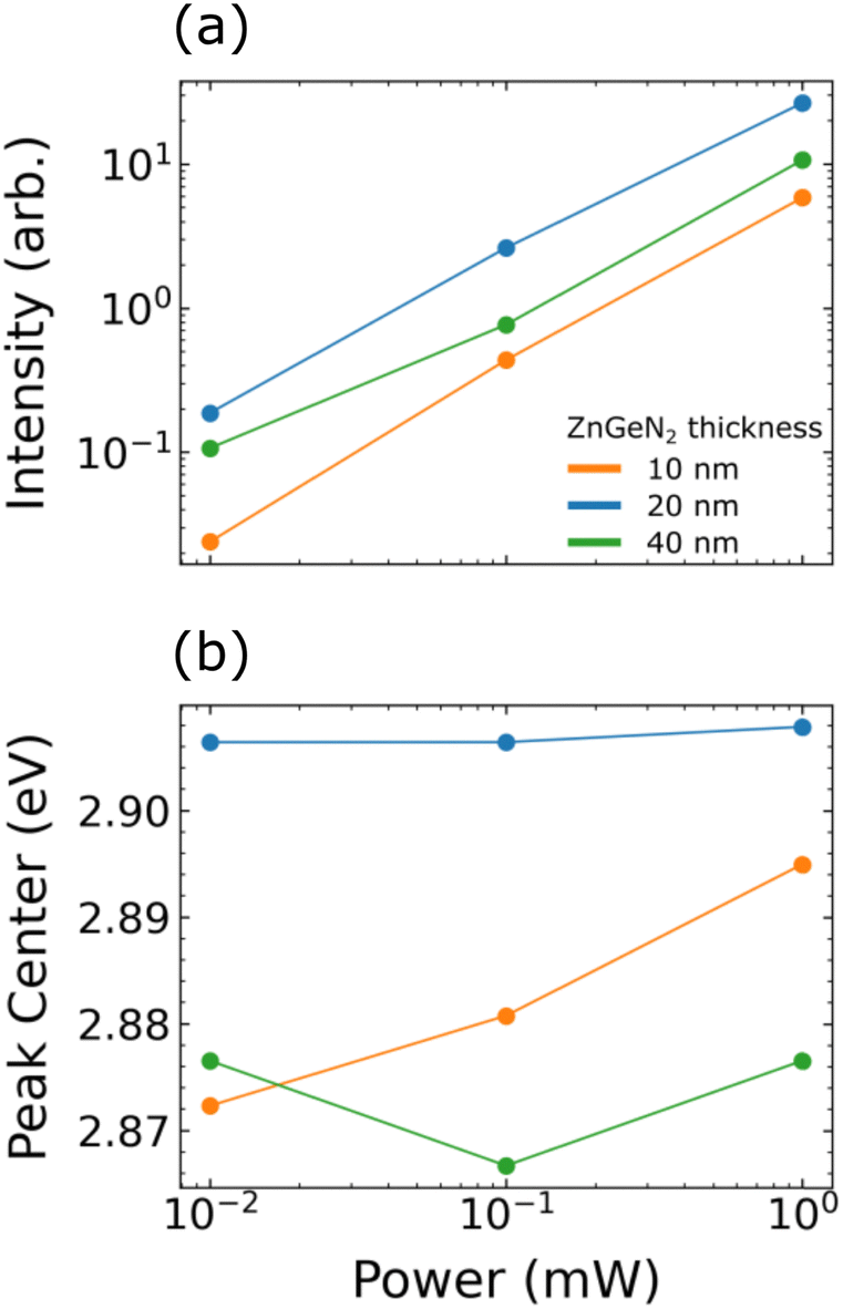 | ||
| Fig. 5 (a) Defect band peak intensity at low temperature as a function of excitation power. The three thickness show similar slopes, approximately 1 on a log–log scale, which is not indicative of a specific mechanism at the achievable excitation power range. PL peak center (b), also as a function of excitation power. Blue shifting is observed in the 10 nm sample, consistent with a donor-acceptor pair in Zn-doped GaN, while the 20 nm and 40 nm signal do not show any shift consistent with a free-to-bound transition. | ||
Conclusions
In conclusion, we have demonstrated coherent GaN/ZnGeN2/GaN double heterostructures grown by MBE. The structure was investigated by XRD and STEM, showing abrupt interfaces and psuedomorphic growth. RSMs confirmed the structural coherence but also showed a defective GaN cap independent of ZnGeN2 thickness, also confirmed by microscopy, suggesting defects are generated at ZnGeN2/GaN heterointerfaces. Threading dislocations nucleated at both interfaces were observed by STEM. PL showed a broad transition around 2.9 eV which consists of both an unintentionally Zn-doped GaN component and ZnGeN2 defect component. According to previously published intrinsic and extrinsic defect calculations this transition may be assigned to either a GeZn antisite defect or GaGe impurity. For thin ZnGeN2 layers, the recombination is primarily from unintentionally Zn-doped GaN as determined by temperature- and power-dependent measurements. For thicker ZnGeN2, the signal is a convolution of Zn-doped GaN and a free-to-bound defect transition in ZnGeN2. This work demonstrates that high-quality interfaces between ZnGeN2 and GaN are possible, however further study is required to reduce the threading dislocation density and unintentional Zn and Ge doping in GaN capping layers.Author contributions
M. B. Tellekamp synthesized the films, performed XRD characterization, wrote the manuscript, and helped conceive and supervise the project. M. K. Miller helped with data analysis and writing the manuscript. L. Zhou performed the STEM and EDS characterization and analysis. A. C. Tamboli helped conceived and supervise the project. All authors reviewed the manuscript.Data availability statement
The data that support the findings of this study are available from the corresponding author upon reasonable request.Conflicts of interest
There are no conflicts to declare.Acknowledgements
The authors would like to acknowledge Pat Dippo for acquiring the photoluminescence spectra, Matthew Brubaker for performing additional PL, the Steve Harvey for collecting SIMS data, and Jin-Su Oh for TEM sample preparation. This work was authored in part by the National Renewable Energy Laboratory, operated by Alliance for Sustainable Energy, LLC, for the U.S. Department of Energy (DOE) under Contract no. DE-AC36-08GO28308. Funding provided by the U.S. Department of Energy Office of Energy Efficiency Building Technologies Office. All electron microscopy and related work were performed using instruments in the Sensitive Instrument Facility at Ames National Lab. The Ames National Laboratory is operated for the U.S. Department of Energy by Iowa State University under Contract no. DE-AC02-07CH11358. The views expressed in the article do not necessarily represent the views of the DOE or the U.S. Government.References
- T. D. Moustakas, MRS Commun., 2016, 6, 247–269 CrossRef CAS.
- T. J. Flack, B. N. Pushpakaran and S. B. Bayne, J. Electron. Mater., 2016, 45, 2673–2682 CrossRef CAS.
- R. Sun, J. Lai, W. Chen and B. Zhang, IEEE Access, 2020, 8, 15529–15542 Search PubMed.
- T. Mukai, S. Nagahama, T. Kozaki, M. Sano, D. Morita, T. Yanamoto, M. Yamamoto, K. Akashi and S. Masui, Phys. Status Solidi A, 2004, 201, 2712–2716 CrossRef CAS.
- G. Meneghesso, G. Verzellesi, F. Danesin, F. Rampazzo, F. Zanon, A. Tazzoli, M. Meneghini and E. Zanoni, IEEE Trans. Device Mater. Reliab., 2008, 8, 332–343 CAS.
- D. Jena, J. Simon, A. (Kejia) Wang, Y. Cao, K. Goodman, J. Verma, S. Ganguly, G. Li, K. Karda, V. Protasenko, C. Lian, T. Kosel, P. Fay and H. Xing, Phys. Status Solidi A, 2011, 208, 1511–1516 CrossRef CAS.
- T. D. Moustakas, Phys. Status Solidi A, 2013, 210, 169–174 CrossRef CAS.
- I. Akasaki, Ann. Phys., 2015, 527, 311–326 CrossRef CAS.
- S. H. Sohel, A. Xie, E. Beam, H. Xue, J. A. Roussos, T. Razzak, S. Bajaj, Y. Cao, D. J. Meyer, W. Lu and S. Rajan, IEEE Electron Device Lett., 2018, 39, 1884–1887 CAS.
- Y. Zhang, M. Sun, J. Perozek, Z. Liu, A. Zubair, D. Piedra, N. Chowdhury, X. Gao, K. Shepard and T. Palacios, IEEE Electron Device Lett., 2019, 40, 75–78 Search PubMed.
- A. D. Martinez, A. N. Fioretti, E. S. Toberer and A. C. Tamboli, J. Mater. Chem. A, 2017, 5, 11418–11435 RSC.
- R. R. Schnepf, J. J. Cordell, M. B. Tellekamp, C. L. Melamed, A. L. Greenaway, A. Mis, G. L. Brennecka, S. Christensen, G. J. Tucker, E. S. Toberer, S. Lany and A. C. Tamboli, ACS Energy Lett., 2020, 5, 2027–2041 CrossRef CAS.
- M. B. Tellekamp, M. K. Miller, A. D. Rice and A. C. Tamboli, Cryst. Growth Des., 2022, 22, 1270–1275 CrossRef CAS.
- M. Rolles, B. Hyot and P. Miska, Phys. Status Solidi RRL, 2018, 12, 1800173 CrossRef.
- K. Du, C. Bekele, C. C. Hayman, J. C. Angus, P. Pirouz and K. Kash, J. Cryst. Grow., 2008, 310, 1057–1061 CrossRef CAS.
- C. L. Melamed, M. B. Tellekamp, J. S. Mangum, J. D. Perkins, P. Dippo, E. S. Toberer and A. C. Tamboli, Phys. Rev. Mater., 2019, 3, 051602 CrossRef CAS.
- J. J. Cordell, J. Pan, A. C. Tamboli, G. J. Tucker and S. Lany, Phys. Rev. Mater., 2021, 5, 024604 CrossRef CAS.
- M. R. Karim, B. H. D. Jayatunga, Z. Feng, K. Kash and H. Zhao, Cryst. Growth Des., 2019, 19, 4661–4666 CrossRef CAS.
- M. R. Karim, B. H. D. Jayatunga, M. Zhu, R. A. Lalk, O. Licata, B. Mazumder, J. Hwang, K. Kash and H. Zhao, AIP Adv., 2020, 10, 065302 CrossRef CAS.
- M. B. Tellekamp, C. L. Melamed, A. G. Norman and A. Tamboli, Cryst. Growth Des., 2020, 20, 1868–1875 CrossRef CAS.
- M. R. Karim, B. H. Dinushi Jayatunga, K. Zhang, M. Zhu, J. Hwang, K. Kash and H. Zhao, Cryst. Growth Des., 2022, 22, 131–139 CrossRef CAS.
- M. Moseley, D. Billingsley, W. Henderson, E. Trybus and W. A. Doolittle, J. Appl. Phys., 2009, 106, 014905 CrossRef.
- H. Ahmad, K. Motoki, E. A. Clinton, C. M. Matthews, Z. Engel and W. A. Doolittle, ACS Appl. Mater. Interfaces, 2020, 12, 37693–37712 CrossRef CAS PubMed.
- M. A. Moram and M. E. Vickers, Rep. Prog. Phys., 2009, 72, 036502 CrossRef.
- D. J. Smith, T. Aoki, J. Mardinly, L. Zhou and M. R. McCartney, Microscopy, 2013, 62, S65–S73 CrossRef PubMed.
- T. Ma, Z. Fan, B. Xu, T.-H. Kim, P. Lu, L. Bellaiche, M. J. Kramer, X. Tan and L. Zhou, Phys. Rev. Lett., 2019, 123, 217602 CrossRef CAS PubMed.
- M. R. H. Khan, N. Sawaki and I. Akasaki, Semicond. Sci. Technol., 1992, 7, 472 CrossRef CAS.
- M. A. Reshchikov and H. Morkoç, J. Appl. Phys., 2005, 97, 061301 CrossRef.
- M. S. Haseman, M. R. Karim, D. Ramdin, B. A. Noesges, E. Feinberg, B. H. D. Jayatunga, W. R. L. Lambrecht, M. Zhu, J. Hwang, K. Kash, H. Zhao and L. J. Brillson, J. Appl. Phys., 2020, 127, 135703 CrossRef CAS.
- N. L. Adamski, D. Wickramaratne and C. G. Van de Walle, J. Mater. Chem. C, 2020, 8, 7890–7898 RSC.
- Q. Yan, P. Rinke, A. Janotti, M. Scheffler and C. G. Van de Walle, Phys. Rev. B: Condens. Matter Mater. Phys., 2014, 90, 125118 CrossRef.
- M. Feneberg, S. Osterburg, K. Lange, C. Lidig, B. Garke, R. Goldhahn, E. Richter, C. Netzel, M. D. Neumann, N. Esser, S. Fritze, H. Witte, J. Bläsing, A. Dadgar and A. Krost, Phys. Rev. B: Condens. Matter Mater. Phys., 2014, 90, 075203 CrossRef CAS.
- I. Pelant and J. Valenta, Luminescence Spectroscopy of Semiconductors, Oxford University Press, 2012 Search PubMed.
- C. L. Melamed, J. Pan, A. Mis, K. Heinselman, R. R. Schnepf, R. Woods-Robinson, J. J. Cordell, S. Lany, E. S. Toberer and A. C. Tamboli, J. Mater. Chem. C, 2020, 8, 8736–8746 RSC.
- N. L. Adamski, Z. Zhu, D. Wickramaratne and C. G. Van de Walle, J. Appl. Phys., 2017, 122, 195701 CrossRef.
- N. L. Adamski, Z. Zhu, D. Wickramaratne and C. G. Van de Walle, Appl. Phys. Lett., 2019, 114, 032101 CrossRef.
- D. Skachkov and W. R. L. Lambrecht, J. Appl. Phys., 2020, 127, 075707 CrossRef CAS.
Footnote |
| † Electronic supplementary information (ESI) available. See DOI: https://doi.org/10.1039/d3tc02425c |
| This journal is © The Royal Society of Chemistry 2023 |