DOI:
10.1039/D3TC01990J
(Paper)
J. Mater. Chem. C, 2023,
11, 13981-13990
Gate-tunable rectification and photoresponse in a MoTe2/SnS2 van der Waals heterostructure based P–N diode†
Received
8th June 2023
, Accepted 22nd September 2023
First published on 22nd September 2023
Abstract
The p–n junction, one of the prominent electrical components capable of being utilized in electronics and optoelectronics, has attracted renewed interest due to recent research in two-dimensional (2D) materials. In this work, we constructed a heterostructure p–n diode based on MoTe2 and SnS2. Sweeping the back-gate voltage (Vbg) effectively results in a high rectification ratio of 2.79 × 10⁵ at Vbg = +10 V and the lowest ideality factor (η) of about 1.25 was achievedwhen Vbg = −30 V. The interlayer electron–hole recombination is responsible for the variation in rectification behavior. This photodiode exhibits effective photodetection capabilities and promising merit statistics. The maximum change in photocurrent (Iph) is measured to be about 90 nA at Vds = 0.9 V, and the device exhibited a high responsivity (R) of 5.8 × 10⁴ mA W−1, while the maximum external quantum efficiency (EQE) and detectivity are calculated to be about 3.27 × 10⁴ (%) and 2.47 × 10¹⁰ Jones for the device, respectively, when illuminated with 220 nm wavelength incident light at a power intensity of 11 mW cm−2. The average rise/fall times for the 220 nm wavelength at Vds = 0.9 V are observed to be 0.29 s/0.38 s, respectively. We examined the photoresponse of the device as a function of time at different wavelengths (λ = 970–220 nm) of the incident light and at different power intensities (P = 11–44 mW cm−2) of the incident light. The maximum values of Voc = 0.32 V and Isc = −0.40 nA were achieved at P = 44 mW cm−2. The p-MoTe2/n-SnS2-based device has excellent rectifying and optoelectronic properties.
Introduction
Two-dimensional (2D) layered materials are considered to have outstanding potential in electronics and optoelectronics due to their desirable physical characteristics.1,2 Because of their customized energy band alignments and ultrathin structural characteristics, van der Waals (vdW) heterojunctions established on thin 2D materials have ushered in a new era for next-generation optoelectronics.3 Graphene has received a great deal of attention in the fields of spintronics,4–6 electronics,7 and optoelectronics.7,8 In another class, depending on the layer thickness, 2D transition metal dichalcogenide (TMDC) materials have band gaps between 1 eV and 2.5 eV. A broad range of applications, including photodetectors,9,10 field-effect transistors,11,12 flexible devices,13 logic circuits,14 and optical communication,15,16 are possible due to the band gap variation between the multilayer indirect gap and the monolayer direct gap.17,18 Ever more research has focused on p–n junctions made of various 2D layered materials, creating a new material platform for investigating novel physical features and new device applications.19–21 One may tune the energy band alignment by joining individual layers of different 2D layered materials for the vdW heterostructure with a sharp junction at the atomic scale. This provides a wealth of options for investigating the fundamentals of new electrical and optical features. Thus, TMDCs/TMDCs or TMDCs/graphene heterostructures have been the focus of current studies in the field of 2D TMDCs.22,23 In addition, due to their ultrathin nature and steep interfacial charge-carrier gradient, 2D vdW heterostructures have significant tunability in band alignment and carrier density, providing an alternative avenue for versatile electrical and optoelectronic applications. For example, in atomically thin GaTe/MoS2 and WSe2/MoS2 p–n heterojunctions, the external quantum efficiency (EQE) of 40–60% is attained.23,24 In addition, photodetectors based on MoTe2/MoS2 vdW heterojunctions are also demonstrated,25,26 and gate-tunable photovoltaic behavior is also seen in WSe2/MoS2 heterojunctions.27 Gate tunable rectification and photoresponse of the heterostructure GeSe/WS2 based p–n diode were also observed.28 Yet, due to the limited photocurrent flow without an external bias control, the responsivity of such devices remains low. As a result, greater efforts are required to increase the effectiveness of photodetectors based on TMDCs for future nanoscale optoelectronic devices. Molybdenum ditelluride (MoTe2) has played a significant role in electronic devices. MoTe2 exhibits a direct band gap that ranges from 0.9 to 1.1 eV, depending on the material's thickness and lattice structure.29 MoTe2 has potential use in a variety of devices, including digital logic circuits,30 solar cells,31 and chemical sensors32 owing to its effective mobility and lack of dangling bonds. SnS2 offers intriguing opportunities for creating heterostructures with other 2D materials with various crystallographic structures. A band gap of 2.28 eV is thus found that corresponds to the band gap of SnS2.33 SnS2 has been identified as an n-type semiconductor because of its technological significance for next-generation electronic/photonic applications. Thus, layered two-dimensional (2D) SnS2 has garnered significant interest.34,35
Here, we present a heterostructure p–n diode consisting of MoTe2 and SnS2. Sweeping the back-gate voltage effectively results in a high rectification ratio of 2.79 × 10⁵. The variance in rectification behavior is caused by interlayer electron–hole recombination. Effective photodetection and inspiring merit statistics characterize this photodiode. The maximum change in photocurrent (Iph) is measured to be about 90 nA. The device exhibited a high responsivity (R) of 5.8 × 10⁴ mA W−1, while the maximum external quantum efficiency (EQE) and detectivity (D*) are calculated to be about 3.27 × 10⁴ (%) and 2.47 × 10¹⁰ Jones for the device when illuminated with incident light at a wavelength (λ) of 220 nm and a Vds of 0.9 V, respectively. Furthermore, the photoresponse of the device was investigated under the illumination of light of various wavelengths and at different power intensities of incident light. The p-MoTe2/n-SnS2-based device exhibits remarkable optoelectronic and rectifying characteristics.
Device fabrication and characterization
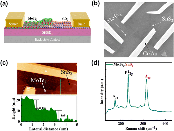
Thin layers of MoTe2 and SnS2 were formed using the mechanical exfoliation method. Using an adhesive tape, flakes of both materials were mechanically exfoliated. These were then captured by a polydimethylsiloxane (PDMS) stamp on a glass slide as part of the transfer procedure. By positioning the PDMS stamp on a Si/SiO2 substrate and peeling it off, few layers of SnS2 and then MoTe2 are transferred to the target substrate using the dry transfer method. A micro-aligner stage was used to carefully manage the transfer of each flake, which was monitored by a CCD camera. Then the substrate containing these layers (heterojunction) was dipped into acetone/methanol for 2 hours for the removal of residues. After this, the substrate was dried using nitrogen (N2) gas. Polymethylmethacrylate (PMMA) was coated on the substrate that contains the heterostructure of MoTe2–SnS2, and contact electrode patterns were formed by e-beam lithography on the layer. Then the contact electrodes composed of Cr/Au (5 nm/60 nm) were deposited using a thermal evaporator. Then, the substrate was placed in acetone/methanol for the removal of unwanted metals, after this the substrate was dried using nitrogen gas. Finally, we connected the gate at the back (Vbg: back gate) of the Si/SiO2 substrate with indium wire. The schematic of the device that contains the heterostructure of MoTe2–SnS2 is illustrated in Fig. 1(a). The scanning electron microscopy (SEM) image of the MoTe2–SnS2-based device is presented in Fig. 1(b). An atomic force microscope (AFM: Nano Focus) is employed to verify the thickness of the heterostructure. Fig. 1(c) depicts the AFM image of the device and thickness of the heterostructure of MoTe2–SnS2. The Renishaw spectrometer with a 514 nm excitation wavelength is utilized to check the Raman spectra. The Raman peak shows the basic characteristics of the MoTe2–SnS2 heterojunction as shown in Fig. 1(d). Two peaks can be seen in the Raman spectra of MoTe2 at 172.4 cm−1 and 232.9 cm−1, respectively. These peaks correspond to the out-of-plane vibrational mode A1g and the in-plane vibrational mode E12g, and the A1g mode at 315.7 cm−1 corresponds to SnS2. The individual Raman spectra of both MoTe2 and SnS2 are presented in Fig. S1(a and b) (ESI†). For SnS2, in the heterojunction region, the peak got contribution of both materials, representing the presence of two different materials. Specifically, a reduction in the peak intensity for SnS2 due to screening from MoTe2 is clearly observed. In addition, we have observed a minor blue shift for the peak corresponding to A1g, this may be due to the transfer of holes from MoTe2 to SnS2 material, and a minor blue shift is also seen in the peaks of MoTe2 after stacking with SnS2.
 |
| | Fig. 1 (a) Schematic illustration of the p–n device. (b) SEM image of the p–n heterostructure MoTe2–SnS2-based device; the scale bar is 5 μm. (c) AFM profile of the heterostructure. (d) Raman spectra of the MoTe2–SnS2 heterostructure. | |
We created intensity maps to visualize their spatial distribution across the heterostructure. These maps represent the variation in Raman intensity at specific Raman shift values and provide insights into the distribution and interaction of the materials within the heterostructure. We have observed the Raman intensity of MoTe2/SnS2, which shows that the MoTe2 and SnS2 grains are laterally and flawlessly spliced in the heterostructure without the construction of alloy phases at their junction. The area selected for Raman mapping investigated is highlighted in Fig. 2(a). Graphical depiction of the Raman intensity mapping obtained at 172.43 (A1g), and 232.93 cm−1 (E12g) for MoTe2, and 315.78 cm−1 (A1g) for SnS2 is shown in Fig. 2(b–d). The Raman mapping data show the perfect formation of the vdW heterostructure based on MoTe2–SnS2.
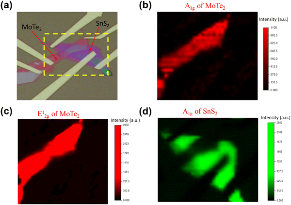 |
| | Fig. 2 (a) Optical image of the device that shows the area selected for Raman mapping. (b) Raman intensity maps of A1g of MoTe2. (c) Raman intensity maps of E12g of MoTe2. (d) Raman intensity maps of A1g of SnS2. Graphical representation of Raman intensity mapping at 172.43 and 232.93 cm−1 for MoTe2, and 315.78 cm−1 for SnS2. | |
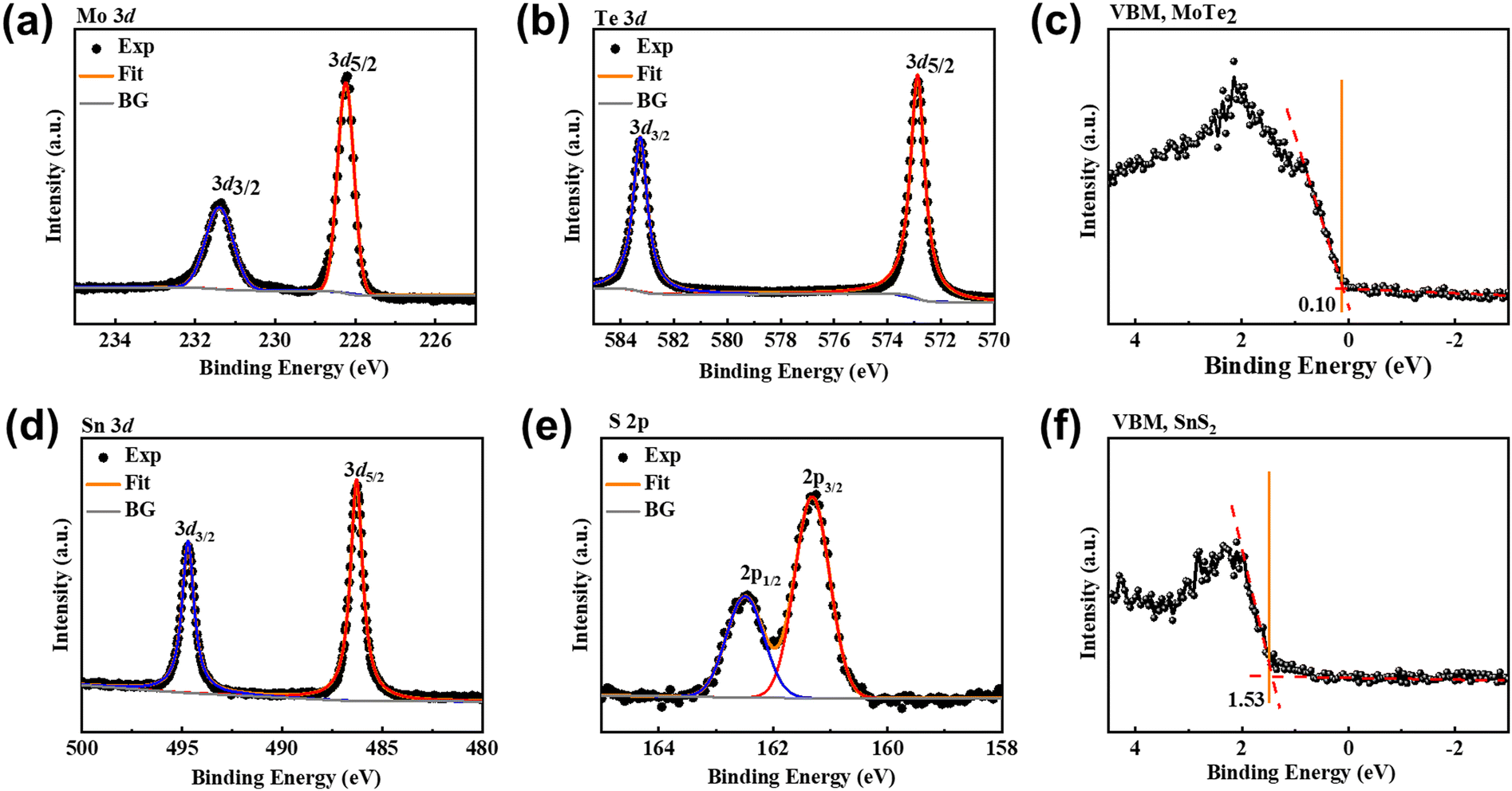
The materials MoTe2 and SnS2 were characterized by X-ray photoelectron spectroscopy (XPS). We have utilized an XPS (PHI 5000 Versa Probe III, ULVAC PHL, Japan), with a monochromatic Al Kα (1486.6 eV) X-ray source with a beam spot size of ∼20 μm. Fig. 3(a and b) shows the XPS spectra of Mo and Te, and the fitted peaks for the MoTe2 flake are consistent with the previously reported results.36 The corresponding valence band maximum (VBM) spectra of MoTe2 are presented in Fig. 3(c) and are valued at ∼0.10 eV. Fig. 3(d and e) shows the XPS spectra of Sn3d5/2, Sn3d3/2, S2p3/2 and S2p1/2. The VBM spectra of SnS2 are depicted in Fig. 3(f), which correspond to the value of ∼1.53 eV. The fitted Sn and S2 binding energies of SnS2 are in good agreement with the previous report.37 The XPS peaks are well defined and show that the flakes of MoTe2 and SnS2 are of high quality with no detectable oxidation state present on the surface of flakes. The separation between Mo3d3/2 and VBMMoTe2 and Sn3d5/2 and VBMSnS2 is illustrated in Fig. S2(a) (ESI†). Based on the XPS data, we have approximately calculated the band alignment of MoTe2–SnS2-based sample. The valence band offset is observed to be ≈1.43 eV, and the detailed calculation is shown in the ESI.† Based on valence band offset (VBO) approximate data obtained through XPS, we have calculated the conduction band offset (CBO) of 0.25 eV for MoT2–SnS2 and illustrated the band alignment. The detailed calculation is shown in Fig. S2(a and b) (ESI†).
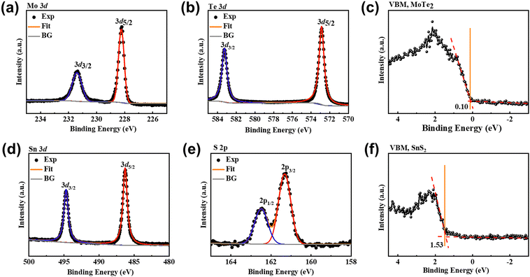 |
| | Fig. 3 XPS spectra: (a) Mo 3d peaks. (b) Te 3d peaks. (c) VBM of MoTe2. (d) Sn 3d peaks. (e) S 2p peaks. (f) VBM of SnS2. | |
Results and discussion
Electrical and photoresponse investigation
The IV curves were obtained at various back gate voltages (Vbg) using a Keithley 2400 (source meter) and a picometer (Keithley 6485) to assess the drain current. The photoresponsivity and EQE were evaluated using a light source of various wavelengths and irradiation power of different intensities. All measurements were taken at room temperature, to allow light illumination of the whole sample, and the device was placed inside a closed glass box under a high vacuum.
Electrical transport and rectification effects in MoTe2/SnS2 p–n diodes
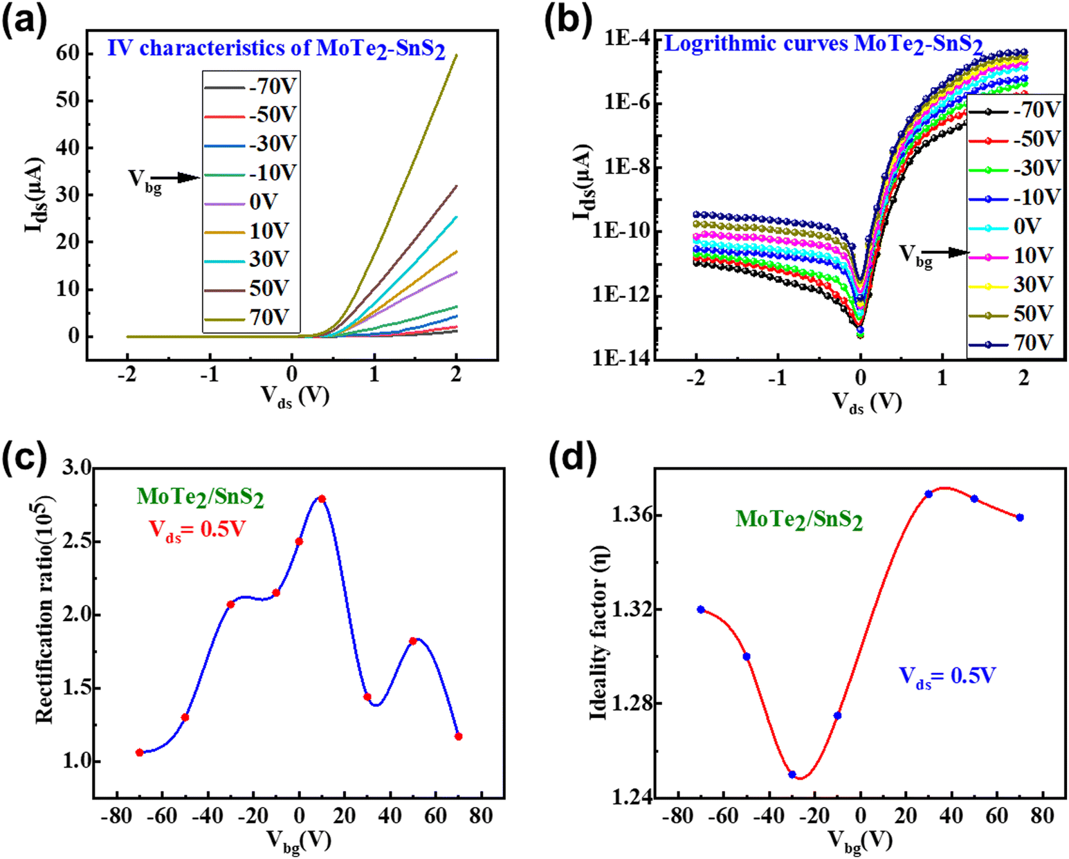
The electrical characteristics of both materials were examined individually also, and the I–V curves of separate MoTe2 and SnS2 at various back gate voltages are exhibited in Fig. S3(a and b) (ESI†). Each MoTe2 and SnS2 transfer curve exhibits obvious p- and n-type characteristics, respectively, as presented in Fig. S3(c and d) (ESI†). The source electrode was linked to MoTe2 (p-type) in our measurement approach, whereas drain contact was linked with SnS2 as indicated in Fig. 1(b). The I–V characteristics curves in linear scale for the MoTe2–SnS2 heterostructure at various back gate voltages are illustrated in Fig. 4(a), where the source–drain voltage range is −2 V to +2 V. The IV relation employed for typical p–n diodes made of semiconductors may be utilized to investigate the output properties of vdW's heterojunction-based p–n devices.38 The following equation provides the value for the current “I” via the diode:| | 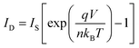 | (1) |
where Is refers to the saturation current, k is the Boltzmann constant, η refers to the ideality factor and q is the electronic charge. The I–V curves of the p–n diodes are presented in logarithmic scale as shown in Fig. 4(b). We define the rectification ratio (R.R = If/Ir) as the fraction of the forward current (If) and reverse-bias current (Ir) in order to test the rectification effect. We have attained a high rectification ratio of 2.79 × 10⁵ at back gate voltage Vbg= +10 V during the back-gate sweep effectively. Since Ir reduces more successfully in the negative Vbg than in the previously reported BP/MoS2 configuration, the R.R value is increased further three times.39,40 The high rectification rate is ascribed to two causes. The larger barrier height for Vbg < 0 V is the first explanation for the reduced reverse-bias leakage current. Expectedly, the barrier height between MoTe2 and SnS2 decreases for the positive Vbg, which in turn brings down the depletion width. Similar to this, a negative Vbg raises the barrier height and widens the depletion breadth. The tuning of the Schottky barrier (SB) height through gate-voltage at the metal/TMDC contact is the additional factor that causes the enhancement of the rectification ratio. The variation in the rectification ratio of the device at various gate voltages is illustrated in Fig. 4(c). Vbg has a significant impact on the MoTe2/SnS2 heterojunction p–n diode's output characteristics. The ideality factor at different back gate voltages is calculated; the variation in the ideality factor at various gate voltages is represented in Fig. 4(d). The detailed calculation for the ideality factor is expressed in the ESI† (Fig. S4). The lowest value of ideality is 1.25, which is achieved at Vbg = −30 V.
 |
| | Fig. 4 (a) Ids–Vds characteristic curves of the MoTe2–SnS2 heterostructure at various back gate voltages (Vbg); the linear scale. (b) Logarithmic scale. The maximum rectification ratio is 2.79 × 10⁵ mA W−1. (c) The change in the rectification ratio of the device at various back gate voltages. (d) The variation in the ideality factor at different gate voltages. | |
Fig. 5(a) demonstrates the energy-band diagram in p-MoTe2 and n-SnS2 with work functions, conduction band (CB) minima, and valence band (VB) maxima. In the case of SnS2, the Fermi level is close to the CB, which displays n-type behavior, while the Fermi level of MoTe2 is close to the VB, which displays p-type behavior. The band diagram of the MoTe2/SnS2 vdW heterostructure at zero Vbg is shown in Fig. 5(b) along with the associated Fermi level. The second part depicts a zoomed-in picture of the band configuration following the contact with zero Vbg. The Fermi level may be manipulated using the gate voltage, which modulates the charge carrier densities (holes and electrons) in p-MoTe2 and n-SnS2, correspondingly, and hence the rectification ratio as well. The Fermi level shifts away from the “CB” at Vbg < 0 V, increasing the potential barrier at the junction of the MoTe2/SnS2 vdW heterostructure diode, which generates a strong rectifying current. When Vbg > 0 V, the Fermi level moves toward the CB, lowering the barrier height. The manipulation of charge carriers (holes and electrons) and band positions of the MoTe2/SnS2-based diode by gate voltage offers an alternative way to fabricate very competent vdW heterojunctions.
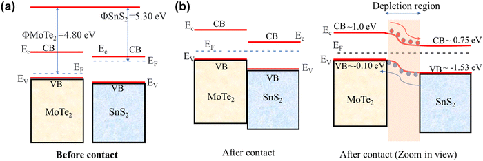 |
| | Fig. 5 Schematic illustration of the band diagram for the p-MoTe2/n-SnS2 structure-based diode at Vbg = 0 V. (a) Schematic signifies the band diagram of a p-MoTe2/n-SnS2 diode before connection, and (b) symbolizes the diode after connection. | |
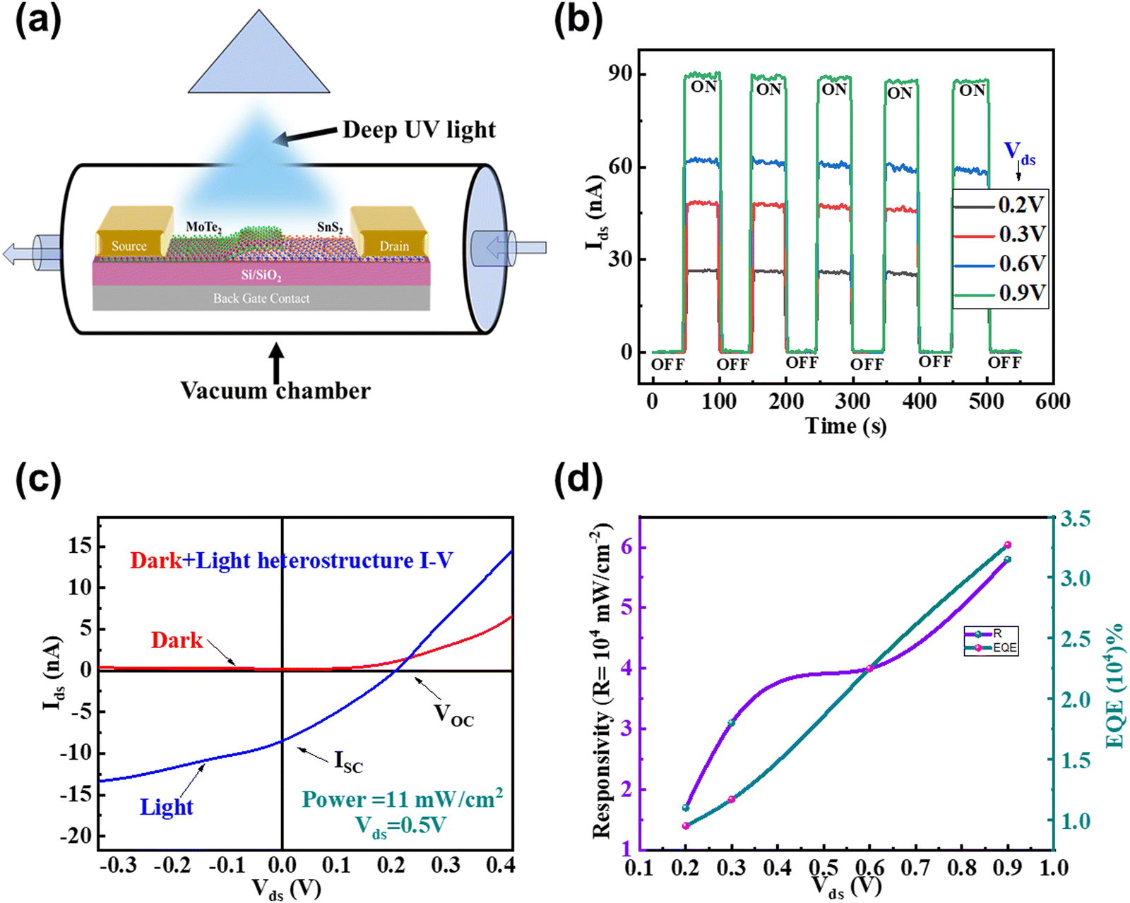
Optoelectronic properties of MoTe2/SnS2 p–n diodes
The optoelectronic properties of devices made of 2D materials have been the focus of ongoing research. Because the charge transfer differs from that of common p–n diodes, we studied the photoresponse to further investigate the potential exciting optoelectrical performance. The p-MoTe2/n-SnS2 heterojunction has high photovoltaic capabilities in addition to good electric qualities. The schematic of the photocurrent measurement approach is illustrated in Fig. 6(a), where the device is placed in a glass vacuum chamber. DUV light was beamed on the diode, causing a significant number of electron–hole pairs to form in both the SnS2 and MoTe2 layers. These photoinduced charge carriers penetrate the barrier, producing a strong photoresponse. The individual photocurrents of the 2D layers MoTe2 and SnS2 at different gate voltages are presented in Fig. S5 and S6 (ESI†), respectively. The MoTe2/SnS2 p–n diode is lit by light with the wavelength (λ) of 220 nm and an irradiation power (P) of 11 mW cm−2. The photocurrent of the device at various source–drain voltages (Vds) based on the MoTe2–SnS2 heterostructure is shown in Fig. 6(b). This illustrates how the photocurrent changes as a light is turned on and off repeatedly. A probable photo-switching mechanism is suggested by the photocurrent's on-and-off switching behavior. The maximum change in photocurrent (Iph) is found to be about 90 nA at Vds = 0.9V. Due to a rise in the built-in potential and charge carrier, we saw that the value of photocurrent rose at higher voltages. The large photovoltaic behavior is caused mostly by type-II band arrangement and a greater built-in potential at the junction, which efficiently distinguishes the photo-excited electron–hole pairs. The device exhibited a high responsivity (R) of 5.8 × 10⁴ mA W−1 at Vds = 0.9 V. The following formula is used to derive the photoresponsivity (R).| |  | (2) |
where P is the incident light power, A is the effective area (14 μm2) and Iph is the photocurrent. The detectivity D* = RA1/2/(2e.Idark)1/2 is also calculated, where R denotes responsivity, “A” is the effective area, e is the charge of the electron, and Idark is the dark current,41,42 and the detectivity (D*) is about 2.47 × 10¹⁰ Jones. The electrons and holes collected in the n-SnS2 and p-MoTe2 layers, respectively, result in the development of an open-circuit voltage (VOC). These retrieved electrons and holes in SnS2 and MoTe2 quickly recombine through an external circuit, producing a short-circuit current (ISC). At room temperature, our device represented an open circuit voltage (Voc) of 0.20 V and a short circuit current (Isc) of −8.5 nA and when Vg = 0 as presented in Fig. 6(c). This is due to the high photo-absorption and effective photoinduced electron–hole pair production. The amount of photo-generated carriers per incident photon per second is defined as the EQE, and the following equation was used to obtain the EQE,43,44| |  | (3) |
where ‘h’ refers to Plank's constant, c denotes the speed of light, e is the electron charge (e), and λ is the wavelength of light. The EQE value is determined from light absorption and the buildup of photo-generated carriers. In comparison to all previously reported p–n heterojunctions, we achieved the greatest EQE (%) of 3.27 × 10⁴% at Vds = 0.9 V, along with improved responsivity and other electronic/optoelectronic characteristics.45–47 The change in “R” and “EQE” at different Vds is depicted in Fig. 6(d). Moreover, because of the significant built-in potential, a quick photo-carrier separation and the associated short transit time may lead to a significant gain and a significant EQE.48,49Fig. 6(b and c) indicate that the rise in the forward- and reverse-bias currents is related to the creation of electron–hole pairs brought on by illumination. When illuminated, the charges are separated at the junction,50,51 causing the electrons to collect on the top face of the SnS2 and the holes to belong to the bottom face of MoTe2. Due to the formation of dipoles in the junction region, increased electron–hole pair production is subsequently induced.52 Our MoTe2/SnS2 heterojunctions were shown to have a significant promise for both electrical and optoelectronic devices due to their effective photoresponsivity and high EQE. Another cause for the high EQE is the built-in voltage at the interface.24,53 Due to the slight difference among “CB” maximums of MoTe2 and SnS2, electrons and holes recombine in greater quantities at the junction between MoTe2 and SnS2, increasing the built-in potential. Furthermore, it is envisaged that the screening against coulomb impurities would be improved in the devices based on 2D materials, resulting in a larger EQE.24 The average rise/fall time is 0.29 s/0.38 seen for the wavelength of 220 nm at Vds = 0.9 V, respectively. The fitting/calculation details related to rise/fall time is shown in tabular and graphical form in Fig. S7(a and b) (ESI†).
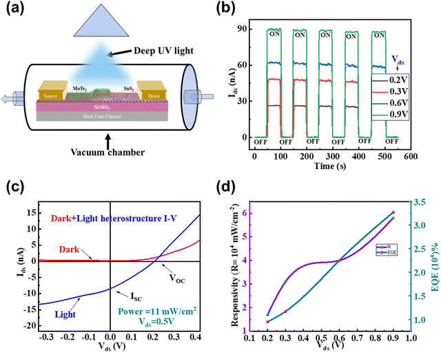 |
| | Fig. 6 (a) Schematic of the p–n device for photodetection. (b) Photocurrent at Vg = 0, for Vds= 0.2–0.9 V with incident light (λ = 220 nm) and power intensity 11 mA cm−2. (c) I–V curves in the dark and under light, representing ISC = −8.5 nA and Voc = 0.20 V at Vg = 0. (d) The change in responsivity at different values of Vds. (e) The enhancement in the EQE at different values of Vds. | |
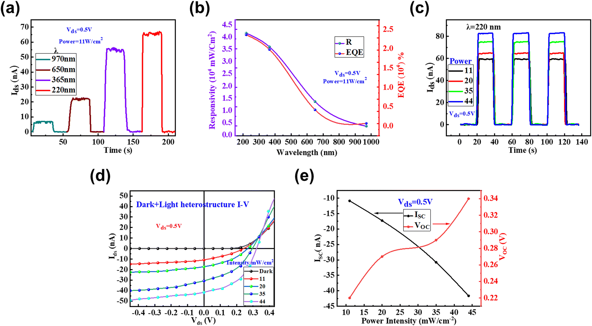
We have examined the photoresponse of the device as a function of time at different wavelengths (λ = 970, 650, 365 and 220 nm) of the incident light at Vds = 0.5 V as shown in Fig. 7(a). The photocurrent of the device is enhanced as the wavelength of incident light is decreased. The observed photocurrent rises as the wavelength decreases, reaching its maximum value at λ = 220 nm because of the higher production of electron–hole pairs at low wavelengths. Because there are more excited charge carriers, smaller wavelengths produce greater photocurrent and responsivity values. This behavior is related to strong absorption and high photon energies at low wavelengths, which is compatible with the findings of earlier research.54 We have calculated the responsivity (R) and external quantum efficiency (EQE) at various wavelengths of incident light. The values of R and EQE decreased as the wavelength of incident light was enhanced as shown in Fig. 7(b). Photoresponse of the device based on the MoTe2/SnS2 heterostructure was investigated as a function of time at different power intensities (P = 11, 20, 35, 44 mW cm−2) of the incident light at a wavelength λ = 220 nm for Vds = 0.5 V shown in Fig. 7(c). We have seen that the photocurrent is enhanced as the power of radiant light is raised. Fig. 7(d) shows the IV curves under dark and incident light of different power intensity, and we can observe the change in Voc and Isc. It is observed that as the incident light's intensity increases, the reverse current rises steadily under the light. This is due to greater electron–hole pairs being generated at the p-MoTe2/n-SnS2 junction because of the incoming light, increasing the reverse and forward currents. Furthermore, Voc is non-linear and the value of Isc is linearly reliant on the intensity of the laser light as shown in Fig. 7(e). The maximum values of Voc = 0.32 V and Isc = −0.40 nA were achieved at P = 44 mW cm−2. Furthermore, we added the Table 1 that summarizes the various characteristics of different photodetectors based on various 2D materials. The p-MoTe2/n-SnS2-based device exhibits remarkable optoelectronic and rectifying characteristics.
 |
| | Fig. 7 (a) Photocurrent of the device based on the MoTe2/SnS2 heterostructure as a function of time at different wavelengths of incident light. (b) Change in R and EQE as a function of wavelength, which shows a decreasing trend. (c) Photoresponse of the device at different power intensities of incident light at the wavelength of 220 nm. (d) I–V characteristics curve of the device under the dark and with the radiant light of different power intensities. (e) Variation in VOC and ISC under different power intensities of radiant light (P = 11, 20, 35, 44 mW cm−2). | |
Table 1 The summary of photodetectors based on various 2D materials
| Materials |
Wavelength (λ) |
Responsivity |
Detectivity (D*) Jones |
EQE (%) |
Ref. |
| GaSe/PtSe2 |
520 nm |
1.78 A W−1 |
3.5 × 10¹² |
405 |
55
|
| WSe2/ReS2 |
600 nm |
3 A W−1 |
8.39 × 10¹⁰ |
600 |
56
|
| BP/MoS2 |
Near IR (532 nm) |
22.3 A W−1 |
3.1 × 10¹¹ |
∼103 |
57
|
| PtSe2/GaAs |
200–1200 nm |
0.262 A W−1 |
2.52 × 10¹² |
— |
58
|
| GeAs/ReS2 |
532 nm |
6.86 × 10³ mA W−1 |
1.2 × 10⁹ |
1639% |
59
|
| 1550 nm |
1.02 × 10² mA W −1 |
2.16 × 10⁸ |
| GaSe/MoS2 |
520 nm |
0.67 A W−1 |
2.3 × 10¹¹ |
∼160% |
60
|
| SnS2/MXene Nb2C |
365 nm |
102.44 μA W−1 |
7.48 × 10¹² |
— |
61
|
| GaSe/SnS2 |
633 nm |
∼35 A W−1 |
8.2 × 10¹³ |
62 |
62
|
| MoTe2/SnS2 |
220 nm |
5.8 × 10⁴ mA W−1 |
2.47 × 10¹⁰ |
3.27 × 10⁴ (%) |
This work |
Conclusion
Finally, on Si/SiO2, we created a stable MoTe2/SnS2 vdW's heterostructure p–n diode. The device has a rectifying effect that is highly dependent on the back-gate voltage. One can create a vdW heterojunction p–n diode that performs the rectifying function in transparent and flexible electronics by using MoTe2 and SnS2 materials, respectively. Raman intensity mapping and XPS analysis are also employed to check the formation of the vdW heterostructure and quality of both materials MoTe2 and SnS2. A high rectification ratio of 2.79 × 10⁵ and the lowest ideality factor (η) of about 1.25 were achieved. Prospective nano-electronic and optoelectronic technologies that rely on MoTe2 and SnS2 heterostructures would include a variety of FETs, photodetectors, and advanced photovoltaic cells. The maximum change in photocurrent (Iph) is found to be about 90 nA. The device exhibited a high responsivity (R) of 5.8 × 10⁴ mA W−1, and the maximum EQE and detectivity are calculated to be about 3.27 × 10⁴% and 2.47 × 10¹⁰ Jones for the device, at Vds = 0.9 V for wavelength = 220 nm, respectively. Furthermore, the photoresponse of the device was also checked at different wavelengths of incident light, and with different power intensities of light. The p-MoTe2/n-SnS2-based device has excellent rectifying and optoelectronic properties. These heterojunctions should expand the possibilities for future nanoscale optoelectronic devices.
Author contributions
H. N. and E. E. conceived and designed the experiments, MAK helped in device fabrication. J. J performed the AFM analysis. E. E. performed the electrical and photo (DUV) measurements of the devices. SKJ helps in XPS analysis and proofread the article. A. A Al-K performed the Raman mapping and obtained photoresponse data at different wavelengths. H. N. and E. E wrote the final manuscript. All the authors have approved the final version of the manuscript.
Data availability statement
All data needed to evaluate the conclusions are present in this article and the ESI.† Additional data related to this article may be requested from the corresponding authors.
Conflicts of interest
The authors declare that they have no competing interests.
Acknowledgements
This research was supported by the National Research Foundation of Korea (NRF) grant funded by the Korea government (MSIT) (No. NRF-2020R1F1A1071556). The authors also thank the researchers supporting the project (RSP2023R266), and King Saud University, Riyadh, Saudi Arabia for their financial support.
References
- J. Zhou,
et al., A library of atomically thin metal chalcogenides, Nature, 2018, 556(7701), 355–359 CrossRef CAS PubMed.
- F. Xia, H. Wang and Y. Jia, Rediscovering black phosphorus as an anisotropic layered material for optoelectronics and electronics, Nat. Commun., 2014, 5(1), 1–6 Search PubMed.
- J. Yao and G. Yang, 2D layered material alloys: Synthesis and application in electronic and optoelectronic devices, Adv. Sci., 2022, 9(1), 2103036 CrossRef PubMed.
- P. Zomer,
et al., Long-distance spin transport in high-mobility graphene on hexagonal boron nitride, Phys. Rev. B: Condens. Matter Mater. Phys., 2012, 86(16), 161416 CrossRef.
- E. Elahi,
et al., A review on two-dimensional (2D) magnetic materials and their potential applications in spintronics and spin-caloritronic, Comput. Mater. Sci., 2022, 213, 111670 CrossRef CAS.
- E. Elahi,
et al., A brief review on the spin valve magnetic tunnel junction composed of 2D materials, J. Phys. D: Appl. Phys., 2022, 55, 423001 CrossRef.
- M. W. Iqbal,
et al., Enhancing the electronic properties of the graphene-based field-effect transistor via chemical doping of KBr, J. Mater. Sci.: Mater. Electron., 2022, 33(15), 12416–12425 CrossRef CAS.
- F. H. Koppens, D. E. Chang and F. J. García de Abajo, Graphene plasmonics: a platform for strong light–matter interactions, Nano Lett., 2011, 11(8), 3370–3377 CrossRef CAS PubMed.
- H. Tan,
et al., Ultrathin 2D photodetectors utilizing chemical vapor deposition grown WS2 with graphene electrodes, ACS Nano, 2016, 10(8), 7866–7873 CrossRef CAS PubMed.
- F. Koppens,
et al., Photodetectors based on graphene, other two-dimensional materials and hybrid systems, Nat. Nanotechnol., 2014, 9(10), 780–793 CrossRef CAS PubMed.
- M. Iqbal,
et al., Chemical doping of transition metal dichalcogenides (TMDCs) based field effect transistors: A review, Superlattices Microstruct., 2020, 137, 106350 CrossRef CAS.
- M. W. Iqbal,
et al., A facile route to enhance the mobility of MoTe2 field effect transistor via chemical doping, Superlattices Microstruct., 2020, 147, 106698 CrossRef CAS.
- D. De Fazio,
et al., High responsivity, large-area graphene/MoS2 flexible photodetectors, ACS Nano, 2016, 10(9), 8252–8262 CrossRef CAS PubMed.
- A. Pezeshki,
et al., Static and dynamic performance of complementary inverters based on nanosheet α-MoTe2 p-channel and MoS2 n-channel transistors, ACS Nano, 2016, 10(1), 1118–1125 CrossRef CAS PubMed.
- Z. Sun, A. Martinez and F. Wang, Optical modulators with 2D layered materials, Nat. Photonics, 2016, 10(4), 227–238 CrossRef CAS.
-
J. A. Tatum and J. K. Guenter, Consumer electronics with optical communication interface. 2010, Google Patents.
- M. Kang,
et al., Universal mechanism of band-gap engineering in transition-metal dichalcogenides, Nano Lett., 2017, 17(3), 1610–1615 CrossRef CAS PubMed.
- Q. H. Wang,
et al., Electronics and optoelectronics of two-dimensional transition metal dichalcogenides, Nat. Nanotechnol., 2012, 7(11), 699–712 CrossRef CAS PubMed.
- K. Novoselov,
et al., 2D materials and van der Waals heterostructures, Science, 2016, 353(6298), aac9439 CrossRef CAS PubMed.
- P. K. Sahoo,
et al., One-pot growth of two-dimensional lateral heterostructures via sequential edge-epitaxy, Nature, 2018, 553(7686), 63–67 CrossRef CAS PubMed.
- X. Zong,
et al., Black phosphorus-based van der Waals heterostructures for mid-infrared light-emission applications, Light: Sci. Appl., 2020, 9(1), 1–8 CrossRef PubMed.
- H. Fang,
et al., Strong interlayer coupling in van der Waals heterostructures built from single-layer chalcogenides, Proc. Natl. Acad. Sci. U. S. A., 2014, 111(17), 6198–6202 CrossRef CAS PubMed.
- C.-H. Lee,
et al., Atomically thin p–n junctions with van der Waals heterointerfaces, Nat. Nanotechnol., 2014, 9(9), 676–681 CrossRef CAS PubMed.
- F. Wang,
et al., Tunable GaTe-MoS2 van der Waals p–n junctions with novel optoelectronic performance, Nano Lett., 2015, 15(11), 7558–7566 CrossRef CAS PubMed.
- B. Wang,
et al., Enhanced current rectification and self-powered photoresponse in multilayer p-MoTe 2/n-MoS 2 van der Waals heterojunctions, Nanoscale, 2017, 9(30), 10733–10740 RSC.
- A. Pezeshki,
et al., Electric and photovoltaic behavior of a few-layer α-MoTe2/MoS2 dichalcogenide heterojunction, Adv. Mater., 2016, 28(16), 3216–3222 CrossRef CAS PubMed.
- M. M. Furchi,
et al., Photovoltaic effect in an electrically tunable van der Waals heterojunction, Nano Lett., 2014, 14(8), 4785–4791 CrossRef CAS PubMed.
- S. H. A. Jaffery,
et al., Thickness-Dependent, Gate-Tunable Rectification and Highly Sensitive Photovoltaic Behavior of Heterostructured GeSe/WS2 p–n Diode, Adv. Mater. Interfaces, 2020, 7(23), 2000893 CrossRef CAS.
- C. Ruppert, B. Aslan and T. F. Heinz, Optical properties and band gap of single-and few-layer MoTe2 crystals, Nano Lett., 2014, 14(11), 6231–6236 CrossRef CAS PubMed.
- Y. F. Lin,
et al., Ambipolar MoTe2 transistors and their applications in logic circuits, Adv. Mater., 2014, 26(20), 3263–3269 CrossRef CAS PubMed.
- S. Hussain,
et al., Enhanced electrocatalytic properties in MoS2/MoTe2 hybrid heterostructures for dye-sensitized solar cells, Appl. Surf. Sci., 2020, 504, 144401 CrossRef CAS.
- Z. Feng,
et al., Highly sensitive MoTe2 chemical sensor with fast recovery rate through gate biasing, 2D Mater., 2017, 4(2), 025018 CrossRef.
- A. Joseph,
et al., Structural, optical and magnetic properties of SnS2 nanoparticles and photo response characteristics of p-Si/n-SnS2 heterojunction diode, Appl. Surf. Sci., 2020, 528, 146977 CrossRef CAS.
- L. A. Burton,
et al., Synthesis, characterization, and electronic structure of single-crystal SnS, Sn2S3, and SnS2, Chem. Mater., 2013, 25(24), 4908–4916 CrossRef CAS.
- G. Su,
et al., Chemical vapor deposition of thin crystals of layered semiconductor SnS2 for fast photodetection application, Nano Lett., 2015, 15(1), 506–513 CrossRef CAS PubMed.
- K. Chen,
et al., Accelerated carrier recombination by grain boundary/edge defects in MBE grown transition metal dichalcogenides, APL Mater., 2018, 6(5), 056103 CrossRef.
- T. J. Whittles,
et al., Band alignments, valence bands, and core levels in the tin sulfides SnS, SnS2, and Sn2S3: experiment and theory, Chem. Mater., 2016, 28(11), 3718–3726 CrossRef CAS.
- A. Kumar, S. Vinayak and R. Singh, Micro-structural and temperature dependent electrical characterization of Ni/GaN Schottky barrier diodes, Curr. Appl. Phys., 2013, 13(6), 1137–1142 CrossRef.
- T. Hong,
et al., Anisotropic photocurrent response at black phosphorus–MoS 2 p–n heterojunctions, Nanoscale, 2015, 7(44), 18537–18541 RSC.
- P. Chen,
et al., Gate tunable MoS2–black phosphorus heterojunction devices, 2D Mater., 2015, 2(3), 034009 CrossRef.
- H. Fang,
et al., Visible light-assisted high-performance mid-infrared photodetectors based on single InAs nanowire, Nano Lett., 2016, 16(10), 6416–6424 CrossRef CAS PubMed.
- P. Wang,
et al., Arrayed van der Waals broadband detectors for dual-band detection, Adv. Mater., 2017, 29(16), 1604439 CrossRef PubMed.
- A. Pospischil, M. M. Furchi and T. Mueller, Solar-energy conversion and light emission in an atomic monolayer p–n diode, Nat. Nanotechnol., 2014, 9(4), 257–261 CrossRef CAS PubMed.
- Y. Jin,
et al., A van der Waals homojunction: ideal p–n diode behavior in MoSe2, Adv. Mater., 2015, 27(37), 5534–5540 CrossRef CAS PubMed.
- G. Dastgeer,
et al., Temperature-dependent and gate-tunable rectification in a black phosphorus/WS2 van der Waals heterojunction diode, ACS Appl. Mater. Interfaces, 2018, 10(15), 13150–13157 CrossRef CAS PubMed.
- K. Murali,
et al., Gate-tunable WSe2/SnSe2 backward diode with ultrahigh-reverse rectification ratio, ACS Appl. Mater. Interfaces, 2018, 10(6), 5657–5664 CrossRef CAS PubMed.
- H. Luo,
et al., High-responsivity photovoltaic photodetectors based on MoTe2/MoSe2 van der Waals heterojunctions, Crystals, 2019, 9(6), 315 CrossRef CAS.
- N. Oliva,
et al., van der Waals MoS2/VO2 heterostructure junction with tunable rectifier behavior and efficient photoresponse, Sci. Rep., 2017, 7(1), 14250 CrossRef PubMed.
- M. Hussain,
et al., NIR self-powered photodetection and gate tunable rectification behavior in 2D GeSe/MoSe2 heterojunction diode, Sci. Rep., 2021, 11(1), 3688 CrossRef CAS PubMed.
- Y. Deng,
et al., Black phosphorus–monolayer MoS2 van der Waals heterojunction p–n diode, ACS Nano, 2014, 8(8), 8292–8299 CrossRef CAS PubMed.
- K. J. Baeg,
et al., Organic light detectors: photodiodes and phototransistors, Adv. Mater., 2013, 25(31), 4267–4295 CrossRef CAS PubMed.
- M. Buscema,
et al., Fast and broadband photoresponse of few-layer black phosphorus field-effect transistors, Nano Lett., 2014, 14(6), 3347–3352 CrossRef CAS PubMed.
- C. Lan,
et al., Zener tunneling and photoresponse of a WS2/Si van der Waals heterojunction, ACS Appl. Mater. Interfaces, 2016, 8(28), 18375–18382 CrossRef CAS PubMed.
- M. F. Khan,
et al., Bipolar Photoresponse of a Graphene Field-Effect Transistor Induced by Photochemical Reactions, ACS Appl. Electron. Mater., 2023, 5(9), 5111–5119 CrossRef CAS.
- K. Gong,
et al., High detectivity and fast response avalanche photodetector based on GaSe/PtSe2 p–n junction, Mater. Des., 2023, 228, 111848 CrossRef CAS.
- A. Varghese,
et al., Near-direct bandgap WSe2/ReS2 type-II pn heterojunction for enhanced ultrafast photodetection and high-performance photovoltaics, Nano Lett., 2020, 20(3), 1707–1717 CrossRef CAS PubMed.
- L. Ye,
et al., Near-infrared photodetector based on MoS2/black phosphorus heterojunction, ACS Photonics, 2016, 3(4), 692–699 CrossRef CAS.
- L. H. Zeng,
et al., Fast, self-driven, air-Stable, and broadband photodetector based on vertically aligned PtSe2/GaAs heterojunction, Adv. Funct. Mater., 2018, 28(16), 1705970 CrossRef.
- J. Zhang,
et al., Modulating the Function of GeAs/ReS2 van der Waals Heterojunction with its Potential Application for Short-Wave Infrared and Polarization-Sensitive Photodetection, Small, 2023, 2303335 CrossRef CAS PubMed.
- Z. He,
et al., GaSe/MoS2 Heterostructure with Ohmic-Contact Electrodes for Fast, Broadband Photoresponse, and Self-Driven Photodetectors, Adv. Mater. Interfaces, 2020, 7(9), 1901848 CrossRef CAS.
-
Y. Ren, et al., Interface Engineering Sns2/Mxene Nb2c Self-Powered Photodetectors with High Responsivity and Detectivity. Available at SSRN 4414683.
- P. Perumal,
et al., Staggered band offset induced high performance opto-electronic devices: Atomically thin vertically stacked GaSe-SnS2 van der Waals pn heterostructures, Appl. Surf. Sci., 2021, 535, 147480 CrossRef CAS.
|
| This journal is © The Royal Society of Chemistry 2023 |
Click here to see how this site uses Cookies. View our privacy policy here. 
 *a,
Muhammad Asghar
Khan
a,
Jaeho
Jeon
a,
Sahng-Kyoon
Jerng
*a,
Muhammad Asghar
Khan
a,
Jaeho
Jeon
a,
Sahng-Kyoon
Jerng