
 Open Access Article
 This Open Access Article is licensed under a Creative Commons Attribution-Non Commercial 3.0 Unported Licence
Chip-scale short-wavelength infrared InGaAs microspectrometer based on a linear variable optical filter
Jiyeon
Jeon†
a,
Suho
Park†
ab,
Yeongho
Kim†
 c,
Phuc Dinh
Nguyen
ab,
Byong Sun
Chun
*a and
Sang Jun
Lee
*ab
c,
Phuc Dinh
Nguyen
ab,
Byong Sun
Chun
*a and
Sang Jun
Lee
*ab
aDivision of Interdisciplinary Materials Measurement Institute, Korea Research Institute of Standards and Science, Daejeon 34113, Republic of Korea. E-mail: mainue@kriss.re.kr; sjlee@kriss.re.kr
bDepartment of Nano Convergence Measurement, University of Science & Technology, Daejeon 34113, Republic of Korea
cSchool of Materials Science & Engineering, Chonnam National University, Gwangju 61186, Republic of Korea
First published on 25th August 2023
Abstract
A miniaturized extended short-wavelength infrared (SWIR) InGaAs microspectrometer is fabricated and characterized. An In0.83Ga0.17As detector with a cutoff wavelength of 2.6 μm is successfully grown on metamorphic InAsP layers with a low surface roughness of 2.7 nm and a large strain relaxation of 96%. A wedge-shaped Si/SiO2 Fabry–Perot (F–P) linear variable optical filter (LVOF), fabricated using a specially designed deposition process, shows that the transmission peaks of the F–P fundamental mode linearly increase with increasing SiO2 cavity thickness. Similarly, a 256 × 1 InGaAs linear array detector integrated with Si/SiO2 F–P LVOF detects the transmission spectra in the 1.6–2.6 μm range that linearly shifts towards longer wavelengths with a thicker cavity thickness. The dark current of the microspectrometer is dominated by the generation-recombination current at temperatures in the range of 180–300 K, caused by Shockley–Read–Hall recombination through mid-gap states in the depletion region. At 300 K, the microspectrometer exhibits a responsivity of 0.34 AW−1 and a noise voltage of 76 nV Hz−1/2, resulting in a specific detectivity of 6.3 × 108 cm Hz1/2 W−1. We expect these single-chip SWIR micro spectrometers to be well-suited for applications in portable, wearable, or unmanned systems because of their compactness, robustness, and high spectral selectivity.
1. Introduction
Multispectral imaging has the potential to improve the detection, recognition, and identification performance of objects to a much greater extent than traditional optical imaging by acquiring three-dimensional image cubes with spatially resolved spectral information.1 They have been extensively employed in numerous applications, including remote sensing, precision agriculture, food quality inspection, environmental monitoring, and biomedical imaging.2–5 Such multi-spectral imaging is achieved using complex, bulky, and high-cost scanning systems operated in four image acquisition modes: whiskbroom (point scanning), pushbroom (line scanning), staring (area scanning), and snapshot.6 Whiskbroom and pushbroom imagers use dispersive optical elements such as gratings and prisms to transform incident radiation into a spatially spread spectrum, whereas staring imagers utilize interferometers or tunable filters such as wedge filters, filter wheels, and acousto-optical tunable filters.Existing multispectral imagers, mostly based on monochromatic silicon charge-coupled devices or complementary metal-oxide semiconductor image sensors equipped with rotating filter wheels, have been developed specifically for ultraviolet-visible-near infrared (NIR) imaging in the wavelength range of 360–1100 nm.4,5 Multispectral imagers configured with a standard InGaAs focal plane array (FPA) sensor capture single images for each wavelength band, ranging from NIR to short-wave infrared (SWIR, 900–1700 nm). Attempts have been made to develop large-format extended SWIR InGaAs FPA sensors with cutoff wavelengths of 1700 nm or longer, leading to both higher spectral and spatial resolutions for multispectral imaging.7,8
Unlike mid-wave (MW, 3–5 μm) and long-wave (LW, 8–14 μm) infrared (IR) imaging enabled by sensing emitted thermal radiation from objects, SWIR imaging in the spectral region of 1–3 μm is realized by detecting reflected light from objects illuminated by natural sources, such as sunlight and the night glow of the upper atmosphere, or by artificial sources, such as eye-safe light-emitting diodes and lasers operating beyond 1.4 μm. SWIR imaging offers unique advantages over visible and MW/LWIR imaging in that it can acquire spectral reflectance from objects under various adverse environments such as haze, smoke, fog, rain, or snow owing to minimal optical scattering effects.9
As an alternative to existing multispectral imagers using mechanically or electronically tunable optical filters, advanced multispectral imagers monolithically integrated with pixelated filter arrays have been of great interest because of their miniaturization, light weight, robustness, and cost-effectiveness.10,11 Furthermore, they are capable of real-time acquisition of rich spatial and spectral information without rigorous optical alignment, which is beneficial for handheld, airborne, and spaceborne remote sensing applications.2,12
In this study, we demonstrated a compact, robust, and highly selective SWIR microspectrometer consisting of a 256 × 1 extended InGaAs detector pixel array monolithically integrated with a wedge-shaped Si/SiO2 Fabry–Perot (F–P) linear variable optical filter (LVOF). Part of this work, the fabrication skill have been published before. They fabricated an InGaAs detector focal plane array13 and detector14 with an integrated FP microcavity filter in the short wavelength range from 900 nm to 1700 nm. The response of 20 pixels was detected in the fabricated detector, and a hyperspectrometer was implemented by reconstructing using an algorithm. The our fabricated microspectrometer yielded a wavelength-tunable bandpass filter characteristics with SiO2 cavity thickness dependence in the spectral range of 1.6–2.6 μm at room temperature. Additionally, the dark current characteristics and electro-optical performance, such as photoresponsivity and detectivity at different applied voltage biases, were measured and analyzed.
2. Results and discussion
The extended InGaAs photodetector structure was grown on top of the n+-InAsyP1−y metamorphic buffer layers to achieve a 90% cutoff wavelength of 2.6 μm at room temperature (Fig. 1a). The metamorphic buffer layers consisted of four steps of 350 nm-thick compositionally graded n+-InAsyP1−y layers (y = 0.40–0.63), a 350 nm-thick n+-InAs0.66P0.34 overshoot layer, and a 750 nm-thick n+-InAs0.63P0.37 topmost buffer layer. The overshoot and topmost buffer layer (compositional step-back layer) can relax the residual strain within the underlying four step-graded buffer layers and ensure a lattice-matched condition to the n-In0.83Ga0.17As absorber. Fig. 1b shows the flattened Atomic force microscopy (AFM) image of the InAs0.63P0.37 topmost buffer scanned in an area of 45 × 45 μm2. The buffer layer possessed a smooth surface morphology with a root-mean-square surface roughness of Rq = 2.7 nm. In addition, the surface height profiles revealed a sinusoidal surface undulation along the [110] and [1![[1 with combining macron]](https://www.rsc.org/images/entities/char_0031_0304.gif) 0] directions (Fig. 1c). The X-ray diffraction (XRD) asymmetric reciprocal space maps of the extended InGaAs photodetector structure were recorded in the vicinity of the (115) InP Bragg reflection (Fig. 1d). Clear reciprocal lattice points (RLPs) corresponding to the InP substrate and In0.83Ga0.17As absorber were observed while a diffuse intensity distribution was found around the RLPs for InAsP metamorphic buffers because of misfit dislocations generated at the InAsP heterointerfaces or in the relaxed metamorphic buffers.15 The in-plane and out-of-plane strains in the InGaAs absorber are calculated to be ε‖ = +1.95% and ε⊥ = +2.11% from the relative RLP coordinate (Qx, Qy) of the InGaAs with respect to that of the substrate, respectively. The lattice constant (aInGaAs) of the InGaAs absorber was evaluated using the following equation:16
0] directions (Fig. 1c). The X-ray diffraction (XRD) asymmetric reciprocal space maps of the extended InGaAs photodetector structure were recorded in the vicinity of the (115) InP Bragg reflection (Fig. 1d). Clear reciprocal lattice points (RLPs) corresponding to the InP substrate and In0.83Ga0.17As absorber were observed while a diffuse intensity distribution was found around the RLPs for InAsP metamorphic buffers because of misfit dislocations generated at the InAsP heterointerfaces or in the relaxed metamorphic buffers.15 The in-plane and out-of-plane strains in the InGaAs absorber are calculated to be ε‖ = +1.95% and ε⊥ = +2.11% from the relative RLP coordinate (Qx, Qy) of the InGaAs with respect to that of the substrate, respectively. The lattice constant (aInGaAs) of the InGaAs absorber was evaluated using the following equation:16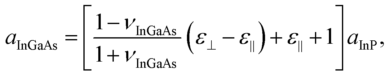 | (1) |
 | ||
| Fig. 1 (a) Schematic layer structure of the as-grown the extended In0.83Ga0.17As photodetector structure, (b) 45 × 45 μm2 AFM image for 750 nm-thick n+-InAs0.63P0.37 topmost buffer, (c) the corresponding height profiles, and (d) asymmetric reciprocal space map of InP (115) reflection. The vertical dashed line and the tilted solid line indicate coherent growth to the InP substrate and full relaxation, respectively. | ||
Fig. 2a shows the schematic of a dielectric multilayered LVOF based on an F–P resonator with distributed Bragg reflectors (DBRs). The LVOF consists of Si and SiO2 dielectric film stacks with refractive indices nSi = 3.523 and nSiO2 = 1.455, respectively. The two DBRs based on Si/SiO2 pairs were considered quarter-wave stacks with a high refractive index contrast of Δn = 2.068. The reflectivity at normal incidence of the Si/SiO2 DBR is given by the following relation:18
 | (2) |
 | (3) |
 , where φ1 and φ2 denote the phase shifts related to the reflection off the top and bottom DBRs, respectively, and λ is the incident wavelength. In Fig. 2b, eight sharp F–P resonance peaks associated with the fundamental resonant mode (m = 1) appear in the spectral range of 1.7–2.4 μm. Undesired higher-order F–P harmonics are present in the transmission spectra ranging from 1.0 to 1.4 μm. A Si/SiO2 blocking filter with an optical density of three was designed to suppress unwanted harmonics. The LVOF shows the fundamental resonance peaks with high transmission greater than 95% and full-width-at-half maximum (FWHM) less than 84 nm in the spectral range of 1.6–2.6 μm when assembled with the designed blocking filter (Fig. 2c).
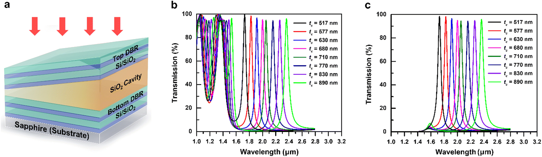 | ||
| Fig. 2 (a) Schematic structure of the Fabry–Perot type linear variable optical filter and simulated transmission spectra for different SiO2 cavity thicknesses ranging from 517 to 890 nm (b) without and (c) with the Si/SiO2 blocking filter. | ||
A vertically tapered optical filter is typically fabricated using a chemical–thermal photoresist reflow process.21 A specially patterned photoresist on a dielectric cavity layer was placed in a sealed chamber saturated with solvent vapor, followed by heat treatment at temperatures higher than the glass transition temperature to reshape the resist owing to the surface tension of the melted resist. However, this reflow process suffers from the difficulty of precisely controlling the solvent vapor condensation and cross-linking reactions of the resist at elevated temperatures. To avoid the disadvantages of the chemical–thermal reflow process, we devised and used an electron beam evaporator with a specially designed linear motion shutter located 8 cm underneath the substrate holder for the fabrication of a Si/SiO2 F–P LVOF (Fig. 3a). A bottom DBR consisting of two pairs of Si (145 nm)/SiO2 (380 nm) layers was deposited on a sapphire substrate. Fig. 3b shows a contour plot of the measured SiO2 cavity thickness as a function of the shutter speed and the horizontal position of the cavity. A shutter speed of 0.33 mms−1 and SiO2 deposition rate of 1.5 Å s−1 were used to obtain a cavity thickness profile linearly increasing from 517 to 890 nm along the horizontal axis of the cavity. After cavity deposition, the linear motion shutter was returned to the initial position, and a Si/SiO2 top DBR was deposited on the tilted SiO2 cavity.
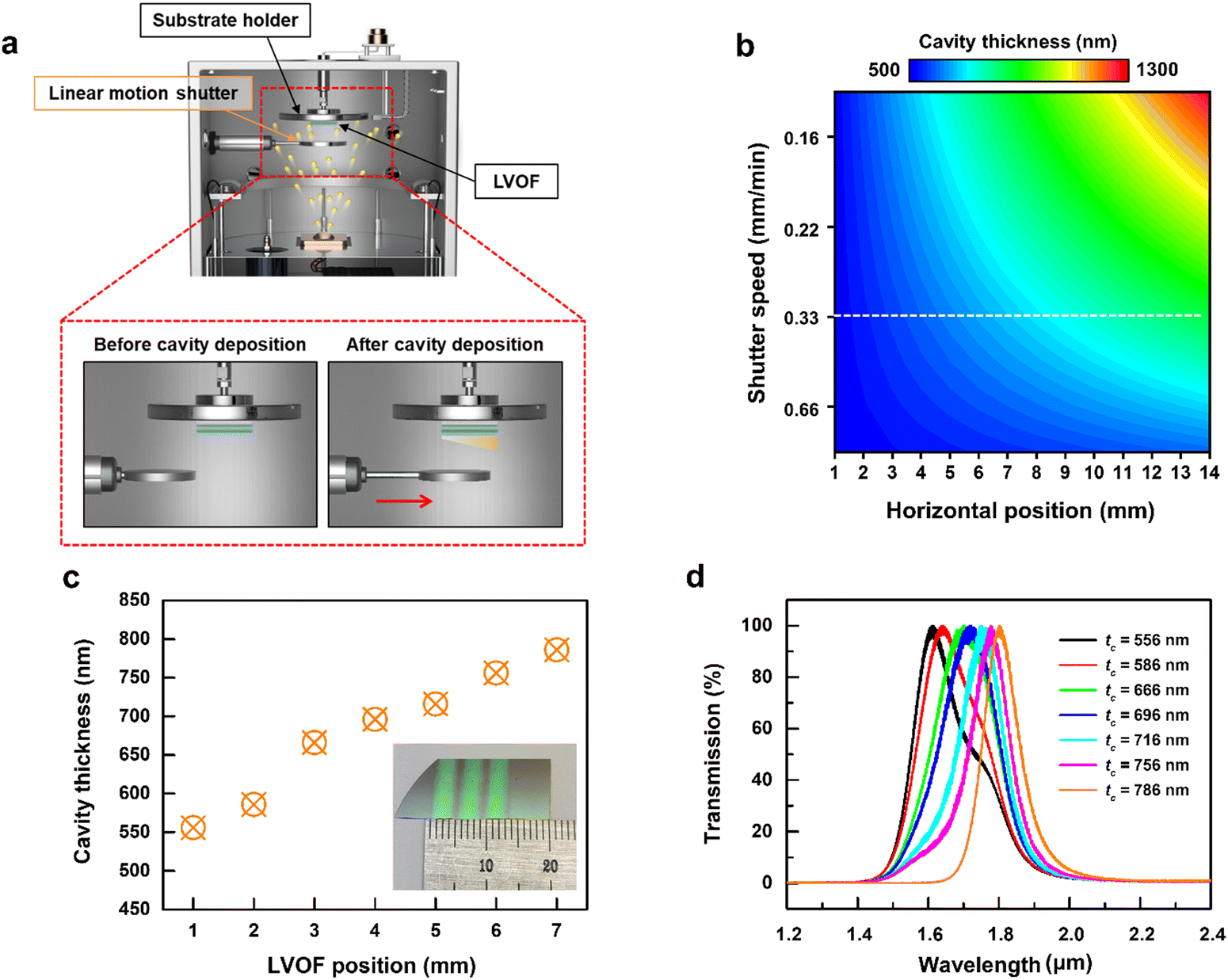 | ||
| Fig. 3 (a) Schematic representation of electron beam evaporation of a tapered SiO2 cavity by using a specially designed linear motion shutter, (b) measured contour plot of the cavity thickness against shutter speed and horizontal position of the cavity, (c) fabricated Si/SiO2 F-P LVOF with a tapered thickness profile, and (d) measured transmission spectra of the fabricated LVOF with varying SiO2 cavity thickness. | ||
Fig. 3c shows the measured SiO2 cavity thickness of an LVOF fabricated on a sapphire substrate according to the position on the LVOF. The transmission spectra of the LVOF were measured with a narrow entrance slit of 50 μm width located between the LVOF and the IR source beam of the Fourier-transform infrared (FT-IR) spectrometer. As seen in Fig. 3d, the peak wavelength of the LVOF increases with increasing cavity thickness due to the fundamental F–P resonance mode. The FWHM of the transmission spectra was measured to be between 120 and 210 nm, which is at least 1.8 times broader than that expected from the simulation shown in Fig. 2c. The divergence angle at the entrance slit was linearly proportional to the incident wavelength (λ). Additionally, the beam diameter after passing through the slit increased because the Rayleigh range decreased with an increase in the incident wavelength.22 In the case of λ = 1.9 μm and the axial distance of 5 mm between the entrance slit and the LVOF, the beam diameter after passing through the slit is estimated to be approximately 250 μm. Such a beam divergence effect causes FWHM broadening of the transmission spectra as a result of the superposition of neighboring F–P transmission modes.
The fabrication of a single-chip SWIR microspectrometer began with the monolithic deposition of vertically tapered layers of Si/SiO2 F–P LVOF on an epitaxial wafer of the extended InGaAs photodetectors, as shown in Fig. 4a. A 6 μm-thick AZ10XT photoresist layer was spun and patterned to prepare an array of 256 × 1 LVOF pixels on the p+-InGaAs top contact layer using conventional photolithography. An LVOF pixel pitch of 50 μm and pixel area of 36 × 470 μm2 were defined by ICP-RIE etching of the LVOF layers under a gas mixture of Ar/SF6 = 50/100 sccm. An array of 256 × 1 extended InGaAs photodetector pixels with a pitch of 50 μm and area of 40 × 500 μm2 was thereafter fabricated underneath the LVOF array using photoresist patterning and ICP-RIE etching with BCl3 gas of 60 sccm (Fig. 4b). The sidewall surface damage caused by the dry etch was removed using a gentle wet etch in a H3PO4![[thin space (1/6-em)]](https://www.rsc.org/images/entities/char_2009.gif) :H2O2:H2O (1:2:20) solution, followed by plasma-enhanced chemical vapor deposition of 200 nm-thick SiO2 as a surface passivation layer (Fig. 4c). The SiO2 opening area was thereafter etched using ICP-RIE with a gas mixture of Ar/CF4 = 30/90 sccm to expose the top and bottom contact layers. The contact metals Pd (6 nm)/Ti (30 nm)/Cr (50 nm)/Au (300 nm) and Pd (25 nm)/Ge (30 nm)/Au (300 nm) were deposited on the top and bottom contact layers by electron beam evaporation, respectively (Fig. 4d). The gaps between the LVOF-integrated detector pixels in the array were filled with a 400 nm-thick Au layer to prevent optical crosstalk between adjacent pixels (Fig. 4e). The top contact metal pads were connected to a silicon readout integrated circuit by Au wiring for the accumulation of photocurrent from each detector pixel and the generation of output signals for the readout (Fig. 4f).
:H2O2:H2O (1:2:20) solution, followed by plasma-enhanced chemical vapor deposition of 200 nm-thick SiO2 as a surface passivation layer (Fig. 4c). The SiO2 opening area was thereafter etched using ICP-RIE with a gas mixture of Ar/CF4 = 30/90 sccm to expose the top and bottom contact layers. The contact metals Pd (6 nm)/Ti (30 nm)/Cr (50 nm)/Au (300 nm) and Pd (25 nm)/Ge (30 nm)/Au (300 nm) were deposited on the top and bottom contact layers by electron beam evaporation, respectively (Fig. 4d). The gaps between the LVOF-integrated detector pixels in the array were filled with a 400 nm-thick Au layer to prevent optical crosstalk between adjacent pixels (Fig. 4e). The top contact metal pads were connected to a silicon readout integrated circuit by Au wiring for the accumulation of photocurrent from each detector pixel and the generation of output signals for the readout (Fig. 4f).
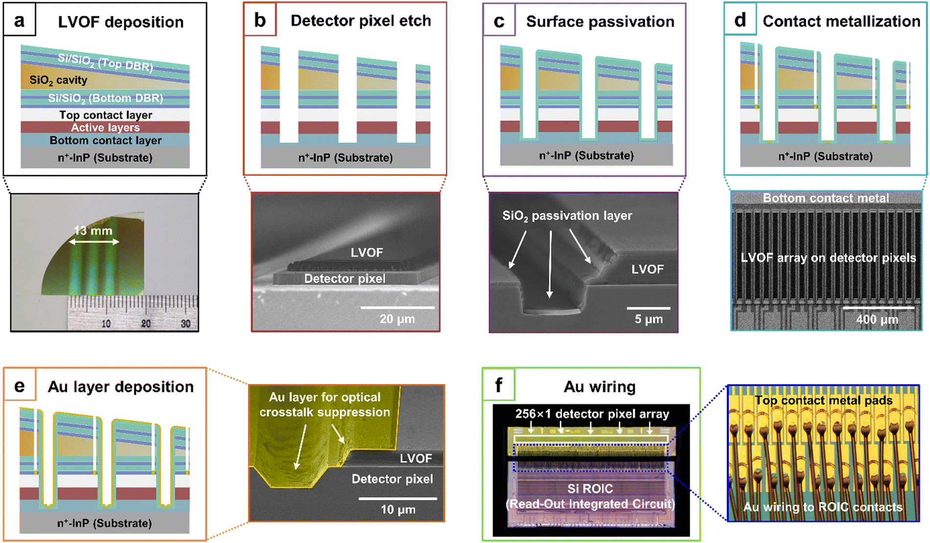 | ||
| Fig. 4 Fabrication flow of a single-chip SWIR microspectrometer. Digital image of (a) a tapered Si/SiO2 F-P LVOF deposited on an extended InGaAs photodetector wafer and scanning electron microscopy (SEM) images of (b) detector pixels integrated with LVOF after ICP-RIE etching, (c) sidewalls of the etched detector pixels surface passivated with 200 nm-thick SiO2, (d) individual top contact pads and a common bottom contact pad of the detector pixels and (e) deposited Au layer for the suppression of light spreading across the inter-pixel gaps, and digital image of (f) 256 × 1 extended InGaAs detector pixel array interconnected to a silicon readout integrated circuit by Au wiring. | ||
Fig. 5a shows the spectral response of an extended SWIR InGaAs reference photodetector without Si/SiO2 F–P LVOF measured at a voltage bias of Vb = 0 V and 300 K. The reference detector had a response peak at ∼2.3 μm with a 90% cutoff wavelength of 2.6 μm. Representative spectral responses of the 256 × 1 extended InGaAs detector pixel array integrated with the LVOF (single-chip SWIR microspectrometer) are measured at Vb = 0 V and 300 K, as shown in Fig. 5b. It is evident that the single-chip SWIR microspectrometer with the Au layer deposited on the inter-pixel gaps has a higher spectral response intensity at the transmission peak wavelength of the LVOF with a SiO2 cavity thickness of 870 nm than that without it. The LVOF transmission, which is equivalent to a wedge etalon, is obtained as follows:23
 | (4) |
 , where x denotes the lateral distance between the LVOF pixel and the wedge apex and α is the wedge angle of ∼2.4°. As shown in Fig. 4e, the top surface of the LVOF was partially covered by the Au layer, with a total coverage of ∼42%. Accordingly, the amount of incident radiation falling on the LVOF diminishes, leading to a lower reflective cavity surface. The reduced reflectivity of the cavity surface directly translates into increased transmission intensity because the fraction of the total intensity lost through the multiple-beam interference by beam walk-off becomes smaller. The beam walk-off is lower owing to the reduction in multiple reflections between the unparallel DBRs of the LVOF.24 Consequently, the peak intensity of the spectral response for the LVOF was higher when the Au layer of the single-chip SWIR microspectrometer was introduced. Fig. 5c shows the measured spectral responses of the single-chip SWIR microspectrometer with the Au layer under zero bias at 300 K. Clearly, the peak wavelength of the spectral response passing through the LVOF increased linearly from 1.665 to 2.065 μm with increasing SiO2 cavity thickness from tc = 602 to 997 nm. As shown in Fig. 2, the linear increase in the peak wavelength with cavity thickness is explained by the peak wavelength dependence on the optical thickness of the cavity (λp ∝ nSiO2tc).
 | ||
| Fig. 5 Measured spectral responses under zero bias at 300 K of (a) an SWIR InGaAs photodetector without Si/SiO2 F-P LVOF, (b) single-chip SWIR microspectrometer without and with the Au layer deposited on the inter-pixel gaps, and (c) single-chip SWIR microspectrometer with the Au layer with increasing SiO2 cavity thickness from top to bottom. | ||
Fig. 6a shows the measured dark current density–voltage (Jd − V) characteristics of the single-chip SWIR microspectrometer in the temperature range of 77–300 K. The Jd − V characteristics are strongly temperature-dependent and represent an exponential increase in the current density with the reverse voltage bias. In Fig. 6b, an Arrhenius plot of the dark current density versus the inverse temperature at Vb = −20 mV provides a route to determine the dominant dark current mechanism. The thermal activation energy (Ea) for the dark current density was extracted from the slope of the Arrhenius plot using the relation Jd(T) = A*T2e−Ea/kBT, where A* denotes the Richardson constant, T is the temperature, and kB is the Boltzmann constant.25 The activation energy was determined to be Ea = 0.214 eV in the temperature range of 180 K < T < 300 K. This value is close to half of the bandgap energy (0.47 eV) of the n-In0.83Ga0.17As absorber, indicating that the reverse dark current is dominated by the generation–recombination (G–R) current mechanism. The Shockley–Read–Hall (SRH) G–R current can be attributed to deep-level traps induced by misfit dislocations at the InGaAs/InAsP heterointerface.26 Such crystalline defects decrease the minority carrier lifetime in the depletion region, which is inversely proportional to the G–R current.27 The band structure at the heterojunction interface was calculated at T = 300 K and Vb = −20 mV using a self-consistent one-dimensional Schrödinger–Poisson solver, as shown in the inset of Fig. 6b.28 The potential energy barriers for electrons and holes were estimated to be ΔEc = 155 meV and ΔEv = 240 meV, respectively. The high-energy barriers effectively suppress the diffusion current over a relatively high-temperature range. In Fig. 6c, the peak responsivity (R) and noise voltage of the single-chip SWIR microspectrometer are plotted as a function of the voltage bias to evaluate the specific detectivity at 300 K. The peak responsivity was derived from the measured rms photocurrent divided by the integral of the product of the spectral photon given wavelength range.29 The responsivity increased exponentially with increasing reverse bias and reached a saturation level at R ≈ 2 AW−1 because of the saturated drift velocity of the photogenerated carriers in a high electric field. Fig. 6d shows the specific detectivity (D*) as a function of the voltage bias at 300 K. D* is determined by the relation  , where R denotes the responsivity, Ad is the active area of the detector pixel, Δf is the bandwidth, and in is the noise current given by dividing the noise voltage by the dynamic resistance of the pixel.30 The highest detectivity of D* = 6.3 × 108 cm Hz1/2 W−1 is achieved at zero bias, with a corresponding responsivity of R = 0.34 A W−1, as shown in Fig. 6d. This detectivity value is relatively lower than the measured detectivity of D* = 5.2 × 109 cm Hz1/2 W−1 for the detector pixel without the LVOF owing to the absorption in the LVOF. In addition, the detectivity decreases with increasing voltage bias because of the highly increased noise voltage induced by the increase in the dark current.
 | ||
| Fig. 6 (a) Dark current density versus voltage curves of the single-chip SWIR microspectrometer measured at 77–300 K, (b) Arrhenius plot for the current density under a voltage bias of −20 mV. The dotted line through the data points is a linear fit to the Arrhenius' equation using a least-squares fitting method. The inset shows the calculated band structure of the InGaAs/InAsP interface at 300 K and −20 mV. (c) responsivity and noise voltage, and (d) specific detectivity measured as a function of voltage bias at 300 K. | ||
3. Conclusion
In conclusion, we have demonstrated an extended SWIR microspectrometer by monolithic integration of a 256 × 1 InGaAs linear array detector with a wedge-shaped Si/SiO2 F–P LVOF. The step-graded metamorphic layers of InAsyP1−y enabled the growth of the p+-InAs0.63P0.37/n-In0.83Ga0.17As heterostructure with a 90% cutoff wavelength of 2.6 μm through a high degree of strain relaxation of ∼96%. The wedge-shaped LVOF fabricated on a sapphire substrate exhibits bandpass filter characteristics, whose transmission peak wavelength increases linearly with the optical thickness of the SiO2 cavity. Similarly, the single-chip microspectrometer consisting of the wedge-shaped LVOF integrated with the 256 × 1 InGaAs detector pixel array yielded a wavelength-tunable bandpass filtering response in the spectral range of 1.6–2.6 μm. The temperature-dependent dark current characteristics of the microspectrometer indicate that at temperatures of 180–300 K, the dominant dark current mechanism is the G–R dark current via SRH recombination in the depletion region, whereas the diffusion dark current is suppressed by the high potential barriers at the p+-InAsP/n-InGaAs heterointerface. The measured responsivity and noise voltage of the microspectrometer are 0.34 AW−1 and 76 nV Hz−1/2 at 300 K under zero bias, respectively, corresponding to a specific detectivity of 6.3 × 108 cm Hz1/2W−1. This novel microspectrometer-on-chip for the extended SWIR region opens interesting possibilities for in-line and real-time monitoring applications.4. Experimental section
Growth of extended InGaAs photodetectors
An extended SWIR InGaAs photodetector structure was grown on a 2-inch (001) n+-InP substrate using a metal–organic chemical vapor deposition system (Veeco D180). For the group-III precursors, trimethylindium (TMIn) and trimethylgallium (TMGa) were used with a H2 carrier gas, whereas arsine (AsH3) and phosphine (PH3) gases were employed as group-V precursors. The dopant precursors for p- and n-type doping were diethylzinc (DEZn) and disilane (Si2H6), respectively. As shown in Fig. 1a, compositionally step-graded n+-InAsyP1−y metamorphic buffer structures were designed and grown to gradually increase the lattice constant from n+-InP to n+-InAs0.63P0.37, serving as a virtual substrate with the desired lattice constant and a bottom contact layer. A 3 μm-thick n-In0.83Ga0.17As absorber with bandgap energy of 0.47 eV was lattice-matched grown on the n+-InAs0.63P0.37 layer, followed by a growth of a 200 nm-thick p+-InAs0.63P0.37 layer. The p+-n heterostructure was capped with a 50 nm-thick p+-In0.83Ga0.17As top contact layer.Transmission simulation
Essential Macleod software was used to design the F–P type LVOF operating in the SWIR region of 1.6–2.6 μm. The optical transmission characteristics of Si/SiO2 LVOF with various SiO2 cavity thicknesses were simulated and analyzed.Fabrication of extended InGaAs linear array detector integrated with LVOF
A wedge-shaped LVOF consisting of a SiO2 resonant cavity with linearly varying thickness sandwiched between two Si/SiO2 reflectors was fabricated on a sapphire substrate using a modified electron beam evaporator. In addition, for the fabrication of an LVOF-integrated 256 × 1 InGaAs linear array detector, wedge-shaped Si/SiO2 multilayers were first deposited on top of an epitaxial wafer of the extended InGaAs detectors and processed into a linear array of 256 detector pixels with a 50 μm pixel pitch and 36 × 470 μm2 pixel area using conventional photolithography and lift-off techniques.Characterization
AFM was used to characterize the surface morphology and roughness of the InAsP metamorphic buffers using non-contact mode AFM (XE-150, Park Systems). High-resolution XRD measurements were performed on the as-grown structure using a Philips X’Pert diffractometer equipped with a CuKα1 X-ray source (λCuKα1 = 1.5406 Å) and a four-bounce (220) Ge monochromator. The thickness profiles of the LVOF were measured using a Veeco Dektak 150 surface profiler. Field-emission SEM (FEI Quanta 650) was used to image the fabricated InGaAs photodetector array integrated with the LVOF. The dark current density–voltage characteristics of the photodetector array were measured at temperatures from 77 to 300 K using a Keithley 236 source measure unit. The spectral responses of the photodetector array were measured at 300 K using the FT-IR spectrometer (Nicolet 5700). The responsivity and detectivity of the detector were measured at 300 K by illuminating the detector with infrared light from a 900 K blackbody source chopped at 400 Hz. The photocurrent and signal noise were measured using a Keithley 428 current amplifier and an SR770 fast Fourier transform network analyzer, respectively.Conflicts of interest
There are no conflicts to declare.Acknowledgements
This research was supported by Nano·Material Technology Development Program through the National Research Foundation of Korea (NRF) funded by Ministry of Science and ICT (NRF-2018M3A7B4069994). This research was supported by National R&D Program through the National Research Foundation of Korea (NRF) funded by Ministry of Science and ICT (2022M3I8A2079227 and NRF-2022M3H4A1A02076394).References
- F. Goetz, G. Vane, J. E. Solomon and B. N. Rock, Science, 1985, 228, 1147 CrossRef PubMed.
- S. K. von Bueren, A. Burkart, A. Hueni, U. Rascher, M. P. Tuohy and I. J. Yule, Biogeosciences, 2015, 12, 163 CrossRef.
- H. S. Choi and H. K. Kim, Nat. Biomed. Eng., 2020, 4, 245 CrossRef PubMed.
- D. Krupnik and S. Khan, Earth-Sci. Rev., 2019, 198, 102952 CrossRef CAS.
- H. L. Shen, Z. H. Zheng, W. Wang, X. Du, S. J. Shao and J. H. Xin, Appl. Opt., 2012, 51, 2616 CrossRef PubMed.
- Q. Li, X. He, Y. Wang, H. Liu, D. Xu and F. Guo, J. Biomed. Opt., 2013, 18, 100901 CrossRef PubMed.
- J. F. Cheng, X. Li, X. M. Shao, T. Li, Y. J. Ma, Y. Gu, S. Y. Deng, Y. G. Zhang and H. M. Gong, IEEE Photonics Technol. Lett., 2022, 34, 231 CAS.
- M. M. P. Arnob, H. Nguyen, Z. Han and W. C. Shih, Appl. Opt., 2018, 18, 5019 CrossRef PubMed.
- H. Cong, C. Xue, J. Zheng, F. Yang, K. Yu, Z. Liu, X. Zhang, B. Cheng and Q. Wang, IEEE Photonics J., 2016, 8, 1 Search PubMed.
- C. Williams, G. S. Gordon, T. D. Wilkinson and S. E. Bohndiek, ACS Photonics, 2019, 6, 3132 CrossRef CAS PubMed.
- A. Emadi, H. Wu, S. Grabarnik, G. De Graaf, K. Hedsten, P. Enoksson, J. H. Correia and R. F. Wolffenbuttel, Sens. Actuators, A, 2010, 162, 400 CrossRef CAS.
- V. E. Brando and A. G. Dekker, IEEE Trans. Geosci. Remote Sens., 2003, 41, 1378 CrossRef.
- Z. Xuan, Q. Liu, Z. Cui, S. Huang, B. Yang, C. Li, S. Wang and W. Lu, Chin. Opt. Lett., 2022, 20, 061302 CrossRef.
- Z. Xuan, Z. Wang, Q. Liu, S. Huang, B. Yang, L. Yang, Z. Yin, M. Xie, C. Li, J. Yu, S. Wang and W. Lu, Opt. Mater., 2022, 10, 2200284 CrossRef CAS.
- V. Holý, J. H. Li, G. Bauer, F. Schäffler and H. J. Herzog, J. Appl. Phys., 1995, 78, 5013 CrossRef.
- V. Swaminathan and A. T. Macrander, Materials aspects of GaAs and InP based structures, Prentice Hall, Inc., 1991 Search PubMed.
- M. K. Hudait, Y. Lin and S. A. Ringel, J. Appl. Phys., 2009, 105, 061643 CrossRef.
- E. F. Schubert, J. K. Kim and J. Q. Xi, Phys. Status Solidi B, 2007, 244, 3002 CrossRef CAS.
- H. Zhu, J. J. He, L. Shao and M. Li, Sens. Actuators, B, 2018, 277, 152 CrossRef CAS.
- S. Zhang, W. Bin, B. Xu, X. Zheng, B. Chen, X. Lv and W. Hofmann, Nanoscale Res. Lett., 2019, 14, 1 CrossRef PubMed.
- A. Emadi, H. Wu, S. Grabarnik, G. De Graaf and R. F. Wolffenbuttel, J. Micromech. Microeng., 2009, 19, 074014 CrossRef.
- D. Meschede, Optics, light and lasers: the practical approach to modern aspects of photonics and laser physics, Wiley-VCH, 2007 Search PubMed.
- M. A. Rob, Opt. Lett., 1990, 15, 604 CrossRef CAS PubMed.
- N. P. Ayerden, G. de Graaf and R. F. Wolffenbuttel, Opt. Express, 2016, 24, 2981 CrossRef CAS PubMed.
- J. H. Lee, Z. M. Wu, Y. M. Liao, Y. R. Wu, S. Y. Lin and S. C. Lee, J. Appl. Phys., 2013, 114, 244504 CrossRef.
- X. Ji, B. Liu, Y. Xu, H. Tang, X. Li, H. Gong, B. Shen, X. Yang, P. Han and F. Yan, J. Appl. Phys., 2013, 114, 224502 CrossRef.
- L. Zimmermann, J. John, S. Degroote, G. Borghs, C. Van Hoof and S. Nemeth, Appl. Phys. Lett., 2003, 82, 2838 CrossRef CAS.
- Nextnano3 software v.4.2.7.9, accessed: April, 2020, https://www.nextnano.de/nextnano3 Search PubMed.
- T. Le, C. P. Morath, H. E. Norton, D. A. Cardimona, S. Raghavan, P. Rotella, S. A. Stintz, B. Fuchs and S. Krishna, Infrared Phys. Technol., 2003, 44, 517 CrossRef.
- T. Li, D. J. H. Lambert, M. M. Wong, C. J. Collins, B. Yang, A. L. Beck, U. Chowdhury, R. D. Durpuis and A. J. Campbell, IEEE J. Quantum Electron., 2001, 37, 538 CrossRef CAS.
Footnote |
| † These authors contributed equally to this work. |
| This journal is © The Royal Society of Chemistry 2023 |