
Superior high temperature performance of 8 kV NiO/Ga2O3 vertical heterojunction rectifiers
Jian-Sian
Li
a,
Chao-Ching
Chiang
a,
Xinyi
Xia
a,
Hsiao-Hsuan
Wan
a,
Fan
Ren
a and
S. J.
Pearton
 *ab
*ab
aDepartment of Chemical Engineering, University of Florida, Gainesville, FL 32606, USA
bDepartment of Materials Science and Engineering, University of Florida, Gainesville, FL 32606, USA. E-mail: spear@mse.ufl.edu
First published on 15th May 2023
Abstract
NiO/β-Ga2O3 vertical rectifiers exhibit near-temperature-independent breakdown voltages (VB) of >8 kV to 600 K. For 100 μm diameter devices, the power figure of merit (VB)2/RON, where RON is the on-state resistance, was 9.1 GW cm−2 at 300 K and 3.9 GW cm−2 at 600 K. By sharp contrast, Schottky rectifiers fabricated on the same wafers show VB of ∼1100 V at 300 K, with a negative temperature coefficient of breakdown of 2 V K−1. The corresponding figures of merit for Schottky rectifiers were 0.22 GW cm−2 at 300 K and 0.59 MW cm−2 at 600 K. The on–off ratio remained >1010 up to 600 K for heterojunction rectifiers but was 3 orders of magnitude lower over the entire temperature range for Schottky rectifiers. The power figure of merit is higher by a factor of approximately 6 than the 1-D unipolar limit of SiC. The reverse recovery times were ∼26 ± 2 ns for both types of devices and were independent of temperature. We also fabricated large area, 1 mm2 rectifiers. These exhibited VB of 4 kV at 300 K and 3.6 kV at 600 K. The results show the promise of using this transparent oxide heterojunction for high temperature, high voltage applications.
Introduction
Ultra-wide bandgap semiconductors with bandgaps > 3.4 eV include diamond, AlN and Ga2O3 and have the potential for significantly higher voltage operation with lower switching losses than commercially available SiC and GaN power devices. The various polytypes of Ga2O3 are attracting attention for their potential application in power switching, solar-blind UV detectors and lateral transistors with enhanced two-dimensional electron gas densities.1–8 It is relatively easy to grow bulk crystals of the stable monoclinic β-polymorph from the melt, which enables large-diameter, high-quality substrates for homoepitaxy at potentially low cost.2 This is attractive for lower manufacturing costs since the material comprises a significant component of the cost of manufacture.Ga2O3 has a high critical electric field strength, which allows for higher operating voltages and lower switching losses in power electronics.1–6 Its ultrawide bandgap also makes it promising for high temperatures and radiation environment applications. As a result of these advantages, Ga2O3 is being considered for several power electronics applications, including inverters, motor drives, and power supplies. There is particular interest in kV-class vertical rectifiers for use in electric vehicles and their charging infrastructure, as well as power management systems for improved switching efficiency for next generation power grids and efficiently interfacing renewable energy sources with these grids.1,4,5 One of the goals is to achieve a high breakdown voltage and low on resistance, which is a benefit for rectifiers because of lower switching losses. A figure of merit for power electronic devices is defined as (VB)2/RON, where VB is the reverse breakdown voltage and RON- is the on-state resistance.1,3,4 To achieve a high-power figure of merit, a rectifier must have a low drift layer concentration, with high electron mobility, as well as low RON, and optimized edge termination to prevent current crowding.1,5–21 The breakdown voltage is larger for thicker drift layers, but this degrades the on-resistance. In addition, vertical geometry devices are desirable, because of their higher power conversion efficiency and absolute currents compared to lateral devices.1,3–5 Power rectifiers are also building blocks for many advanced power handling systems.
The lack of a practical p-type doping capability for Ga2O3 has led to integration with p-type oxides to form p-n heterojunctions with the n-type Ga2O3.9–16 The most successful of these has been NiO, generally deposited by sputtering. The forward current transport mechanism in such junctions is typically recombination at low biases and trap-assisted tunneling at higher bias.10,21–26 Promising rectifier performance has been reported with this approach,14–36 including VB of 8.32 kV, with figure of merit 13.2 GW cm−2.15
A less studied aspect has been the elevated temperature performance of such devices.37–42 In this paper we report an investigation of the temperature dependence of the performance of NiO/Ga2O3 and also co-fabricated Au/Ni/Ga2O3 vertical rectifiers on the same wafers. While the breakdown voltage of the latter fall-off quickly with increasing temperature, the heterojunction rectifiers exhibit nearly temperature-independent VB to 600 K. While we focused on small area devices (100μ), we also fabricated a large area device (1 mm2) to examine the scaling properties.
Experimental
We made both vertical geometry Schottky rectifiers and NiO/Ga2O3 rectifiers on the same wafers. The bilayer NiO thickness of 10/10 nm and the length of the NiO extension beyond the top contact (12 μm) to form the field plate-like overhang were held constant.17 The drift region thickness was 10 μm and these layers were grown by halide vapor phase epitaxy (HVPE) on a (001) Sn-doped (1019 cm−3) β-Ga2O3 single crystal substrate. The samples were purchased from Novel Crystal Technology, Japan. A schematic of the two device structures is shown in Fig. 1 (top).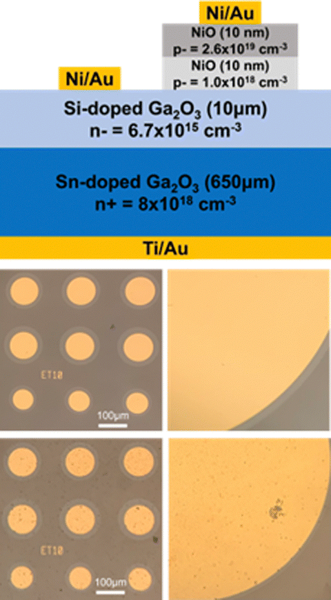 | ||
| Fig. 1 (top) Schematic of the structures and images of devices (center) before and (bottom) after operation at 600 K. | ||
Ohmic contacts were made to the back of the doped substrates using a Ti/Au deposited by e-beam evaporation and annealed at 550 °C for 180 s under N2. The front surface was cleaned by UV/Ozone exposure for 15 mins to remove contamination.17 The 10/10 nm NiO bilayer was deposited after the Ohmic contacts by rf (13.56 MHz) magnetron sputtering at a working pressure of 3 mTorr. The hole concentration in these films was adjusted using the Ar/O2 ratio. The structure was then annealed at 300 °C under O2. Finally, a top contact of 20/80 nm Ni/Au (100 μm or 1 mm diameter) was deposited onto the NiO layer and also formed the Schottky contact on those devices. The NiO was extended 12 μm beyond the contact metal to form a field-plate-like overhang. C−2–V plots for the drift layer doping showed that the carrier concentration was 6.7 × 1015 cm−3. The device design for NiO thickness and extension was guided by TCAD simulations.17
The current density–voltage (J–V) characteristics were measured on Tektronix 370-A and 371-B curve tracers and an Agilent 4156C parameter analyser. For the reverse voltages >2 kV, a Glassman power supply was employed and all the measurements were performed in a Fluorinert atmosphere to avoid breakdown of the air at these high voltages. The reverse breakdown voltage was defined as the bias for a reverse current reaching 0.1 A cm2. The devices did not suffer permanent damage under these conditions, with identical I–V characteristics as before measurement, but increasing the voltage a further 50–200 V led to permanent failure through breakdown at the NiO/Ga2O3 contact periphery. The on-resistance values were calculated assuming that the current spreading length is 10 μm and a 45° spreading angle. We also subtracted the resistance of the cable, probe and chuck, which was around 10 Ohm.
Results and discussion
Fig. 2 shows the forward J–V characteristics and associated on-state resistances from (top) Schottky (SBD) rectifiers and (bottom) heterojunction (HJD) rectifiers of 100 μm diameter as a function of temperature. The on-resistance was obtained from the slope of the forward I–V characteristics. The turn-on voltages decrease with increasing temperature in both types of devices, while RON increases due to the decreased carrier mobility at higher temperatures.4–6 A Richardson plot for the Schottky rectifiers showed a eΦb0 value of 0.6 eV and a Richardson's constant of 40 A cm2 K−1. The barrier height monotonically decreased from 1.02 eV at 300 K to 0.65 eV at 600 K. The RON values are slightly higher for the HJD, as expected.14–17 Both types can conduct >100 A cm−2 at 4 V. Note that the RON in the heterojunction rectifiers does not continue to decrease at forward voltages beyond ∼3 V. It has also been shown that the band alignment remains type II, staggered gap with the magnitude of the conduction and valence band offsets increasing monotonically with annealing temperature.12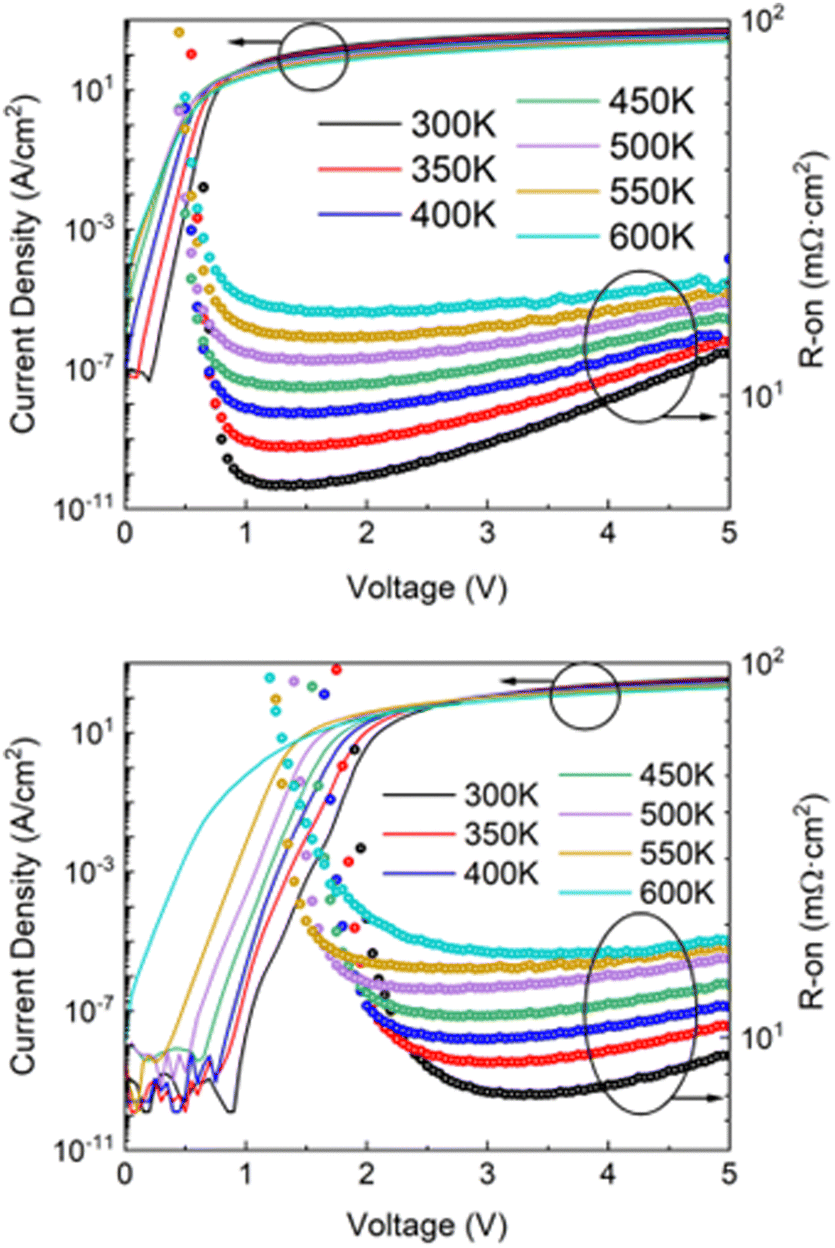 | ||
| Fig. 2 Forward current densities and RON values for (top) Schottky rectifiers or (bottom) NiO/Ga2O3 as a function of temperature. | ||
Fig. 3 shows the reverse J–V characteristics for both types of devices at different temperatures. The Schottky rectifiers show a sharp reduction in the breakdown voltage as temperature increases, as shown in Fig. 3 (top). By sharp contrast, the heterojunction rectifiers show very little change in breakdown voltage, as shown in Fig. 3 (bottom). Note also that the Schottky devices have breakdown voltages of only ∼1100 V at 300 K, whereas the NiO/Ga2O3 devices remain above 8 kV across the temperature range up to 600 K. This is a remarkable demonstration of the utility of NiO in forming a robust p–n junction with Ga2O3 and also in providing effective edge termination to mitigate breakdown at the contact periphery. The devices did not show any visible damage after measurement at 600 K, as shown in the center and bottom of Fig. 1 for the Schottky and heterojunction rectifiers, respectively.
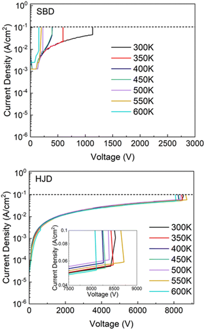 | ||
| Fig. 3 (top) Reverse current characteristics from Schottky rectifiers and (bottom) NiO/Ga2O3 heterojunction rectifiers as a function of temperature. | ||
To give an example of the uniformity of the results, Fig. 4 (top) shows the spread of the reverse current characteristics from eight different NiO/Ga2O3 heterojunction rectifiers at 300 K. This was from 7.9–8.7 kV, measured over an area of approximately 1 cm2. The trends in VB with temperature are shown in Fig. 4 (bottom) for the two device types, with the same number of Schottky diodes measured. While the heterojunction devices show no significant change in VB up to 600 K, the Schottky rectifiers show the commonly reported negative temperature coefficient. The temperature dependence of VB follows an approximate relationship of the form:4,37–42
| VB = VB0[1 + β(T − T0)] |
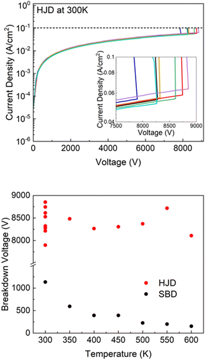 | ||
| Fig. 4 (top) Spread of reverse current characteristics from NiO/Ga2O3 heterojunction rectifiers at 300 K. (bottom) Temperature dependence of breakdown voltage for Schottky barrier diodes and heterojunction diodes. | ||
Fig. 5 shows a compilation of reported maximum operation temperature versus VB for vertical Ga2O3 rectifiers. There is a clear improvement in the present work, which we ascribe to the advances in crystal growth in lowering the drift layer carrier concentration and extended defect density in the starting wafers and also to optimization of the NiO deposition parameters.
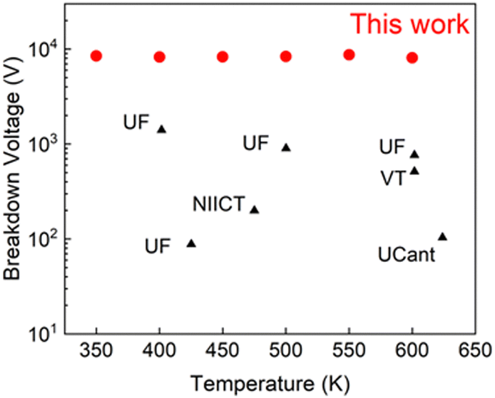 | ||
| Fig. 5 Compilation of maximum operation temperature versus VB for vertical Ga2O3 rectifiers. Previous data comes from Virginia Tech37, University of Canterbury39, University of Florida38 and NIICT40. | ||
The RON and turn-on voltages from the Schottky and heterojunction rectifiers are shown as a function of temperature in Fig. 6. The RON values are higher for the heterojunctions and increase with temperature, which we ascribe mainly to the degradation in carrier mobility through phonon (lattice) scattering since we could fit the RON data to a T3/2 dependence. Additional evidence could come from extracting mobility from the space charge limited current via the Mott–Gurney Law. The turn-on voltage exhibited a weak dependence on temperature and was lower for the Schottky rectifiers, as expected. The power figure of merits for the heterojunctions were 9.1 GW cm−2 at 300 K and 3.9 GW cm−2 at 600 K. Note that the theoretical maximum is around 34 MW cm−2. The corresponding figures of merit for Schottky rectifiers were 0.22 GW cm−2 at 300 K and 0.59 MW cm−2 at 600 K.
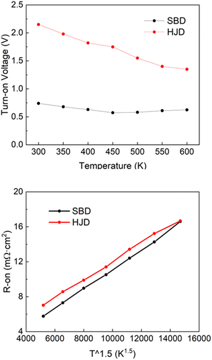 | ||
| Fig. 6 Temperature dependence of on-state resistance and turn-on voltage for Schottky barrier diodes and heterojunction diodes. | ||
The on–off ratios as a function of temperature when switching from 5 V forward bias to the negative voltages shown on the x-axes are shown in Fig. 7 for both types of rectifiers. The values are 1–3 orders of magnitude higher for the heterojunctions due to the lower reverse current at a given bias. Even at 600 K the on–off ratio is ∼109 for the NiO/Ga2O3 rectifiers.
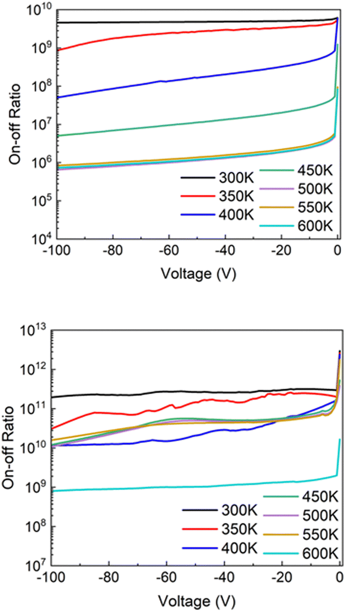 | ||
| Fig. 7 On–off ratio of (top) Schottky rectifiers and (bottom) NiO/Ga2O3 heterojunction rectifiers in which the bias was switched from 5 V forward to the voltage shown on the x-axis. | ||
Fig. 8 shows the temperature dependence of the on/off ratio for (top) Schottky barrier diodes and (bottom) heterojunction diodes for switching from 5 V forward voltage to 0 V. These are essentially the maximum on–off ratios achievable in the devices.
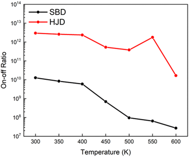 | ||
| Fig. 8 Temperature dependence of the on/off ratio for Schottky barrier diodes and heterojunction diodes when switching from 5 V forward to 0 V. | ||
The switching characteristics of the rectifiers are also of paramount interest, since they need fast recovery times and the ability to switch large currents.45–63Fig. 9 shows the temperature dependence of (top) Schottky rectifiers and (bottom) NiO/Ga2O3 heterojunction rectifiers of reverse recovery characteristics in which the devices were switched from 60 mA forward current to 0 V. The reverse recovery times are ∼ 26 ± 2 ns and are tabulated in Table 1. The relative indifference to device structure and temperature demonstrates that charge storage in the p–n junction is not a significant factor compared to the Schottky device. We have not seen a significant difference in recovery characteristics between small and large devices.
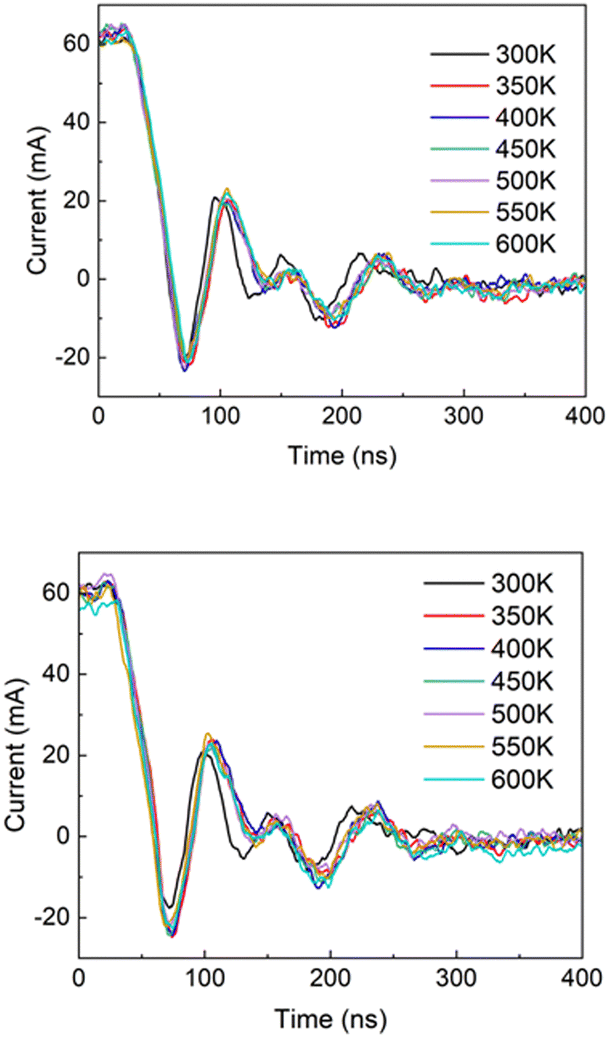 | ||
| Fig. 9 Temperature dependence of switching characteristics of (top) Schottky rectifiers and (bottom) NiO/Ga2O3 heterojunction rectifiers in which the devices were switched from 60 mA forward current to zero. | ||
| Temperature (K) | Trr (ns) | Irr (mA) | dI/dT (A μs−1) | IF (mA) |
|---|---|---|---|---|
| Schottky | ||||
| 300 | 24 | −23 | 2.7 | 60 |
| 350 | 28 | −26 | 2.6 | 60 |
| 400 | 28 | −27 | 2.5 | 60 |
| 450 | 25 | −26 | 2.3 | 60 |
| 500 | 27 | −25 | 2.1 | 60 |
| 550 | 26 | −26 | 2.3 | 60 |
| 600 | 24 | −26 | 2.2 | 60 |
| Heterojunction | ||||
| 300 | 25 | −20 | 2.4 | 60 |
| 350 | 25 | −27 | 2.0 | 60 |
| 400 | 25 | −27 | 2.0 | 60 |
| 450 | 25 | −27 | 1.9 | 60 |
| 500 | 23 | −26 | 1.9 | 60 |
| 550 | 25 | −24 | 1.9 | 60 |
| 600 | 27 | −25 | 1.9 | 60 |
We also examined the temperature dependence of the performance of the large area (1 mm2) heterojunction rectifiers. Fig. 10 (top) shows the forward current characteristics. Note that the absolute forward current is >3 A for all temperatures, with a breakdown voltage of 4 kV at room temperature, as shown in Fig. 10 (bottom). The reason for the lower breakdown is not clear and could be due to a higher probability of having intrinsic defects or an issue with field crowding. The power figure-of-merit is 6.4 GW cm−2 at 300 K and 0.8 MW cm−2 at 600 K. The on–off ratio remained above 108 at 600 K, for switching to −100 V, as shown in Fig. 11.
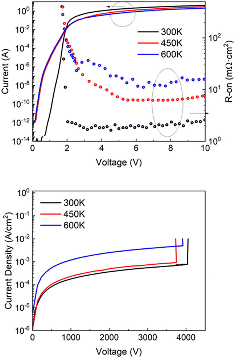 | ||
| Fig. 10 (top) Forward current densities and RON values and (bottom) reverse current characteristics from 1 mm2 NiO/Ga2O3 heterojunction rectifiers as a function of temperature. | ||
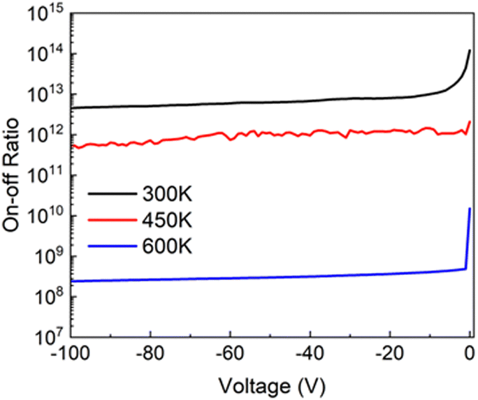 | ||
| Fig. 11 On–off ratio of 1 mm2 NiO/Ga2O3 heterojunction rectifiers in which the bias was switched from 10 V forward to the voltage shown on the x-axis. | ||
Conclusions
Since the breakdown, forward I–V and on resistance did not degrade to much at 300 °C, the concerns of low thermal conductivity of gallium oxide should be of less concern provided the long-term reliability can be established. The power figure of merits reported here are around 26% of the theoretical maximum for Ga2O3.15 It is anticipated that continued reduction in defect density, as well as adding other edge termination technology such as field plates, implanted guard rings, and mesa etching as possible methods to improve field uniformity can enhance future performance closer to this maximum. This is because bulk Ga2O3 crystals are known to have internal planar defects, i.e., plate-like voids and stacking faults, and it is known that higher dislocation densities lead to higher leakage currents in Ga2O3 rectifiers.64–66 This is because the dislocations can act as recombination centers for electrons and holes, leading to an increased probability of carrier recombination and subsequent leakage current and hence lower breakdown voltage.The NiO/Ga2O3 heterojunction rectifier is potentially an ideal structure for high-voltage and high-power applications, where it can offer better efficiency and reduced energy losses compared to traditional semiconductors. The wide bandgap of both NiO (∼3.9 eV) and β-Ga2O3 (4.8 eV) also makes power rectifiers from this heterojunction attractive for high-temperature applications. These properties make Ga2O3 power rectifiers promising for high-power and high-temperature applications such as electric vehicles, power electronics, and aerospace.
Conflicts of interest
There are no conflicts to declare.Acknowledgements
The work at UF was performed as part of the Interaction of Ionizing Radiation with Matter University Research Alliance (IIRM-URA), sponsored by the Department of the Defense, Defense Threat Reduction Agency under award HDTRA1-20-2-0002. The content of the information does not necessarily reflect the position or the policy of the federal government, and no official endorsement should be inferred. The work at UF was also supported by NSF DMR 1856662.References
- M. H. Wong and M. Higashiwaki, IEEE Trans. Electron Devices, 2020, 67, 3925 CAS.
- Z. Galazka, J. Appl. Phys., 2022, 131, 031103 CrossRef CAS.
- X. Lu, Y. X. Deng, Y. L. Pei, Z. M. Chen and G. Wang, J. Semicond., 2023, 44, 061802 Search PubMed.
- A. J. Green, J. Speck, G. Xing, P. Moens, F. Allerstam, K. Gumaelius, T. Neyer, A. Arias-Purdue, V. Mehrotra, A. Kuramata, K. Sasaki, S. Watanabe, K. Koshi, J. Blevins, O. Bierwagen, S. Krishnamoorthy, K. Leedy, A. R. Arehart, A. T. Neal, S. Mou, S. A. Ringel, A. Kumar, A. Sharma, K. Ghosh, U. Singisetti, W. Li, K. Chabak, K. Liddy, A. Islam, S. Rajan, S. Graham, S. Choi, Z. Cheng and M. Higashiwaki, APL Mater., 2022, 10, 029201 CrossRef CAS.
- S. J. Pearton, F. Ren, M. Tadjer and J. Kim, J. Appl. Phys., 2018, 124, 220901 CrossRef.
- C. Wang, J. Zhang, S. Xu, C. Zhang, Q. Feng, Y. Zhang, J. Ning, S. Zhao, H. Zhou and Y. Hao, J. Phys. D: Appl. Phys., 2021, 54, 243001 CrossRef CAS.
- M. Bosi, P. Mazzolini, L. Seravalli and R. Fornari, J. Mater. Chem. C, 2020, 8, 10975 RSC.
- K. Kaneko, K. Uno, R. Jinno and S. Fujit, J. Appl. Phys., 2022, 131, 090902 CrossRef CAS.
- Y. Kokubun, S. Kubo and S. Nakagomi, Appl. Phys. Express, 2016, 9, 091101 CrossRef.
- Y. Deng, Z. Yang, T. Xu, H. Jiang, K. W. Ng, C. Liao, D. Su, Y. Pei, Z. Chen, G. Wang and X. Lu, Appl. Surf. Sci., 2023, 622, 156917 CrossRef CAS.
- M. I. Pintor-Monroy, D. Barrera, B. L. Murillo-Borjas, F. Javier Ochoa-Estrella, J. W. P. Hsu and M. A. Quevedo-Lopez, ACS Appl. Mater. Interfaces, 2018, 10, 38159 CrossRef CAS PubMed.
- X. Xia, J.-S. Li, C.-C. Chiang, T. J. Yoo, F. Ren, H. Kim and S. J. Pearton, J. Phys. D: Appl. Phys., 2022, 55, 385105 CrossRef.
- H. Gong, X. Chen, Y. Xu, Y. Chen, F. Ren, B. Liu, S. Gu, R. Zhang and J. Ye, IEEE Trans. Electron Devices, 2020, 67, 3341 CAS.
- S. Sharma, K. Zeng, S. Saha and U. Singisetti, IEEE Trans. Electron Devices, 2020, 41, 836 CAS.
- J. Zhang, P. Dong, K. Dang, Y. Zhang, Q. Yan, H. Xiang, J. Su, Z. Liu, M. Si, J. Gao, M. Kong, H. Zhou and Y. Hao, Nat. Commun., 2022, 13, 3900 CrossRef CAS PubMed.
- P. Dong, J. Zhang, Q. Yan, Z. Liu, P. Ma, H. Zhou and Y. Hao, IEEE Trans. Electron Devices, 2022, 43, 765 CAS.
- J.-S. Li, C.-C. Chiang, X. Xia, T. Jinsoo Yoo, F. Ren, H. Kim and S. J. Pearton, Appl. Phys. Lett., 2022, 121, 042105 CrossRef CAS.
- Y. Lv, Y. Wang, X. Fu, S. Dun, Z. Sun, H. Liu, X. Zhou, X. Song, K. Dang, S. Liang, J. Zhang, H. Zhou, Z. Feng, S. Cai and Y. Hao, IEEE Trans. Power Electr., 2021, 36, 6179 Search PubMed.
- C. Liao, X. Lu, T. Xu, P. Fang, Y. Deng, H. Luo, Z. Wu, Z. Chen, J. Liang, Y. Pei and G. Wang, IEEE Trans. Electron Devices, 2022, 69, 5722 CAS.
- M. Xiao, B. Wang, J. Liu, R. Zhang, Z. Zhang, C. Ding, S. Lu, K. Sasaki, G.-Q. Lu, C. Buttay and Y. Zhang, IEEE Trans. Power Electr., 2021, 36, 8565 Search PubMed.
- X. Lu, X. Zhou, H. Jiang, K. Wei Ng, Z. Chen, Y. Pei, K. May Lau and G. Wang, IEEE Electron Device Lett., 2020, 41, 449 CAS.
- C. Wang, H. Gong, W. Lei, Y. Cai, Z. Hu, S. Xu, Z. Liu, Q. Feng, H. Zhou, J. Ye, J. Zhang, R. Zhang and Y. Hao, IEEE Electron Device Lett., 2021, 42, 485 CAS.
- Q. Yan, H. Gong, J. Zhang, J. Ye, H. Zhou, Z. Liu, S. Xu, C. Wang, Z. Hu, Q. Feng, J. Ning, C. Zhang, P. Ma, R. Zhang and Y. Hao, Appl. Phys. Lett., 2021, 118, 122102 CrossRef CAS.
- H. H. Gong, X. H. Chen, Y. Xu, F.-F. Ren, S. L. Gu and J. D. Ye, Appl. Phys. Lett., 2020, 117, 022104 CrossRef CAS.
- H. Gong, F. Zhou, W. Xu, X. Yu, Y. Xu, Y. Yang, F.-F. Ren, S. Gu, Y. Zheng, R. Zhang, H. Lu and J. Ye, IEEE Trans. Power Electr., 2021, 36, 12213 Search PubMed.
- H. H. Gong, X. X. Yu, Y. Xu, X. H. Chen, Y. Kuang, Y. J. Lv, Y. Yang, F.-F. Ren, Z. H. Feng, S. L. Gu, Y. D. Zheng, R. Zhang and J. D. Yue, Appl. Phys. Lett., 2021, 118, 202102 CrossRef CAS.
- W. Hao, Q. He, K. Zhou, G. Xu, W. Xiong, X. Zhou, G. Jian, C. Chen, X. Zhao and S. Long, Appl. Phys. Lett., 2021, 118, 043501 CrossRef CAS.
- F. Zhou, H. Gong, W. Xu, X. Yu, Y. Xu, Y. Yang, F.-F. Ren, S. Gu, Y. Zheng, R. Zhang, J. Ye and H. Lu, IEEE Trans. Power Electr., 2022, 37, 1223 Search PubMed.
- Q. Yan, H. Gong, H. Zhou, J. Zhang, J. Ye, Z. Liu, C. Wang, X. Zheng, R. Zhang and Y. Hao, Appl. Phys. Lett., 2022, 120, 092106 CrossRef CAS.
- Y. J. Lv, Y. G. Wang, X. C. Fu, S. B. Dun, Z. F. Sun, H. Y. Liu, X. Y. Zhou, X. B. Song, K. Dang, S. X. Liang, J. C. Zhang, H. Zhou, Z. H. Feng, S. J. Cai and Y. Hao, IEEE Trans. Power Electr., 2021, 36, 6179 Search PubMed.
- J. Zhang, S. Han, M. Cui, X. Xu, W. Li, H. Xu, C. Jin, M. Gu, L. Chen and K. H. L. Zhang, ACS Appl. Electron. Mater., 2020, 2, 456 CrossRef CAS.
- Y. Wang, H. Gong, Y. Lv, X. Fu, S. Dun, T. Han, H. Liu, X. Zhou, S. Liang, J. Ye, R. Zhang, A. Bu, S. Cai and Z. Feng, IEEE Trans. Power Electr., 2022, 37, 3743 Search PubMed.
- J.-S. Li, C.-C. Chiang, X. Xia, H.-H. Wan, F. Ren and S. J. Pearton, J. Vac. Sci. Technol. A, 2023, 41, 030401 CrossRef CAS.
- Z. Wang, H. Gong, S. Member, C. Meng, X. Yu, X. Sun, C. Zhang, X. Ji, F. Ren, S. Gu, Y. Zheng, R. Zhang and J. Ye, IEEE Trans. Electron Devices, 2022, 69, 981 CAS.
- B. Wang, M. Xiao, J. Spencer, Y. Qin, K. Sasaki, M. J. Tadjer and Y. Zhang, IEEE Electron Device Lett., 2023, 44, 221 CAS.
- F. Zhou, H. H. Gong, Z. P. Wang, W. Z. Xu, X. X. Yu, Y. Yang, F.-F. Ren, S. L. Gu, R. Zhang, Y. D. Zheng, H. Lu and J. D. Ye, Appl. Phys. Lett., 2021, 119, 262103 CrossRef CAS.
- B. Wang, M. Xiao, X. Yan, H. Y. Wong, J. Ma, K. Sasaki, H. Wang and Y. Zhang, Appl. Phys. Lett., 2019, 115, 263503 CrossRef.
- X. Xia, M. Xian, P. Carey, C. Fares, F. Ren, M. Tadjer, S. J. Pearton, T. Quang Tu, K. Goto and A. Kuramata, J. Phys. D: Appl. Phys., 2021, 54, 305103 CrossRef CAS.
- C. Hou, K. R. York, R. A. Makin, S. M. Durbin, R. M. Gazoni, R. J. Reeves and M. W. Allen, Appl. Phys. Lett., 2020, 117, 203502 CrossRef CAS.
- S. Ahn, F. Ren, L. Yuan, S. J. Pearton and A. Kuramata, ECS J. Solid State Sci. Technol., 2017, 6, P68 CrossRef CAS.
- M. Higashiwaki, K. Konishi, K. Sasaki, K. Goto, K. Nomura, Q. T. Thieu and R. Togashi, Appl. Phys. Lett., 2016, 108, 133503 CrossRef.
- W. Hao, Q. He, X. Zhou, X. Zhao, G. Xu and S. Long, 2.6 kV NiO/Ga2O3 Heterojunction Diode with Superior High-Temperature Voltage Blocking Capability, 2022 IEEE 34th International Symposium on Power Semiconductor Devices and ICs (ISPSD), Vancouver, BC, Canada, 2022, pp. 105–108.
- L. Cao, Z. Zhu, G. Harden, H. Ye, J. Wang, A. Hoffman and P. Fay, IEEE Trans. Electron Devices, 2021, 68, 1228 CAS.
- E. B. Yakimov, A. Y. Polyakov, I. V. Shchemerov, N. B. Smirnov, A. A. Vasilev, A. I. Kochkova, P. S. Vergeles, E. E. Yakimov, A. V. Chernykh, M. Xian, F. Ren and S. J. Pearton, J. Alloys Compd., 2021, 879, 160394 CrossRef CAS.
- W. Hao, F. Wu, W. Li, G. Xu, X. Xie, K. Zhou, W. Guo, X. Zhou, Q. He, X. Zhao, S. Yang and S. Long, High-Performance Vertical β-Ga2O3 Schottky Barrier Diodes Featuring P-NiO JTE with Adjustable Conductivity, 2022 International Electron Devices Meeting (IEDM), San Francisco, CA, USA, 2022, pp. 9.5.1–9.5.4.
- X. Zhou, Q. Liu, W. Hao, G. Xu and S. Long, Normally-off β-Ga2O3 Power Heterojunction Field-Effect-Transistor Realized by p-NiO and Recessed-Gate, 2022 IEEE 34th International Symposium on Power Semiconductor Devices and ICs (ISPSD), Vancouver, BC, Canada, 2022, pp. 101–104.
- Y. Qin, Z. Wang, K. Sasaki, J. Ye and Y. Zhang, Jpn J. Appl. Phys., 2023, 62, SF0801 CrossRef.
- H. Gong, F. Zhou, W. Xu, X. Yu, Y. Xu, Y. Yang, F. Ren, S. Gu, Y. Zheng and R. Zhang, IEEE Trans. Power Electr., 2021, 36, 12213 Search PubMed.
- J. Yang, C. Fares, R. Elhassani, M. Xian, F. Ren, S. J. Pearton, M. Tadjer and A. Kuramata, ECS J. Solid State Sci. Technol., 2019, 8, Q3159 CrossRef CAS.
- M. Ji, N. R. Taylor, I. Kravchenko, P. Joshi, T. Aytug, L. R. Cao and M. P. Paranthaman, IEEE Trans. Power Electr., 2020, 36, 41 Search PubMed.
- Z. Islam, M. Xian, A. Haque, F. Ren, M. Tadjer and S. J. Pearton, IEEE Trans. Electron Devices, 2020, 67, 3056 CAS.
- R. Sun, A. R. Balog, H. Yang, N. Alem and M. A. Scarpulla, IEEE Electron Device Lett., 2023, 44(5), 725–728 Search PubMed.
- M. Xiao, B. Wang, J. Liu, R. Zhang, R. Zhang, C. Ding, S. Lu, K. Sasaki, G. Q. Lu, C. Buttay and Y. Zhang, IEEE Trans. Power Electr., 2021, 36, 8565 Search PubMed.
- H. Gong, F. Zhou, X. Yu, W. Xu, F. Ren, S. Gu, H. Lu, J. Ye and R. Zhang, IEEE Electron Device Lett., 2022, 43, 773 CAS.
- F. Otsuka, H. Miyamoto, A. Takatsuka, S. Kunori, K. Sasaki and A. Kuramata, Appl. Phys. Express, 2021, 15, 016501 CrossRef.
- W. Hao, F. Wu, W. Li, G. Xu, X. Xie, K. Zhou, W. Guo, X. Zhou, Q. He, X. Zhao and S. Yang, 2022, December. High-Performance Vertical β-Ga2O3 Schottky Barrier Diodes Featuring P-NiO JTE with Adjustable Conductivity. In 2022 International Electron Devices Meeting (IEDM) (pp. 9–5). IEEE.
- Y. Lv, Y. Wang, X. Fu, S. Dun, Z. Sun, H. Liu, X. Zhou, X. Song, K. Dang, S. Liang and J. Zhang, IEEE Trans. Power Electr., 2020, 3, 6179 Search PubMed.
- J. Wei, Y. Wei, J. Lu, X. Peng, Z. Jiang, K. Yang and X. Luo, 2022, May. Experimental Study on Electrical Characteristics of Large-Size Vertical β-Ga2O3 Junction Barrier Schottky Diodes. In 2022 IEEE 34th International Symposium on Power Semiconductor Devices and ICs (ISPSD) (pp. 97–100). IEEE.
- J. Yang, F. Ren, Y.-T. Chen, Y.-T. Liao, C.-W. Chang, J. Lin, M. J. Tadjer, S. J. Pearton and A. Kuramata, IEEE J. Electron Devices Soc., 2019, 7, 57 CAS.
- J.-S. Li, C.-C. Chiang, X. Xia, F. Ren and S. J. Pearton, J. Vac. Sci. Technol., A, 2022, 40, 063407 CrossRef CAS.
- F. Zhou, H. H. Gong, Z. P. Wang, W. Z. Xu, X. X. Yu, Y. Yang, F. F. Ren, S. L. Gu, R. Zhang, Y. D. Zheng and H. Lu, Appl. Phys. Lett., 2021, 119, 262103 CrossRef CAS.
- F. Zhou, H. Gong, W. Xu, X. Yu, Y. Xu, Y. Yang, F. F. Ren, S. Gu, Y. Zheng, R. Zhang and J. Ye, IEEE Trans. Power Electr., 2021, 37, 1223 Search PubMed.
- J. S. Li, C. C. Chiang, X. Xia, C. T. Tsai, F. Ren, Y. T. Liao and S. J. Pearton, ECS J. Solid State Sci. Technol., 2022, 11, 105003 CrossRef.
- S. Sdoeung, K. Sasaki, K. Kawasaki, J. Hirabayashi, A. Kuramata and M. Kasu, Jpn. J. Appl. Phys., 2023, 62, SF1001 CrossRef.
- B. Wang, M. Xiao, J. Knoll, C. Buttay, K. Sasaki, C. Dimarino and Y. Zhang, IEEE Electron Device Lett., 2021, 42, 1132 Search PubMed.
- K. Ogawa, N. Ogawa, R. Kosaka, T. Isshiki, Y. Yao and Y. Ishikawa, J. Electron. Mater., 2020, 49, 5190 CrossRef CAS.
| This journal is © The Royal Society of Chemistry 2023 |