
 Open Access Article
 This Open Access Article is licensed under a
 Creative Commons Attribution 3.0 Unported Licence
Stress induced effects on piezoelectric polycrystalline potassium sodium niobate thin films
Rui
Pinho
a,
Rui
Vilarinho
b,
J. Agostinho
Moreira
 b,
Fátima
Zorro
cd,
Paulo
Ferreira
cde,
Maxim
Ivanov
a,
Alexander
Tkach
a,
M. Elisabete
Costa
a and
Paula M.
Vilarinho
*a
b,
Fátima
Zorro
cd,
Paulo
Ferreira
cde,
Maxim
Ivanov
a,
Alexander
Tkach
a,
M. Elisabete
Costa
a and
Paula M.
Vilarinho
*a
aCICECO – Aveiro Institute of Materials, Department of Materials and Ceramic Engineering, University of Aveiro, Aveiro, 3810-193, Portugal. E-mail: paula.vilarinho@ua.pt
bIFIMUP, Institute of Physics for Advanced Materials, Nanotechnology and Photonics, Department of Physics and Astronomy of Faculty of Sciences, University of Porto, Portugal
cINL – International Iberian Nanotechnology Laboratory, Av. Mestre José Veiga s/n, 4715-330 Braga, Portugal
dMechanical Engineering Department and IDMEC, Instituto Superior Técnico, University of Lisbon, Av. Rovisco Pais, 1049-001 Lisboa, Portugal
eMaterials Science and Engineering Program, The University of Texas at Austin, Tx 78712, USA
First published on 31st May 2023
Abstract
The piezoelectric market is ruled by lead-based compounds that should be substituted by environmentally friendly materials. Despite the substantial literature on lead-free candidates available, stress effects on the dielectric, piezoelectric and ferroelectric performance of thin films from the nano- to macroscale have been barely addressed until now. In this work, a combination of multiscale characterization techniques is used to disclose the induced mechanical deformation impact on the dielectric, polar and structural properties of polycrystalline lead-free potassium sodium niobate (KNN) thin films fabricated on platinized silicon (Pt/Si(100)), strontium titanate (Pt/STO(100)) and magnesium oxide (Pt/MgO(100)) substrates. A tensile residual stress state characterizes KNN films on Pt/Si (+210 ± 28 MPa), while KNN films on Pt/STO and Pt/MgO (−411 ± 18 MPa and −494 ± 26 MPa, respectively) evidence a compressive residual stress condition. Films with the highest compressive state (on Pt/MgO) exhibit the lowest dielectric losses with the highest electric permittivity and the maximum electric polarization; concomitantly they present the most dense and homogeneous microstructure, with small grains and a narrow grain size distribution. In contrast, tensile residual stress films (on Pt/Si) show the smallest polarization with an almost negligible out-of-plane component of piezoresponse. Of relevance, phase transition temperatures are markedly affected by the type and magnitude of the residual stress: they are the lowest for KNN films on Pt/MgO and highest for KNN films on Pt/Si. The narrowest temperature range for tetragonal phase is recorded for KNN films on Pt/MgO. For the first time, an approach to generate a morphotropic phase boundary in KNN thin films by use of compressive residual stress is thus demonstrated. This work highlights the impact of stress, as a key parameter in the performance of KNN polycrystalline thin films. These results have implications in terms of understanding lead-free ferroelectric/piezoelectric behaviour and its application/commercialization.
Introduction
The most widely used piezoelectric material is the ferroelectric lead zirconate titanate (PbZr1−xTixO3 or PZT). Its success is associated with the morphotropic phase boundary between rhombohedral (Zr-rich) and tetragonal (Ti-rich) phases near x = 0.52, where dielectric and piezoelectric properties exhibit a peak of performance.1 Due to environmental issues,2 related to the lead content in PZT, lead-free piezoelectric materials with high electromechanical performance are required. In this regard, alkali niobates have been reported as one of the most promising types of next generation piezoelectric materials; particularly, potassium sodium niobate (K0.5Na0.5NbO3, hereafter designated by KNN) due to its high Curie temperature (TC) up to 420 °C3 and also its potential for piezoelectric coefficient (d33) enhancement.4 Research in this field has been mainly focused on KNN-based bulk materials5–7 as an alternative for sensors, actuators, energy harvesters and microelectromechanical systems, and microwave and pyroelectric devices.8–11 However, KNN thin films should also be considered and their properties characterized to take advantage of strain-engineering for modification of their electromechanical properties.KNN-based thin films, exhibiting both high remnant polarization (Pr) and d33 coefficients up to 40 pm V−1, have been synthesized by magnetron sputtering, pulsed laser deposition, and sol–gel methods.12–21 The sol–gel method is an appealing thin film processing technique because it requires rather low-temperature synthesis, allows precise control of the film chemical composition and wide adjustment over thickness. Numerous studies have been recently published, mainly focused on the preparation conditions of sol–gel derived KNN thin films. These reports address different synthesis approaches to obtain high-quality KNN thin films, including effects of alkali excess in the precursor compounds, varying from 0%14 to 40%,13,22 and annealing conditions, varying between furnace direct insertion13,22 and rapid thermal annealing (RTA).12,14,16 The effect of alkali excess on the electrical properties of KNN films was studied by Ahn et al..22 These authors deposited 250 nm-thick KNN films on platinized silicon substrates and annealed the films at 700 °C for 30 min in an oxygen atmosphere. The KNN films obtained with 10 and 20 mol% alkali excess showed the superior piezoelectric and ferroelectric response (d33 = 31 and 40 pm V−1, Pr = 4 and 10 μC cm−2, and coercive field Ec = 30 and 35 kV cm−1 for 10 and 20 mol% alkali excess, respectively), under room conditions.
The effect of mechanical stress on the electric and electromechanical properties of KNN has not been thoroughly addressed, though the effect of mechanical stress has been demonstrated to affect the properties. Tkach et al.23 exploited the effect of stress induced by the mismatch between the thermal expansion coefficient, σCTE, on SrTiO3 (STO) sol–gel derived films deposited onto platinized Al2O3 (tensile residual stress) and MgO (compressive residual stress) substrates. The residual tensile stress reduced the relative dielectric permittivity (εr = 345) and remnant polarization (Pr = 0.32 μC cm−2 at 30 K), while the residual compressive stress increased these electric property values (εr = 613, Pr = 0.47 μC cm−2 at 30 K).23 The effect of residual thermal stress in STO films was compared with that in KNN films deposited on platinized Si (tensile stress) and platinized STO (compressive stress) substrates, where the same tendency was observed: lower εr = 161 and Pr = 2.65 μC cm−2 for tensile, and higher εr = 184 and Pr = 4.56 μC cm−2 for compressive residual stresses, at 300 K. The increase of the relative dielectric permittivity and remnant polarization for the compressive stress state was attributed to the enhanced out-of-plane displacement of Ti4+ and Nb5+ ions in STO and KNN films, respectively. A direct correlation between the thermal expansion coefficient of the substrate (αsubstrate) and the electric performance of the films was found.24
The importance of residual stress in the electrical performance of sol–gel films was also demonstrated by Jeong et al.25 on PZT films on Al2O3 and MgO substrates. Films on MgO exhibit higher remnant polarization when compared with PZT films on Al2O3. The PZT films deposited on MgO present a drastic increase of power density (increased by 822%) when compared with films on Al2O3, which evidences an increase in energy harvesting performance. Such variations were attributed to out-of-plane dipole alignment in the PZT films deposited on MgO substrates that contributed to the enhancement of poling effects, mitigated the aging problems, and avoided depolarization, upon comparison with the poor dipole alignment of PZT films on Al2O3. These results have encouraged the scientific community to explore the mechanical strain effect on KNN thin film properties, however the results are not yet reported.
In this work, polycrystalline KNN films were prepared by a sol–gel methodology on Pt/Ti/SiO2/Si (100), Pt/Ti/SrTiO3 (100), and Pt/Ti/MgO (100) substrates. The main objective of this work is a systematic study of the mechanical stress effects on the KNN dielectric, polar and structural properties observed at the nano-, micro-, and macroscale levels in order to understand how distortions may tune the KNN properties. Special attention is also given to the temperature range of stability of the KNN crystallographic phases above room temperature. To achieve these objectives, we have performed a detailed structure and stress state characterization of the KNN films using X-ray diffraction under room conditions, while the microstructure was assessed using electron microscopy. To gain knowledge about the phase sequence of these KNN films, a temperature-dependent study of Raman scattering signal was undertaken. Finally, the macro-, micro-, and nanoscopic polar and piezoelectric properties were characterized at room temperature.
Materials and methods
Potassium acetate (KO2C2H3, 99 + %, ChemPur) and sodium acetate (NaO2C2H3, 99%, Alfa Aesar) were weighed according to the stoichiometry (K![[thin space (1/6-em)]](https://www.rsc.org/images/entities/char_2009.gif) :Na = 1:1) and dissolved in 2-methoxiethanol (CH3OCH2CH2OH, 99.9+%, Sigma-Aldrich). Then, niobium ethoxide (Nb(OCH2CH3)5, 99.95%, Sigma-Aldrich) was added in its stoichiometric proportion (K:Na:Nb = 0.5:0.5:1) to the solution considering a 10 mol% excess of alkali. The solutions were refluxed at 106 °C for 4 h under magnetic stirring followed by a distillation step at 124 °C for 4 h. Due to moisture sensitivity, the entire process was conducted under a nitrogen atmosphere, the weighing of the precursors took place in a glove box and the solution reflux and distillation were performed on a Schlenk line. After cooling, the concentration of the solutions was adjusted to 0.2 M by dilution with 2-methoxiethanol. The KNN precursor solution was spin-coated, at 3000 rpm for 30 s, on Pt(111)/Ti/SiO2/Si(100) (Pt/Si), Pt(111)/Ti/MgO(100) (Pt/MgO) and Pt(111)/Ti/SrTiO3(100) (Pt/STO) substrates. Pt/Si substrates were supplied by Inostek Inc. and Pt/MgO and Pt/STO substrates were acquired from Pi-Kem Limited. Layer-by-layer pyrolysis was performed at 350 °C for 2 min on a hot-plate in air, up to a total of 10 layers, followed by the final annealing step at 650 °C for 10 min with a heating/cooling rate of 30 °C s−1, using a Rapid Thermal Annealing furnace (RTA, Qualiflow, Jipelec, JetFirst 200).
:Na = 1:1) and dissolved in 2-methoxiethanol (CH3OCH2CH2OH, 99.9+%, Sigma-Aldrich). Then, niobium ethoxide (Nb(OCH2CH3)5, 99.95%, Sigma-Aldrich) was added in its stoichiometric proportion (K:Na:Nb = 0.5:0.5:1) to the solution considering a 10 mol% excess of alkali. The solutions were refluxed at 106 °C for 4 h under magnetic stirring followed by a distillation step at 124 °C for 4 h. Due to moisture sensitivity, the entire process was conducted under a nitrogen atmosphere, the weighing of the precursors took place in a glove box and the solution reflux and distillation were performed on a Schlenk line. After cooling, the concentration of the solutions was adjusted to 0.2 M by dilution with 2-methoxiethanol. The KNN precursor solution was spin-coated, at 3000 rpm for 30 s, on Pt(111)/Ti/SiO2/Si(100) (Pt/Si), Pt(111)/Ti/MgO(100) (Pt/MgO) and Pt(111)/Ti/SrTiO3(100) (Pt/STO) substrates. Pt/Si substrates were supplied by Inostek Inc. and Pt/MgO and Pt/STO substrates were acquired from Pi-Kem Limited. Layer-by-layer pyrolysis was performed at 350 °C for 2 min on a hot-plate in air, up to a total of 10 layers, followed by the final annealing step at 650 °C for 10 min with a heating/cooling rate of 30 °C s−1, using a Rapid Thermal Annealing furnace (RTA, Qualiflow, Jipelec, JetFirst 200).
The in-plane crystal structure of the KNN films was evaluated, at room temperature (RT), by using X-ray powder diffraction (XRD). The in-plane XRD measurements were performed by a Malvern Panalytical X’Pert, UK, with Cu-Kα radiation, in the 20° to 50° 2θ range with 0.013° per steps, with a grazing incident angle of 2° and exposure time of 200 s. The strain/stress analysis consisted of sequential 2θ measurements with a 0.02° step width and 4 s of counting time per step in the 29.5–33° range, for a tilting angle, ψ, ranging between −85 and 85°, by a Philips X’Pert MRD. Unpolarized micro-Raman spectra were collected in a backscattering geometry for different temperatures within the range of 20–500 °C, with a 20 °C step. The heating was conducted by a THMS600 Linkam stage. A 633 nm He–Ne laser line was used for excitation and the scattered light was analysed by a Renishaw inVia Qontor spectrometer. The surface morphologies of the KNN thin films were analysed using scanning electron microscopy (SEM, Hitachi, SU-70) with an acceleration voltage of 4 kV. Equivalent grain size distribution and estimation of surface porosity were determined by processing several SEM micrographs, with more than 500 grains per sample, through ImageJ software (https://imagej.net/). Cross-sectional lamellae were prepared for SEM equipped with a Focused Ion Beam, FIB, (FEI Helios 600 Nanolab) using the lift-out technique. The samples were protected with a Pt layer deposited with the aid of the electron beam followed by another Pt layer deposited with the ion beam. During the lift-out, the ion beam was kept at 30 kV, except for the last polishing steps, which were performed at 16 kV and 5 kV. The micrographs were captured in scanning transmission electron microscopy (STEM) mode, either by a JEOL JEM-2010 FEG 200 kV or a FEI Titan Cubed Themis 60–300 kV double-corrected TEM/STEM at an acceleration voltage of 200 kV and a convergence angle of 19 mrad. Dielectric and ferroelectric measurements were performed using Au electrodes, sputtered through a mask onto the films, as the top electrode, and the substrate Pt layer as the bottom one. The dielectric permittivity was obtained by impedance spectroscopy measurements under an oscillation level of the applied voltage of 50 mV and frequencies ranging from 100 Hz to 1 MHz, using a precision LCR-meter (Agilent E4980A). For ferroelectric characterization, the polarization and current density dependencies on the ac electric field were evaluated at RT and 50 Hz using a ferroelectric analyser (aixACCT, TF analyser 2000 with an FE module). The microstructure and local electromechanical properties were studied using Atomic Force Microscopy (AFM, Ntegra NTMDT). For this, the Piezoresponse Force Microscopy (PFM) mode was applied along with the ElectriMulti75-G (Budget Sensors) probes (resonant frequency 75 kHz, force constant 3 N m−1). The dc bias voltage applied to the samples during the PFM measurements was varied in the range of 1–10 V, and the ac voltage was applied with a frequency of 50 kHz and an amplitude of 10 V. Local piezoelectric loops were measured via switching spectroscopy PFM (SS-PFM). During SS-PFM, a sequence of dc bias voltage pulses was applied from −10 to +10 Volts with a step of 1 Volt, while the probe was fixed at a predefined position and the PFM response was measured. In this work, the SS-PFM data were acquired via mapping of the PFM scan images (10 × 10 points with an average of 5 measurements per point). PFM and SS-PFM measurements were performed under controlled conditions (25 °C, humidity ∼40%). The calibration of PFM measurements was done on the Si substrate following the procedure described in ref. 26.
Results
a. Morphological characterization
Top-view SEM micrographs (Fig. 1) of the KNN films revealed a crack-free microstructure. KNN films deposited on Pt/MgO have the most dense and homogeneous microstructure, whereas KNN films deposited on Pt/Si seem to reveal the highest surface porosity and the most heterogenous microstructure. The levels of porosity were estimated to be 8%, 5% and 1% for Pt/Si, Pt/STO and Pt/MgO, respectively. The grain size distribution was evaluated in terms of equivalent diameter. All KNN films have equivalent grain size distributions smaller than 450 nm, but with different average size values of 230 ± 5 nm, 148 ± 4 nm and 149 ± 4 nm, for films on Pt/Si, Pt/STO and Pt/MgO, respectively. Moreover, the grain size distribution varies with the used substrate as well, showing larger grains with the widest grain size distribution for KNN films on Pt/Si, while KNN films on Pt/STO and Pt/MgO exhibit smaller grains and narrower grain size distributions.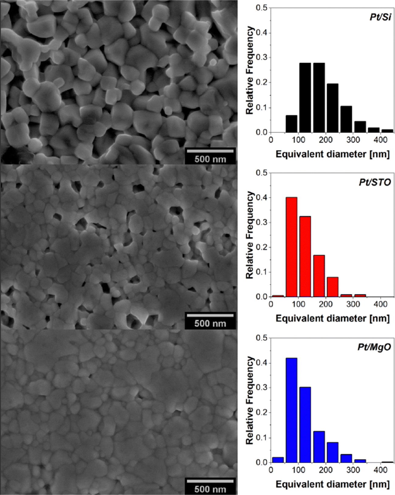 | ||
| Fig. 1 Secondary electron SEM micrographs of KNN thin films on Pt/Si, Pt/STO, Pt/MgO and corresponding grain size distribution. KNN films on Pt/MgO present the most dense and homogeneous microstructure, with small grains and a narrow grain size distribution. | ||
High angular annular dark field (HAADF) STEM micrographs of cross-sectional lamellae of KNN films deposited on Pt/Si, Pt/STO and Pt/MgO substrates also revealed that the films have a polycrystalline microstructure (Fig. 2). Furthermore, KNN films on Pt/Si show a thinner and more irregular thickness as compared to the ones on Pt/STO and Pt/MgO. Using ImageJ and measuring 20 random points across each film, KNN film thickness was estimated to be 352 ± 11 nm, 389 ± 2 nm and 400 ± 5 nm for films deposited on Pt/Si, Pt/STO and Pt/MgO, respectively. Moreover, KNN films on Pt/Si exhibit large grains that cross the entire thickness of the film, while the KNN films on Pt/STO and Pt/MgO exhibit a multi-grain profile across the film thickness. At the same time, the microstructure of KNN films on Pt/STO and Pt/MgO is quite dense and uniform.
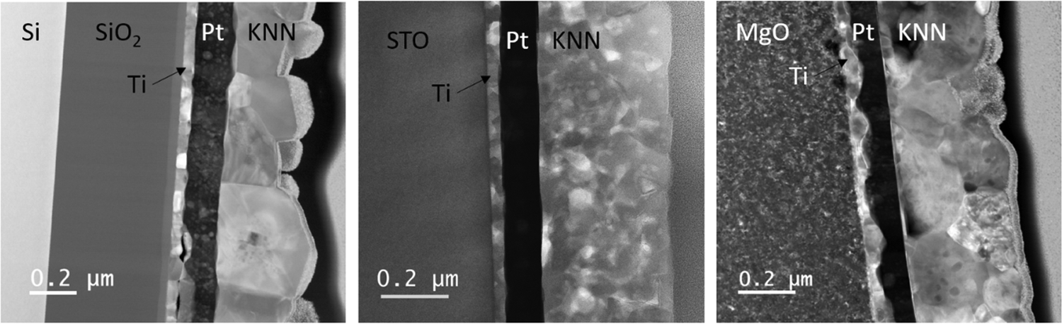 | ||
| Fig. 2 HAADF STEM micrographs of KNN films on Pt/Si (left), Pt/STO (centre) and Pt/MgO (right). Film thickness varies between 350 and 400 nm. Large grains cross the entire thickness of KNN films on Pt/Si, while KNN films on Pt/STO and Pt/MgO present a multi-grain profile across the film thickness. | ||
b. Crystallographic and stress state characterization
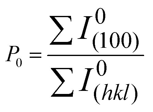
Representative in-plane XRD patterns of KNN films deposited onto Pt/Si, Pt/STO and Pt/MgO substrates are illustrated in Fig. 3. The XRD patterns reveal well crystallized KNN films with the expected K0.507Na0.502NbO3 perovskite structure, regardless of the used substrate. No spurious phases were detected within the sensitivity limit of the technique. The intensity of the (100) peak is similar to that of the (111) peak, whereas, according to PDF #00-065-0275, the (111) peak should exhibit the highest intensity. The observed (100) peak intensity increase is commonly reported for KNN films, with preferential growth along the (100) pseudocubic crystallographic direction.13,16,21,27 The Lotgering factor,25f, was used to estimate the crystallographic texture of the films as: | (1) |
 | (2) |
 | (3) |
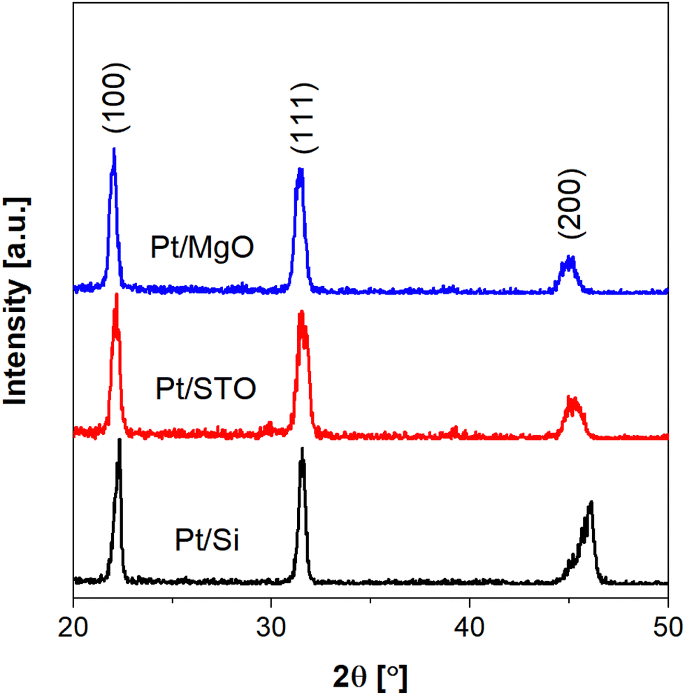 | ||
| Fig. 3 X-ray diffraction patterns of KNN thin films on Pt/Si, Pt/STO and Pt/MgO substrates. KNN peaks are marked by the corresponding pseudocubic indexes, following the Powder Diffraction File of K0.507Na0.502NbO3 (PDF# 00-065-0275). Well crystallized KNN perovskite type structure films were obtained regardless of the used substrate. | ||
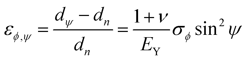
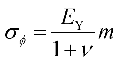
Residual stresses were calculated using the XRD sin2ψ method.28 Lattice spacing, d, values of the (111) planes were determined at different tilt angles ψ (inclined exposure). The strain was calculated from the angular shift of the (111) reflections, as a function of the tilt angle, and the corresponding film residual stress was calculated by using the following equation:
 | (4) |
 | (5) |
ψ, as presented in Fig. 4. The slopes of the linear fits for the KNN films deposited onto the different substrates are given in Fig. 4. While a positive slope is obtained for the KNN films deposited onto Pt/Si, giving evidence for a tensile residual stress state, negative slopes are obtained for the KNN films on Pt/STO and Pt/MgO, evidencing a compressive residual stress state; the larger one was observed for the KNN films on Pt/MgO substrates. The calculated residual stress values are 210 ± 28 MPa, −411 ± 18 MPa and −494 ± 26 MPa for KNN films deposited onto Pt/Si, Pt/STO and Pt/MgO, respectively.
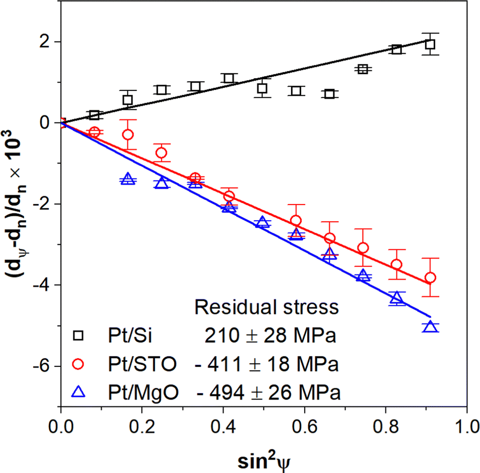 | ||
| Fig. 4 Normalized lattice spacing of KNN thin films on Pt/Si (black squares), Pt/STO (red circles) and Pt/MgO (blue triangles), as a function of sin2ψ. A tensile residual stress state characterizes KNN films on Pt/Si with positive variation slope (black line), while KNN films on Pt/STO and Pt/MgO exhibit a compressive residual stress condition with negative variation slopes (red and blue lines, respectively). | ||
c. Dielectric, ferroelectric and piezoelectric properties under room conditions
Fig. 5 presents the room temperature relative dielectric permittivity and dielectric losses as a function of frequency of the studied films for the 100 Hz–1 MHz frequency range. The frequency dependence of both permittivity and losses is rather similar for the KNN films deposited on Pt/Si and Pt/STO. No hint of dielectric relaxation process in this frequency range could be ascertained. The electric permittivity at 1 kHz is ∼225 for KNN films on Pt/Si and Pt/STO and 250 for KNN films on Pt/MgO. These values are close to the reported range for KNN bulk and single crystal ceramics, which can vary between ∼30030 and ∼700.28,31 Among the studied films, KNN films on Pt/MgO substrates exhibited the lowest dielectric losses, while keeping the highest relative dielectric permittivity above 300 Hz, with the smaller variation within the scanned frequency range. The rather small dielectric losses suggest a more insulating nature as compared with the other two substrates.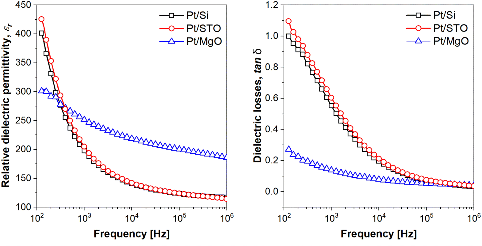 | ||
| Fig. 5 Room temperature relative dielectric permittivity (right) and dielectric loss (left) as a function of frequency for KNN films on Pt/Si, Pt/STO and Pt/MgO substrates. KNN films on Pt/MgO exhibit the lowest dielectric losses with the highest permittivity above 300 Hz. | ||
The macroscopic polarization as a function of the applied ac electric field (P(E)), as well as the current density versus ac electric field (J(E)), recorded at 50 Hz and room temperature, on KNN films deposited on Pt/Si, Pt/STO and Pt/MgO, is shown in Fig. 6. No saturation of the electric polarization could be achieved. The maximum electric field strength that could be applied to the KNN films deposited on Pt/Si and Pt/STO is quite similar (60 kV cm−1) but it increases to 100 kV cm−1 for the dense KNN films deposited on Pt/MgO, corroborating the low dielectric losses at low frequencies in the latter films. The maximum electric polarization was obtained for the KNN films deposited on Pt/MgO substrates, reaching ∼9 μC cm−2. The P(E) hysteretic curves of KNN films on Pt/Si exhibit the smallest polarization value (∼3 μC cm−2), while the P(E) curve is asymmetric, suggesting the existence of internal fields. The differences between the maximum electric polarization reflect the high electric field sustained by the KNN films deposited on Pt/MgO substrates. The ferroelectric switching in the J(E) curves is obscured by leakage current for the films on all of the three substrates, which is rarely reported but common for undoped KNN thin films at room temperature.32
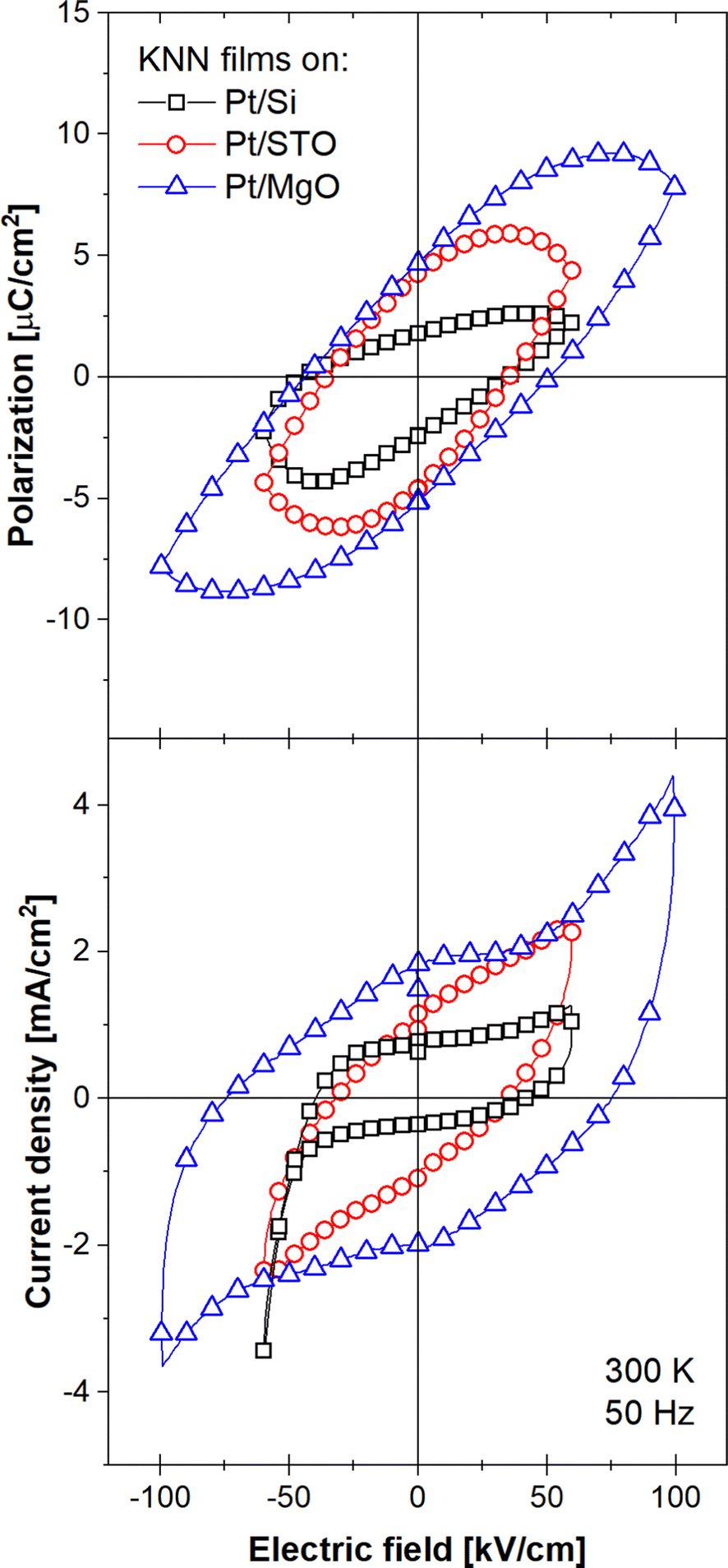 | ||
| Fig. 6 Room temperature polarization P (top) and current density J (bottom) versus electric field E loops for KNN films on Pt/Si, Pt/STO and Pt/MgO substrates at RT, recorded at 50 Hz. KNN films on Pt/MgO exhibit the maximum electric polarization while those on Pt/Si exhibit the smallest polarization. | ||
The local surface roughness was measured by AFM to be about 50 nm for films on Si and MgO substrates and about 30 nm for films on STO (Fig. 7). The film grain distribution corroborates the results of SEM, being denser and homogenous for KNN films on MgO and mostly inhomogeneous for films deposited on Si substrates. Both the local out-of-plane and in-plane PFM signals in KNN films on STO and MgO substrates were successfully measured, while a small out-of-plane PFM signal was acquired for films on Si substrates (Fig. 7). This result can be attributed to the considerable influence of the strain and highlights that the tensile residual stress (the case of Si substrates) almost completely neglects the out-of-plane component of the piezoresponse of these KNN thin films. In contrast, the compressive residual stress (films on STO and MgO substrates) favours the strong appearance of both out-of-plane and in-plane piezoresponses.
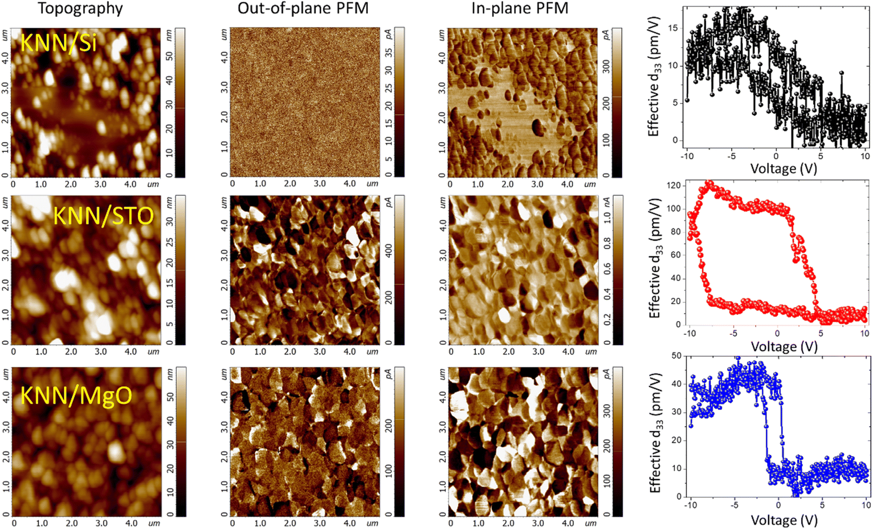 | ||
| Fig. 7 PFM scan images of KNN films on Si, STO and MgO substrates. Tensile residual stress (films on Si) almost completely neglects the out-of-plane component of the piezoresponse in the thin films of KNN. | ||
Local piezoelectric loops were acquired via switching spectroscopy PFM (SS-PFM) at the points possessing the maximum out-of-plane PFM signal. The tensile residual stress dramatically affects the local hysteresis loop measured in KNN films on Si substrates, revealing a small local piezoelectric coefficient of about 15 pm V−1 and a high coercive field (±2 MV cm−1, which corresponds to ±5 V applied to the tip of the probe with an apex radius of about 25 nm). Upon comparing the response of films on STO and MgO substrates, the local piezoresponse demonstrates that stronger compressive residual stress (films on MgO substrates) leads to uniphase out-of-plane domain formation. The piezoresponse signal measured in KNN films on STO produced high-contrast scan images from both the out-of-plane and in-plane components (Fig. 7). This domain configuration is due to a less dense and less stressed grain structure that results in a more open local hysteresis loop with a high local piezoelectric coefficient (∼120 pm V−1) and high coercive field (about −3 MV cm−1 and +2 MV cm−1, which correspond to −7 V and +5 V applied to the tip of the probe with an apex radius of about 25 nm). Comparatively, the local hysteresis loop measured in denser KNN films on MgO substrates has a slimmer shape and a local piezoelectric coefficient of about 50 pm V−1 with a very small coercive field (±0.8 MV cm−1, which corresponds to ±2 V applied to the tip of the probe with an apex radius of about 25 nm). Therefore, the softest switching behaviour is observed in the KNN films on MgO substrates. Thus, the room temperature analysis using AFM, PFM, and SS-PFM clearly demonstrates the significant influence of the substrate on the stress state and microstructure development on the local piezoelectric properties of KNN sol–gel thin films, in accordance with the macroscopic measurements.
d. Structural phase transitions and residual strain effect
To characterize the structural phase transitions, the Raman spectra of KNN films deposited on Pt/Si, Pt/STO and Pt/MgO substrates were recorded at several fixed temperatures. The spectra are shown in Fig. 8 for selected temperatures, corresponding to the cubic, tetragonal and orthorhombic crystallographic phases exhibited by KNN on cooling toward RT. Typical vibrations of KNN phases, similar to those reported for bulk KNN ceramics,31 were observed. At room temperature, KNN has an orthorhombic Amm2 symmetry and theoretical group analysis indicated that KNN has a total of 12 Raman active modes (4A1 + 4B1 + 3B2 + A2).22,33–35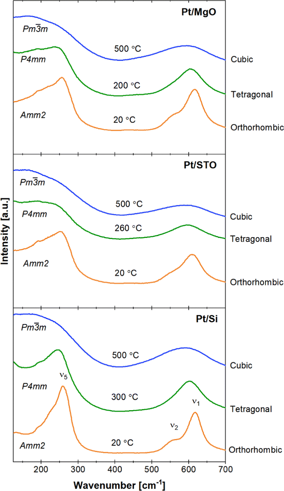 | ||
| Fig. 8 Unpolarized Raman spectra of the orthorhombic, tetragonal, and cubic crystallographic KNN phases of KNN films on Pt/Si, Pt/STO and Pt/MgO substrates, with typical vibrations of the KNN phases. Indications of respective space groups for each temperature were taken from powder diffraction files (PDF card 00-065-0275, 00-065-0276 and 00-065-0277). | ||
Like the potassium niobate and sodium niobate phases, all the peaks below 200 cm−1 represent translational modes of Na+/K+ cations and rotations of the NbO6 octahedra. At room temperature, all KNN films show two strong peaks at ∼260 cm−1 and ∼610 cm−1 and a shoulder at ∼550 cm−1, within the presented range. These peaks can be assigned to ν5, ν1 and ν2 modes, respectively.34 Of these, ν1 and ν2 are stretching modes while ν5 is a bending one. The ν1 vibrational mode weakens and broadens above the Curie temperature (TC, temperature of transition between tetragonal and cubic phase), when ν2 completely disappears. Raman activity in the cubic phase is forbidden, yet these features are common to the cubic phase of ferroelectrics due to local static and/or dynamic disorder reminiscent of the distortions in ferroelectric phases,31,36 and the effect of symmetry breaking at the grain boundaries.31 The orthorhombic to tetragonal phase transition is identified by the disappearance and frequency shifts of vibrational modes. The observed changes in the Raman spectra were found to be universal in the KNN system, including bulk ceramics.31,33–38
The temperature dependencies of the wavelength of selected Raman modes are displayed in Fig. 9. At room temperature, six vibrational modes are present. The three major vibrational modes, ν1 (∼615 cm−1), ν2 (∼555 cm−1) and ν5 (∼260 cm−1), are visible for all KNN films. Particularly, ν1 (∼615 cm−1) and ν5 (∼260 cm−1) have a relatively strong intensity and are detected within the whole measured temperature range. The transition from cubic to tetragonal phase at TC is marked by the appearance of new vibrational modes due to symmetry reduction. The transition from the tetragonal to orthorhombic phase at TO–T is identified by the appearance of a vibrational mode close to ν5 and frequency shifts in the vibrational modes. By mapping the appearance of new modes, the TC values were estimated as 360 °C, 320 °C and 220 °C for KNN films deposited on Pt/Si, Pt/STO and Pt/MgO, respectively. On the other hand, TO–T values were estimated to be 220 °C, 200 °C and 120 °C for KNN films on Pt/Si, Pt/STO and Pt/MgO, respectively, as well.
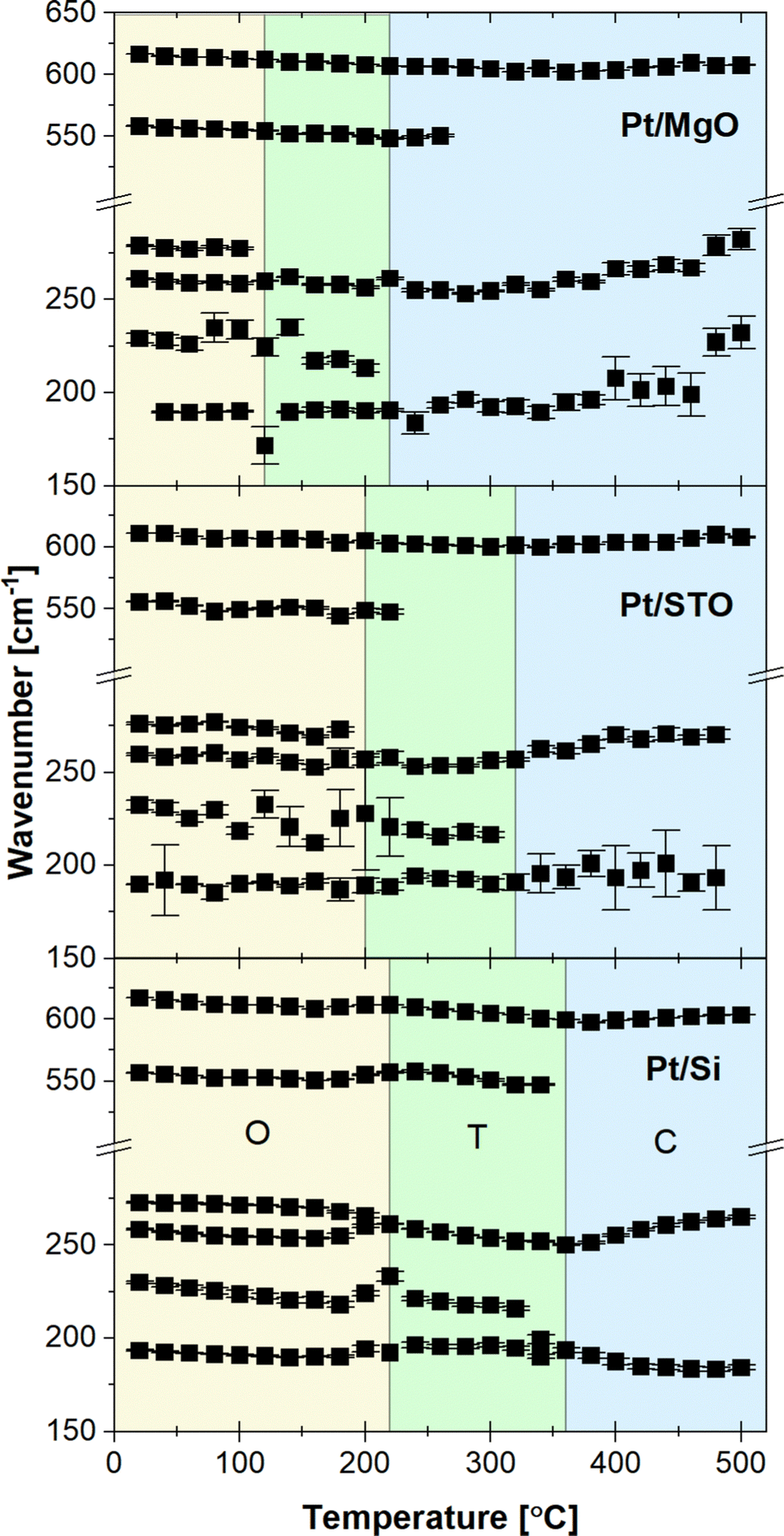 | ||
| Fig. 9 Temperature dependence of the Raman vibrational modes in KNN thin films on Pt/Si, Pt/STO and Pt/MgO substrates. Data in the orthorhombic (O), tetragonal (T) and cubic (C) phases are shown in the yellow, green and blue areas, correspondingly. TC values were estimated as 360 °C, 320 °C and 220 °C for KNN films on Pt/Si, Pt/STO and Pt/MgO, and TO–T values were estimated to be 220 °C, 200 °C and 120 °C for KNN films on Pt/Si, Pt/STO and Pt/MgO, respectively. | ||
Discussion
Table 1 summarizes the results of the characterization of sol–gel derived KNN thin films deposited on Pt/Si, Pt/STO and Pt/MgO substrates, including the structural, microstructural and electric performance data obtained in this work.| Properties of films on platinized substrates | Pt/Si | Pt/STO | Pt/MgO | |
|---|---|---|---|---|
| Residual stress (MPa) | Tensile | Compressive | Compressive | |
| 210 ± 28 | −411 ± 18 | −494 ± 26 | ||
| T O–T (°C) | 220 | 200 | 120 | |
| T C (°C) | 360 | 320 | 220 | |
| Vibrational Raman modes (cm−1) [RT] | ν 1 | 617 | 611 | 616 |
| ν 2 | 557 | 556 | 558 | |
| ν 5 | 258 | 260 | 261 | |
| Average grain size (nm) | 230 ± 5 | 148 ± 4 | 149 ± 4 | |
| Thickness (nm) | 352 ± 11 | 389 ± 2 | 400 ± 5 | |
| Relative dielectric permittivity, εr [RT, 10 kHz] | 141 | 142 | 219 | |
| Dielectric loss, tanδ [RT, 10 kHz] |
0.20 | 0.21 | 0.08 | |
| Coercive field, Ec (kV cm−1) | 36 | 36 | 50 | |
| Remnant polarization, Pr (μC cm−2) | 1.78 | 4.28 | 4.69 | |
| (Local) Piezoelectric coefficient, d33,eff. (pm V−1) | 15 | 120 | 50 | |
As can be seen from the X-ray diffraction patterns, the KNN thin films deposited on different substrates have rather similar crystal structures but significantly different residual stresses. In films, residual stresses may arise from phase transitions, lattice mismatches and thermal expansion misfits between the film and the substrate.39,40 Due to the polycrystalline nature of these films and their random crystal structure orientation, the stress due to phase transitions is not relevant. In addition, as our films are not epitaxial and are deposited on platinized substrates, the possibility of residual stresses arising from lattice mismatch seems not significant as well. Therefore, we assume that the residual stresses measured in the KNN films result from differences between the coefficients of thermal expansion (CTEs) of the materials. The CTE for the substrates (Si = 2.3 × 10⁻⁶ K−1, STO = 10.4 × 10⁻⁶ K−1, MgO = 12.8 × 10⁻⁶ K−1) and KNN (KNNO = 2.96 × 10⁻⁶ K−1, KNNT = 4.35 × 10⁻⁶ K−1 and KNNC = 7.72 × 10⁻⁶ K−1) films follow the order Si < KNN < SrTiO3 < MgO (Fig. 10; data from supplier for Si, STO and MgO substrates; and from reference41 for KNN), which should result in tensile stress for KNN films on Si and compressive stresses in KNN films on STO and MgO.
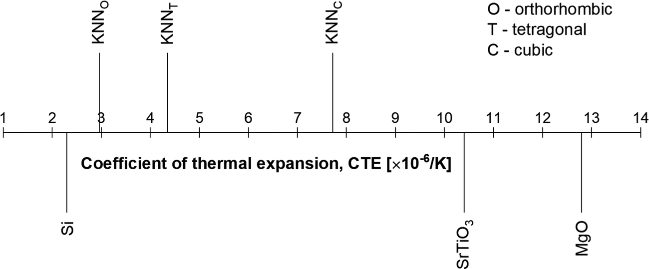 | ||
| Fig. 10 Coefficients of thermal expansion (CTEs) for the substrates (Si, SrTiO3 and MgO) and KNN phases (orthorhombic, tetragonal, and cubic). The data were collected from the supplier and from ref. 41. | ||
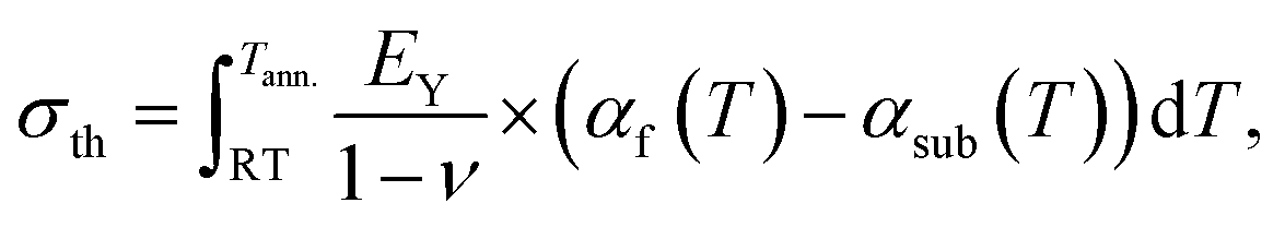
The residual stress due to the misfit of CTE was calculated theoretically using the following equation:24
 | (6) |
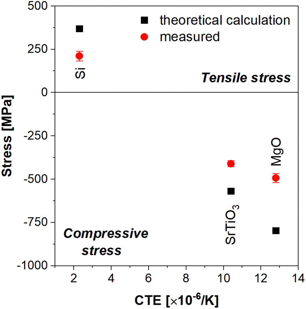 | ||
| Fig. 11 Residual stress (red circles) and theoretical stress calculation of thermal stress (black squares) for KNN films on Pt/Si, Pt/STO and Pt/MgO substrates. The residual stress follows the trend exhibited by the calculated thermal stresses. | ||
Characteristic Raman spectra of orthorhombic Amm2 symmetry were observed at room temperature, which agrees with the X-ray diffraction analysis on the KNN structure at RT. By following the structure evolution of KNN films via Raman spectroscopy, it can be observed that both the transition between orthorhombic and tetragonal phases and the transition between tetragonal and cubic phases occur at significantly different temperatures, TO–T and TC, respectively, with the lowest for KNN films on Pt/MgO and the highest for KNN films on Pt/Si. These observations are supported by preliminary dielectric permittivity and dielectric loss variations with the temperature of these films (not shown). Not only are the phase transitions reduced proportionally to the magnitude of residual stress, but the stability of the tetragonal phase is considerably reduced (∼30%) from 140 °C temperature range for KNN films on Pt/Si, to 100 °C range for KNN films on Pt/MgO (Fig. 12). Despite some uncertainty in the definition of the phase transition temperatures, they do not overlap each other, which means that the phase transitions shift as a function of the used substrate. Due to the polycrystalline nature of these KNN films, we hypothesize that a shift of the phase transition to lower temperatures could be related to quasi-hydrostatic residual stresses, similar to that of bulk polycrystalline KNN ceramics, where both tensile and compressive stresses result in a reduction of the transition temperatures.28 Therefore, the transition temperature would be dependent on the magnitude of residual stresses, i.e., the residual stress for KNN films on Pt/MgO is higher than the residual stress of KNN films on Pt/STO and Pt/Si, which resulted in a lower phase transition temperature. The residual stress for KNN films on Pt/Si is the lowest in magnitude and these KNN films present the highest transition temperatures (Fig. 12). These results point, for the first time, to the possibility of generating a morphotropic phase boundary in KNN thin films under compressive residual stress.
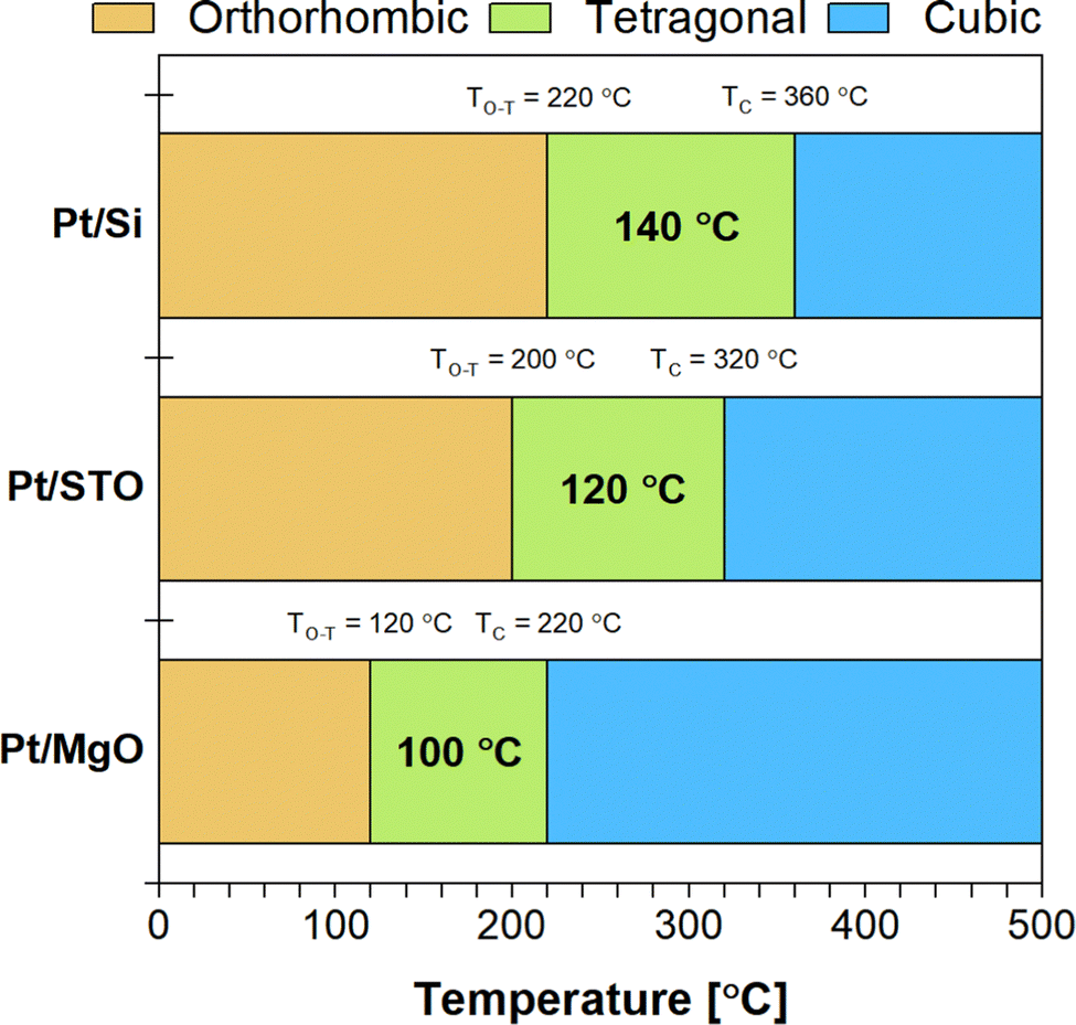 | ||
| Fig. 12 Schematic representation of the evolution of the phase transitions in KNN films deposited on Pt/Si, Pt/STO and Pt/MgO, with highlighted temperature ranges of tetragonal phase stability. KNN thin films on MgO present the lowest temperature range for tetragonal phase. | ||
Despite all the KNN films were submitted to the same thermal cycle, a significant difference can be observed in the final grain size distribution and average grain size values, particularly between KNN films deposited on Pt/Si (230 ± 5 nm) and those deposited on Pt/STO (148 ± 4 nm) or Pt/MgO (149 ± 4 nm). Correspondingly, a significant difference in the microstructure arises between the films on silicon and on the two oxide substrates (STO and MgO). We hypothesize that the differences observed in the microstructure could be related to the about one order of magnitude difference in thermal conductivity of Si of 130 W (m K)−1 and of STO of 12 W (m K)−1 and MgO of 42 W (m K)−1 [values obtained from the supplier]. Under a very rapid thermal treatment such as the RTA used in this work, such differences will play a role in the film heating process. As the thermal conductivity decreases, heat dissipation is reduced, leading to higher local temperatures in the films. The higher the temperature in the film, the more thermal energy available for nucleation, which could later result in a small average grain size.43 In our case, the lower thermal conductivity of the STO and MgO substrates might result in higher temperatures in the KNN films during the annealing process, which could be related to a higher nucleation energy resulting in smaller average grain sizes compared with KNN films prepared on silicon substrates.
The dielectric and ferroelectric response of KNN films can be influenced by stress, grain size distribution, porosity, impurities, crystallographic texture, and oxygen vacancy concentration, among other factors.24 Besides stress, particle size distribution and porosity, the other causes contributing to this variation should be similar in this study since the KNN films were all processed with exactly the same method. Table 1 highlights that sol–gel derived KNN thin films on Pt/Si have the largest grain size but are also the most porous, exhibiting the lowest dielectric permittivity. In contrast, the highest dielectric permittivity and the lowest losses observed in this work seem to be associated with the lowest apparent porosity observed in KNN films on Pt/MgO. Tkach et al.23 reported similar values of room temperature relative dielectric permittivity, with values ranging between 75 and 275 for films deposited on platinized Si and STO substrates. The minimum dielectric loss was reported to reach 10% in value and its frequency was substrate-dependent, where for Pt/Si substrates it occurs in the frequency range of 103 to 104 Hz and for Pt/STO it occurs at around 105 Hz. The dielectric permittivity values obtained in our work are quite similar, yet our dielectric losses seem to present a more stable behaviour.
On the other hand, stress/strain influences the ferroelectric response. The compressive stress imposed by the Pt/MgO substrates, developed during the cooling from crystallization temperature to RT, could direct the favourable Nb5+ ionic motion from in-plane towards out-of-plane, resulting in an increase of the polarization measured along this direction. For KNN films on Pt/STO, the residual stress of −411 ± 18 MPa is smaller than that of −494 ± 26 MPa for the films on Pt/MgO corresponding to a decrease in the polarization. In contrast, KNN films on Pt/Si present tensile stresses, which might result in reduced out-of-plane Nb5+ ionic motion in favour of the in-plane one, explaining the smallest polarization measured along the out-of-plane direction.
When comparing with previous data on undoped KNN films reported mainly on Si substrates (Table 2), it is clear that they range quite widely from a remnant polarization of 2.65 μC cm−2 for sol–gel derived KNN films, crystallized at 750 °C, on Pt/Si23 to that of 22.5 μC cm−2 for rf magnetron sputtered KNN films on the same substrates.44 Coercive field varies from 35 kV cm−1 for sol–gel derived KNN films with a 20% initial alkali excess13 to ∼100 kV cm−145 for pulsed laser deposited KNN. Moreover, the effective d33 piezoelectric coefficient ranged from 37 pm V−1 for KNN films sputtered on Si with a Ni electrode46 to 80 pm V−1 for (001)-oriented KNN thin films grown by pulsed laser deposition on Pt(111)/TiO2/SiO2/Si substrates with further treatment in O2 plasma and vacuum annealing.45 In addition, for sol–gel derived Mn-doped KNN films on Nb:STO substrates with different crystallographic orientations ((100), (110) and (111)),17 the macroscopic P–E curves were collected at 100 Hz and a maximum field of 400 kV cm−1 was used for the Mn-KNN films on (100) and (110) oriented Nb:STO substrates, while 700 kV cm−1 was used for the Mn-KNN films on the (111)-Nb:STO ones. Remnant polarizations of 9 μC cm−2, 17.3 μC cm−2 and 8 μC cm−2, and coercive fields of 115 kV cm−1, 105 kV cm−1 and 75 kV cm−1, were reported for Mn-KNN films deposited on (100), (110) and (111) Nb:ST substrates, respectively. Highly oriented sol–gel derived KNN films on (100)Pt/MgO substrates presented P–E hysteresis loops measured at 1 kHz, −190 °C, with a maximum field of 350 kV cm−1, achieving a remnant polarization of 20.5 μC cm−2 and coercive field of 45 kV cm−1.47 The Pr values of our KNN sol–gel derived thin films are within the values descibed in the literature, despite the wide range of conditions, as shown in Table 2.
| KNN sol–gel films on: | Freq. [Hz] | Max. applied field [kV cm−1] | P r [μC cm−2] | E c [kV cm−1] | d 33 [pm V−1] | Ref. |
|---|---|---|---|---|---|---|
| Pt/STO | 50 | 75 | 4.56 | ∼40 | — | 23 |
| Pt/TiO2/SiO2/Si | 50 | 75 | 2.65 | ∼40 | — | 23 |
| Pt/TiO2/SiO2/Si | — | 500 | 22.5 | 90 | 45 | 44 |
| Pt/Ti/SiO2/Si | — | 400 | ∼3 | ∼50 | 74 | 48 |
| Pt/Ti/SiO2/Si | — | 600 | 16.4 | 42 | 61 | 49 |
| Pt(111)/TiO2/SiO2/Si | 1000 | 500 | 12.6 | ∼100 | 58 | 45 |
| Pt/TiOx/SiO2/Si | 1000 | 500 | 7 | 70 | 46 | 50 |
| Pt(111)/Ti/SiO2/Si(100) | 130 | 200 | 10 | 35 | 40 | 13 |
| Pt(111)/Ti/SiO2/Si | 100–2000 | 100 | 2.5 | ∼60 | 80 | 51 |
| Ni/Ti/SiO2/Si | 20000 |
100 | 12 | 35 | 37 | 46 |
| LaNiO3/Si | — | 200 | 12 | 48 | 58 | 52 |
| Pt/Si | 50 | 60 | 1.78 | 36 | 15 | This work |
| Pt/STO | 50 | 60 | 4.28 | 36 | 120 | This work |
| Pt/MgO | 50 | 100 | 4.69 | 50 | 50 | This work |
Conclusions
Polycrystalline KNN thin films were synthesised, using a sol–gel method, and spin-coated on Pt/Si, Pt/STO and Pt/MgO substrates under the same processing conditions. Regardless of the several layers that compose the substrates, it was found that the main substrate material (i.e., Si, STO and MgO) controls the thermal stress effect on the KNN films. According to XRD data, KNN films on Pt/Si present tensile residual stresses while KNN films on Pt/STO and Pt/MgO exhibit compressive stresses. The biaxial nature of the compressive stresses induced by Pt/MgO results in enhanced out-of-plane remnant polarization. Additionally, the low porosity of these films has a positive impact on the relatively high dielectric permittivity and low dielectric losses. The differences in the microstructure of the films deposited on different substrates were attributed to variations in the thermal conductivities of the substrates. The residual stresses markedly change the phase transition temperatures. TC values of 360 °C, 320 °C and 220 °C, as well as TO–T values of 220 °C, 200 °C and 120 °C, were determined using in-situ Raman spectroscopy of the KNN films deposited on Pt/Si, Pt/STO and Pt/MgO, respectively. Not only are the phase transitions reduced as a function of the magnitude of residual stresses, but also the stability of the tetragonal phase is reduced. These results suggest, for the first time, the possibility of generating the morphotropic phase boundary in KNN thin films under compressive residual stress.In conclusion, we have reported a systematic study on how mechanical stress impacts the dielectric, polar and structural properties of KNN polycrystalline thin films at the nano-, micro-, and macroscale levels. These observations provide insight into a previously unknown aspect of the manner by which distortions may tune electrical performance of KNN polycrystalline films. Now we understand and have shown how the ferroelectric/piezoelectric performance can be enhanced by stress/strain level control in KNN thin films, via the proper choice of substrates. The combination of a low-cost process, i.e. the sol–gel methodology, and commercially available substrates suggests KNN thin film applications as sensors or piezoelectric harvesters.
Conflicts of interest
There are no conflicts to declare.Acknowledgements
This work was developed within the scope of the project CICECO – Aveiro Institute of Materials, UIDB/50011/2020, UIDP/50011/2020 & LA/P/0006/2020; FLEXIDEVICE project PTDC/CTMCTM/29671/2017, and through IDMEC, under LAETA, UIDB/50022/2020, financed by national funds through the FCT/MEC (PIDDAC). Rui Vilarinho and J. Agostinho Moreira acknowledge FCT for financial support, under the projects PTDC/NAN-MAT/0098/2020, UIDB/04968/2021 and UIDP/04968/2021. Rui Pinho, Fátima Zorro and Alexander Tkach acknowledge FCT for financial support, under the studentships SFRH/BD/12069/2016, 2021.05950.BD, and individual FCT grant 2021.02284.CEECIND, respectively.References
- D. Damjanovic and G. A. Rossetti, Strain generation and energy-conversion mechanisms in lead-based and lead-free piezoceramics, MRS Bull., 2018, 43(8), 588–594 CrossRef CAS.
- European Commission, Directive 2011/65/EU of the European Parliament and the Council of 8 June 2011 - ROHS, Off. J. Eur. Union, 2011, 54(1), 88–110 Search PubMed.
- M. Ahtee and A. W. Hewat, Structural phase transitions in sodium–potassium niobate solid solutions by neutron powder diffraction, Acta Crystallogr., Sect. A: Cryst. Phys., Diffr., Theor. Gen. Crystallogr., 1978, 34(2), 309–317 CrossRef.
- Y. Saito, et al., Lead-free piezoceramics, Nature, 2004, 432, 84–87 CrossRef CAS PubMed.
- J. F. Li, K. Wang, F. Y. Zhu, L. Q. Cheng and F. Z. Yao, (K, Na)NbO3-based lead-free piezoceramics: Fundamental aspects, processing technologies, and remaining challenges, J. Am. Ceram. Soc., 2013, 96(12), 3677–3696 CrossRef CAS.
- M. A. Rafiq, M. E. Costa, A. Tkach and P. M. Vilarinho, Impedance analysis and conduction mechanisms of lead free potassium sodium niobate (KNN) single crystals and polycrystals: A comparison study, Cryst. Growth Des., 2015, 15(3), 1289–1294 CrossRef CAS.
- M. A. Rafiq, M. N. Rafiq, F. Ahmed, L. Ali and M. Y. Anwar, Structure, Dielectric and Impedance Studies of Li Doped (K0.5Na0.5)NbO3 Ceramics, J. Fac. Eng. Technol., 2014, 21(1), 167–178 Search PubMed.
- G. H. Haertling, Ferroelectric thin films for electronic applications, J. Vac. Sci. Technol., A, 1991, 9(3), 414–420 CrossRef CAS.
- G. H. Haertling, Ferroelectric Ceramics: History and Technology, J. Am. Ceram. Soc., 1999, 82(4), 797–818 CrossRef CAS.
- K. Uchino, Glory of piezoelectric perovskites, Sci. Technol. Adv. Mater., 2015, 16(4), 46001 CrossRef PubMed.
- J. Rödel, K. G. Webber, R. Dittmer, W. Jo, M. Kimura and D. Damjanovic, Transferring lead-free piezoelectric ceramics into application, J. Eur. Ceram. Soc., 2015, 35(6), 1659–1681 CrossRef.
- K. Tanaka, H. Hayashi, K. I. Kakimoto, H. Ohsato and T. Iijima, Effect of (Na,K)-excess precursor solutions on alkoxy-derived (Na,K)NbO3 powders and thin films, Jpn. J. Appl. Phys., Part 1, 2007, 46(10B), 6964–6970 CrossRef CAS.
- C. W. Ahn, et al., The effect of K and Na excess on the ferroelectric and piezoelectric properties of K0.5Na0.5NbO3 thin films, J. Phys. D: Appl. Phys., 2009, 42(21), 215304 CrossRef.
- X. Yan, W. Ren, X. Wu, P. Shi and X. Yao, Lead-free (K, Na)NbO3 ferroelectric thin films: Preparation, structure and electrical properties, J. Alloys Compd., 2010, 508(1), 129–132 CrossRef CAS.
- J.-H. Park, C. Kang, D.-J. Kim, D. Shen, H. Ahn and M. Park, Growth and characterization of (K0.5Na0.5)NbO3 thin films by a sol–gel method, J. Sol–Gel Sci. Technol., 2010, 58(1), 85–90 Search PubMed.
- A. Kupec, B. Malic, J. Tellier, E. Tchernychova, S. Glinsek and M. Kosec, Lead-free ferroelectric potassium sodium niobate thin films from solution: Composition and structure, J. Am. Ceram. Soc., 2012, 95(2), 515–523 CrossRef CAS.
- Q. Yu, et al., Electrical properties of K0.5Na0.5NbO3 thin films grown on Nb:SrTiO3 single-crystalline substrates with different crystallographic orientations, J. Appl. Phys., 2013, 113, 024101 CrossRef.
- X. Vendrell, et al., Effect of lanthanide doping on structural, microstructural and functional properties of K0.5Na0.5NbO3 lead-free piezoceramics, Ceram. Int., 2016, 42(15), 17530–17538 CrossRef CAS.
- Q. Deng, et al., Optoelectronic properties and polar nano-domain behavior of sol–gel derived K0.5Na0.5Nb1−xMnxO3−δ nanocrystalline films with enhanced ferroelectricity, J. Mater. Chem. C, 2015, 3(31), 8225–8234 RSC.
- S. S. Won, et al., Lead-free Mn-doped (K0.5Na0.5)NbO3 piezoelectric thin films for MEMS-based vibrational energy harvester applications, Appl. Phys. Lett., 2016, 108, 232908 CrossRef.
- C.-M. Weng, et al., Effects of Non-Stoichiometry on the Microstructure, Oxygen Vacancies, and Electrical Properties of KNN-Based Thin Films, ECS J. Solid State Sci. Technol., 2016, 5(9), N49–N56 CrossRef CAS.
- C. W. Ahn, et al., Raman spectra study of K0.5Na0.5NbO3 ferroelectric thin films, Jpn. J. Appl. Phys., 2010, 49, 095801 CrossRef.
- A. Tkach et al., Strain Effect on the Properties of Polar Dielectric Thin Films, in Advances in Thin Films, Nanostructured Materials and Coatings, ed. A. Pogrebnjak and V. Novosad, Springer, Singapore, 2019 Search PubMed.
- A. Tkach, O. Okhay, I. M. Reaney and P. M. Vilarinho, Mechanical strain engineering of dielectric tunability in polycrystalline SrTiO3 thin films, J. Mater. Chem. C, 2018, 6, 2467–2475 RSC.
- C. K. Jeong, et al., Flexible highly-effective energy harvester via crystallographic and computational control of nanointerfacial morphotropic piezoelectric thin film, Nano Res., 2017, 10(2), 437–455 CrossRef CAS.
- E. Soergel, Piezoresponse force microscopy (PFM), J. Phys. D: Appl. Phys., 2011, 44, 464003 CrossRef.
- A. Tkach, et al., Strain-mediated substrate effect on the dielectric and ferroelectric response of potassium sodium niobate thin films, Coatings, 2018, 8, 449 CrossRef.
- R. Pinho, et al., Spark plasma texturing: A strategy to enhance the electro-mechanical properties of lead-free potassium sodium niobate ceramics, Appl. Mater. Today, 2020, 19, 100566 CrossRef.
- R. Pinho, A. Tkach, M. A. Carpenter, J. Noudem, M. E. Costa and P. M. Vilarinho, Elastic moduli of potassium sodium niobate ceramics: Impact of spark plasma texturing, Scr. Mater., 2022, 218, 114837 CrossRef CAS.
- M. A. Rafiq, M. E. Costa and P. M. Vilarinho, Establishing the domain structure of (K0.5Na0.5)NbO3 (KNN) single crystals by piezoforce-response microscopy, Sci. Adv. Mater., 2014, 6(3), 426–433 CrossRef CAS.
- M. M. Gomes, et al., Revisiting the phase sequence and properties of K0.5Na0.5NbO3 ceramics sintered by different processes, Ceram. Int., 2021, 47(6), 8308–8314 CrossRef CAS.
- N. H. Gaukås, J. Glaum, M. A. Einarsrud and T. Grande, Ferroelectric and dielectric properties of Ca2+-doped and Ca2+-Ti4+ co-doped K0.5Na0.5NbO3 thin films, J. Mater. Chem. C, 2020, 8(15), 5102–5111 RSC.
- R. Singh, K. Kambale, A. R. Kulkarni and C. S. Harendranath, Structure composition correlation in KNN-BT ceramics-An X-ray diffraction and Raman spectroscopic investigation, Mater. Chem. Phys., 2013, 138(2–3), 905–908 CrossRef CAS.
- K. I. Kakimoto, K. Akao, Y. Guo and H. Ohsato, Raman scattering study of piezoelectric (Na0.5K0.5)NbO3-LiNbO3 ceramics, Jpn. J. Appl. Phys., Part 1, 2005, 44(9B), 7064–7067 CrossRef CAS.
- M. Polomska, B. Hilczer, M. Kosec and B. Malič, Raman scattering studies of lead free (1-x)K0.5Na0.5NbO3-xSrTiO3 relaxors, Ferroelectrics, 2008, 369(1 PART 3), 149–156 CrossRef CAS.
- H. J. Trodahl, et al., Raman spectroscopy of (K,Na)NbO3 and (K,Na)1−xLixNbO3, Appl. Phys. Lett., 2008, 93, 262901 CrossRef.
- B. Malic, M. Kosec, E. Buixaderas, I. Gregora, D. Nuzhnyy and S. Kamba, Polar Modes in K0.5Na0.5NbO3 Ceramics, Ferroelectrics, 2009, 391(1), 51–57 CrossRef.
- N. Klein, E. Hollenstein, D. Damjanovic, H. J. Trodahl, N. Setter and M. Kuball, A study of the phase diagram of (K,Na,Li)NbO3 determined by dielectric and piezoelectric measurements, and Raman spectroscopy, J. Appl. Phys., 2007, 102, 014112 CrossRef.
- T. Ohno, et al., Origin of compressive residual stress in alkoxide derived PbTiO3 thin film on Si wafer, Jpn. J. Appl. Phys., 2008, 47(9 PART 2), 7514–7518 Search PubMed.
- Q. Yu, F.-Y. Zhu, L.-Q. Cheng, K. Wang and J.-F. Li, Determination of crystallographic orientation of lead-free piezoelectric (K,Na)NbO3 epitaxial thin films grown on SrTiO3 (100) surfaces, Appl. Phys. Lett., 2014, 104, 102902 CrossRef.
- B. Malič, H. Razpotnik, J. Koruza, S. Kokalj, J. Cilenšek and M. Kosec, Linear thermal expansion of lead-free piezoelectric K0.5Na 0.5NbO3 ceramics in a wide temperature range, J. Am. Ceram. Soc., 2011, 94(8), 2273–2275 CrossRef.
- R. E. Jaeger and L. Egerton, Hot Pressing of Potassium-Sodium Niobates, J. Am. Ceram. Soc., 1962, 45(5), 209–213 CrossRef CAS.
- R. W. Schwartz, T. Schneller and R. Waser, Chemical solution deposition of electronic oxide films, C. R. Chim., 2004, 7(5), 433–461 CrossRef CAS.
- H. J. Lee, I. W. Kim, J. S. Kim, C. W. Ahn and B. H. Park, Ferroelectric and piezoelectric properties of Na0.52K0.48NbO3 thin films prepared by radio frequency magnetron sputtering, Appl. Phys. Lett., 2009, 94, 092902 CrossRef.
- M. D. Nguyen, M. Dekkers, E. P. Houwman, H. T. Vu, H. N. Vu and G. Rijnders, Lead-free K0.5Na0.5NbO3 thin films by pulsed laser deposition driving MEMS-based piezoelectric cantilevers, Mater. Lett., 2016, 164, 413–416 CrossRef CAS.
- A. Bani Milhim and R. Ben-Mrad, Fabrication of Lead-Free Piezoelectric (K, Na)NbO3 Thin Film on Nickel-Based Electrodes, J. Microelectromechanical Syst., 2016, 25(2), 320–325 Search PubMed.
- Y. Nakashima, W. Sakamoto and T. Yogo, Processing of highly oriented (K, Na)NbO3 thin films using a tailored metal-alkoxide precursor solution, J. Eur. Ceram. Soc., 2011, 31(14), 2497–2503 CrossRef CAS.
- P. C. Goh, K. Yao and Z. Chen, Lead-free piezoelectric (K0.5Na0.5)NbO3 thin films derived from chemical solution modified with stabilizing agents, Appl. Phys. Lett., 2010, 97, 102901 CrossRef.
- L. Wang, K. Yao and W. Ren, Piezoelectric K0.5Na0.5NbO3 thick films derived from polyvinylpyrrolidone-modified chemical solution deposition, Appl. Phys. Lett., 2008, 93, 092903 CrossRef.
- Y. Nakashima, W. Sakamoto, H. Maiwa, T. Shimura and T. Yogo, Lead-Free Piezoelectric (K,Na)NbO3 Thin Films Derived from Metal Alkoxide Precursors, Jpn. J. Appl. Phys., 2007, 46(14), L311–L313 CrossRef CAS.
- C. Groppi, L. Mondonico, F. Maspero, C. Rinaldi, M. Asa and R. Bertacco, Effect of substrate preparation on the growth of lead-free piezoelectric (K0.5Na0.5)NbO3 on Pt(111), J. Appl. Phys., 2021, 129, 194102 CrossRef CAS.
- T. Li, G. Wang, K. Li, N. Sama, D. Remiens and X. Dong, Influence of LNO top electrodes on electrical properties of KNN/LNO thin films prepared by RF magnetron sputtering, J. Am. Ceram. Soc., 2013, 96(3), 787–790 CrossRef CAS.
| This journal is © The Royal Society of Chemistry 2023 |