
Anisotropic X-ray detection performance of melt-grown CsPbBr3 single crystals†
Yunqiu
Hua‡
,
Xue
Sun‡
,
Xiang
Li
,
Fucai
Cui
,
Zhongjie
Yue
,
Jiaxin
Liu
,
Hongjie
Liu
,
Guodong
Zhang
* and
Xutang
Tao
 *
*
State Key Laboratory of Crystal Materials, Institute of Crystal Materials, Shandong University, Jinan 250100, P. R. China. E-mail: zgd@sdu.edu.cn; txt@sdu.edu.cn
First published on 13th June 2023
Abstract
All-inorganic perovskite CsPbBr3 has been regarded as a new semiconductor radiation material with great potential due to its excellent carrier transport performance and thermal stability. However, it remains challenging to optimize the size and quality of CsPbBr3 single crystals for commercial applications. Here, the [100], [010], and [001] orientations of bulk CsPbBr3 single crystals were examined, and their anisotropic X-ray detection performance was investigated. The regular positive and negative charge distributions at the outer (010) surface and the connection of [PbBr6]4− octahedrons with the [010] orientation contribute to decreased defect densities and enhanced carrier transportation of the (010) facet. Additionally, the wafer with the [010] orientation exhibited the weakest ion migration among the three orientations due to the largest active energy (143.77 meV) and ion diffusion barrier energy (0.361 eV), which is advantageous for enhancing the X-ray response. Moreover, the (010) CsPbBr3 single crystal detector, which was fabricated with EGaIn and Au electrons, demonstrated the maximum sensitivity of 34![[thin space (1/6-em)]](https://www.rsc.org/images/entities/char_2009.gif) 449 μC Gyair−1 cm−2 under a high bias voltage of −400 V and the lowest detection limit of 52.6 nGyair s−1 compared with the other two devices. This work highlights the anisotropic engineering of large-size single crystals for boosting perovskite radiation performance and provides valuable advice for the oriented growth of large-size crystals and films.
449 μC Gyair−1 cm−2 under a high bias voltage of −400 V and the lowest detection limit of 52.6 nGyair s−1 compared with the other two devices. This work highlights the anisotropic engineering of large-size single crystals for boosting perovskite radiation performance and provides valuable advice for the oriented growth of large-size crystals and films.
 Guodong Zhang | Guodong Zhang is a full professor at the Institute of Crystal Materials, Shandong University. He received his PhD degree in 2012 under the supervision of Prof. Xutang Tao at Shandong University. From 2013 to 2015, he worked on his postdoctoral research on the solvo-thermal synthesis of novel chalcogenide crystals and liquid-phase epitaxy (LPE) growth of novel nitride single crystals at Nanyang Technological University's Materials Science Division and National Institute for Materials Science, respectively. His current research interest is focused on the growth of metal halide bulk single crystals for radiation detection and infrared detection applications. |
1. Introduction
X-ray detection has been widely applied in nondestructive inspection, medical imaging, astrophysics, and scientific research.1–3 Compared with scintillation detectors, semiconductor detectors directly convert X-ray energy into electrical signals, and therefore, they exhibit considerable potential for high resolution and rapid response. Among all semiconductor X-ray detectors, the ability of Si to absorb X-rays is weak, and its transportation performance is poor.4 Similarly, it is expensive to grow single crystals of CdTe and CdZnTe (CZT) for device operation.3,5,6 Therefore, it is necessary to explore new semiconductor materials with high detection performance and low cost.Lead halide perovskite materials have been developed over the past few decades, and they currently exhibit outstanding performance in solar cells,7 photodetectors,8 light-emitting diodes (LEDs),9 lasers,10 and nuclear radiation detectors1,2,11,12 because of their large average atomic number, tunable bandgap, and high mobility-lifetime (μτ) products as well as relatively high resistivity.13,14 In particular, all-inorganic lead halide perovskite CsPbBr3 is useful in radiation detection due to its superior photoelectric properties, as well as satisfactory thermal and moisture stability.10 There is a smaller leak current for a single crystal (SC) of CsPbBr3, which results in high purity in materials, a free grain boundary, and more optimal carrier transport properties compared with polycrystalline perovskite thin films and nanocrystals.15,16
Recently, Kanatzidis et al. reported a high-energy resolution of 1.4% for 137Cs 662 keV γ-ray irradiation based on the CsPbBr3 SC, which is comparable with the CZT detector. Hence, the CsPbBr3 SC is regarded as one of the new-generation high-energy nuclear radiation detectors.10 Toufanian et al. reported on the growth of a large-size CsPbBr3 SC for γ-ray detection with a high-energy resolution of 2% at 662 keV for 137Cs,17 which further verifies its excellent nuclear irradiation performance.
In addition to γ-ray detection, a spectrometer-grade melt-grown CsPbBr3 detector was applied for X-ray detection, whose sensitivity varied between a few tens to over 8000 μC Gyair−1 cm−2, and the detectable dose rate was as low as 0.02 nGyair s−1.18 Moreover, the CsPbBr3 SC detector demonstrated high potential in X-ray photo-counting applications for medical diagnostics, with high energy response linearity, high energy resolution, large count rate, and negligible polarization.19 Nonetheless, the commercial applicability of CsPbBr3 remains hampered by the inability to grow large-size SCs and the difficulties with optimization of the detection performance.
The anisotropy of SC perovskite has a relative impact on the transport of charge carriers and the optoelectronic properties according to the orientation of the atoms in the crystal lattice.15,20–22 Therefore, exploring the anisotropic properties of perovskite SCs is one of the most efficient methods to enhance detection performance. Some groups have reported the anisotropy of tetragonal MAPbI3 and cubic MAPbBr3 hybrid perovskite SCs. The (110) plane in the MAPbI3 SC exhibited low defect densities due to the orientations of the MA+ dipoles and the stacking of [PbI6]4− octahedrons, which decreased the dark current and increased the photocurrents.23 Compared with the (100) facet, there was higher ionic conductivity and larger optical current in the (111) facet in the MAPbBr3 SC, in which the MA+ and Br− ion density was higher.24
CsPbBr3 crystallizes as an orthorhombic structure with a Pnma space group at room temperature. Therefore, CsPbBr3 single crystals will exhibit intense anisotropic optoelectronic properties. Dong et al. precisely fabricated (100) and (111) surface anisotropy of CsPbBr3 single crystals and demonstrated that the carrier mobility of the (100) facet was up to 241 μm2 V−1 s−1 higher than that of the polar (111) facet, due to lower surface defect density.7 Our group investigated the optoelectronic anisotropy of bulk CsPbBr3 SC and showed that there was a more optimal photoresponse from the (001) plane with [010] orientation. The radiation detection performance of bulk CsPbBr3 SC in the regions of parallel and vertical growth direction was significantly different.17 However, the relationship between the crystallographic orientations and the high-energy radiation detection performance of CsPbBr3 SCs is rarely explored.
In this work, we report a large CsPbBr3 SC with the size of Φ 36 mm × 50 mm grown using a modified vertical Bridgman (VB) method. The bulk CsPbBr3 single crystals were orientated, and the (100), (010), and (001) wafers were polished for device fabrication. The structural anisotropy of CsPbBr3 demonstrates a low defect density and great charge carrier transport in the (010) facet. Moreover, compared with others, the higher activation energy and ion diffusion barrier indicates a weaker ion migration of the wafer with [010] orientation. Hence, the (010) detector achieved an optimal sensitivity of 34449 μC Gyair−1 cm−2 under a high bias voltage of −400 V and a detection limit of 52.6 nGyair s−1 for 120 keV X-ray detection. This work aims to explore the crystal facet with optimal properties that is conducive to the directional growth of large-size crystals and the optimization of X-ray detection performance.
2. Experimental section
2.1. Single crystal growth and wafer processing
High-purity CsBr (5 N) and PbBr2 (5 N) were purchased from Aladdin Chemistry Co., Ltd and loaded in a silica ampoule that was subjected to a vacuum of 4 × 10⁻⁴ Pa, and was subsequently sealed with an oxyhydrogen flame. The above ampoule containing the raw materials was placed in a pit furnace that was equipped with a temperature controller (FP23, Shimaden, Japan). Usually, the temperature program of the pit furnace is divided into three steps. In the first step, the furnace is heated from room temperature to 600–700 °C at a rate of 60–70 °C h−1. Then, the temperature is held for 24 h. Finally, the furnace is slowly cooled to room temperature at a rate of 20 °C h−1. Polycrystalline CsPbBr3 was then obtained for the growth of CsPbBr3 single crystals.CsPbBr3 single crystals were grown in a homemade dual-temperature zone vertical Bridgman furnace that was reported in our previous work. The upper zone and lower zone of the furnace were set to approximately 640 °C and 300 °C, respectively, and the temperature gradient near the solid–liquid interface was approximately 12 °C h−1. After placing the quart ampoule with the CsPbBr3 polycrystals in the Bridgman furnace, the ampoule was maintained at approximately 640 °C for 6 h to completely melt the polycrystals. Afterward, the ampoule was slowly moved down to the lower zone, at the rate of 0.2 mm h−1. The furnace was cooled to room temperature at the speed of 10–20 °C h−1 after the crystallization.
The as-grown CsPbBr3 single crystals were oriented and cut into wafers with sizes of 4 mm × 4 mm × 1.5 mm using an STX-202A diamond wire-cutting machine. The surfaces of the wafers were polished using a 7000 mesh SiC sandpaper with acetone for lubricating. After polishing, the wafers were immersed in an HBr solution for approximately 60 s to reduce the degree of surface defects. Then, the surface of the sample was washed with toluene to remove the HBr residue.
2.2. Property characterization
X-ray diffraction (XRD) patterns of SC samples were measured using an AXS D8 AD-VANCE X-ray diffractometer (Bruker, MA, USA) with Cu Kα irradiation (λ = 1.54056 Å) in the range of 10°–90° (2θ) and scanning speed of 0.04 s per step.2.3. Calculation method
First-principles calculations were carried out using density functional theory (DFT), as applied by the Vienna ab initio simulation package (VASP). The projector augmented-wave (PAW) technique was used, with a fixed 500 eV plane-wave kinetic energy cutoff. The energy criterion was set to 10−5 eV in the iterative solution of the Kohn–Sham equation. The Brillouin zone integration used a 2 × 3 × 2 k-mesh. All the structures were relaxed until the residual forces on the atoms decreased to less than 0.02 eV Å−1. The energy barriers for Br− ion diffusion in the structures were calculated by the climbing image-nudged elastic band (CI-NEB) method.2.4. Device fabrication and detector performance characterization
The Au electrode was sputtered on one side of the surface, and the EGaIn (Ga:60%; In:40%) electrode was coated on another of the CsPbBr3 wafers. The size of the electrodes was 2 × 2 mm2 within the square. The EGaIn/CsPbBr3/Au asymmetric electrode structure was obtained for the evaluation of X-ray detector performance.Current density–voltage (J–V) curves for the EGaIn/CsPbBr3/Au devices were measured by an electric properties measurement system (Keithley 2450, Keithley Instruments, OH, USA) with the bias voltage from −400 to 400 V at various scan rates. Current–time (I–t) curves were measured by an electric properties measurement system (Keithley 6517B, Keithley Instruments, OH, USA).
A tungsten anode X-ray tube (VAREX RAD-14/Leo, Hamamatsu, Shizuoka, Japan) was used as the source with an X-ray beam limiter for 1 × 1 mm2. The X-ray source was operated with an acceleration voltage of 120 keV. The dose rate was changed by adjusting the X-ray tube current from 10 to 25 mA, and the dose rate was calibrated using an X-ray machine multifunctional quality detector (Piranha 655, Piranha, Sweden). A source meter (Keithley 6517B, Keithley Instruments, OH, USA) was used to apply the bias voltage and record the response current. All measurements were performed at room temperature (25 °C) in air.
3. Results and discussion
3.1. Crystal growth and characterization
The growth of high-quality single crystals is of great significance for high-performance X-ray detectors. We adopted an optimized VB method to grow large-size CsPbBr3 crystals. Fig. 1a exhibits a schematic diagram of the optimized semi-transparent Bridgman furnace. The purification process for raw materials is crucial to the crystal. Fig. S1 (ESI†) shows the CsPbBr3 polycrystalline ingots purified for the first time, and after the second and third time. The impurities were segregated into the end of the crystal due to the different segregation coefficients, which appeared as the black part at the end of the tube. These impurities might be the C, Cl, and Ca elements produced by the raw materials in the precursor synthesis process.17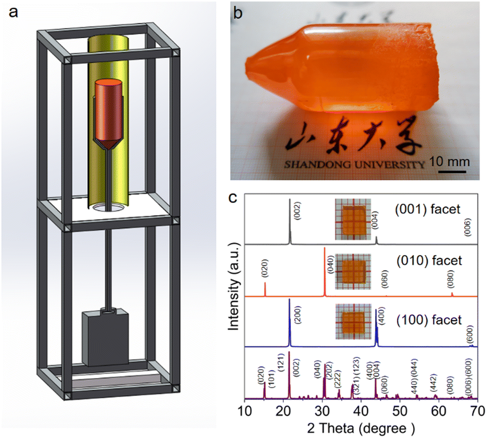 | ||
| Fig. 1 (a) Schematic diagram of the vertical Bridgman furnace. (b) Photograph of an as-grown CsPbBr3 single crystal. (c) XRD patterns of the (100), (010), and (001) wafers. The insets are photographs of the processed and polished wafers. | ||
In addition to purifying the raw materials, cracking must be prevented to obtain large-size CsPbBr3 single crystals. When the temperature gradually decreases from the melting point to room temperature, the phase of CsPbBr3 will change from cubic to tetragonal at 130 °C, and then to orthorhombic at 88 °C. The large thermal expansion coefficient near 130 °C usually results in a severe crack in CsPbBr3 during the cooling process and reduces the quality of the crystal. When the cooling rate was decreased to 10–20 °C h−1, there was less cracking. Fig. 1b shows as-grown CsPbBr3 single crystals with the size of Φ 36 mm × 50 mm. After the bulk CsPbBr3 SC was oriented, the crystal was processed into the (100), (010), and (001) wafers with a thickness of 1.5 mm. The photographs of the wafers in Fig. 1b demonstrate the satisfactory crystallization uniformity of the crystal. The X-ray diffraction (XRD) patterns confirmed the orientations of the wafers (Fig. 1c).
3.2. Structural anisotropy and charge carrier transport properties
The structure of the crystals, including the atomic arrangement, ion densities, and bond strengths, depends on the anisotropic properties. Fig. 2a–c exhibits the arrangement of the [PbBr6]4− octahedrons for the (100), (010), and (001) facets of the CsPbBr3 crystal, respectively. The arrangement of anions and cations at the outmost layers of the three facets is significantly different.23 The Br− ions are terminated at the outmost layers for the (100) and (001) planes, showing negative potentials at the surface of the wafers. For the (010) facet, the Br− anions and Cs+ cations are alternately stopped at the outermost layer, resulting in a charged equilibrium on the surface.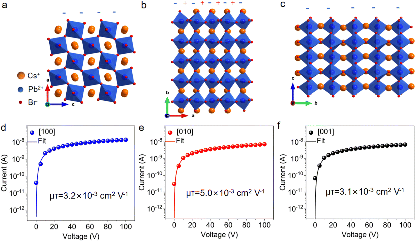 | ||
| Fig. 2 (a–c) Arrangement of [PbBr6]4− octahedrons in the CsPbBr3 crystal structure, and (d–f) photocurrent fitting curves of the [100], [010], and [001] wafers of CsPbBr3 crystal. | ||
The relaxation and reordering of Br− anions and Cs+ cations at the terminal surface can diminish the surface energy, according to the Verwey theory.25 Therefore, the arrangement of anions and cations that are terminated in the outmost layer of the (010) facet reduces the surface energy and inhibits defect recombination at the surface. Moreover, the various stacking arrangements of [PbBr6]4− octahedrons for the (100), (010), and (001) facets lead to differences in charge transport properties along different orientations. As for the [100] and [001] orientations (Fig. 2a), there is an alternate array of the Cs+ ions and [PbBr6]4− octahedrons that forms zigzag chains and reduces the overlap of the Br-p orbital, which suppresses the charge transport. In contrast, continuous connections across [PbBr6]4− octahedrons along the [010] orientation result in strong Br–Pb–Br bonds, which is beneficial for carrier transport.
A large mobility lifetime product (μτ) increases the charge collection efficiency and improves detection performance. Fig. 2d–f compares the mobility lifetime products of the (100), (010), and (001) wafers, whose thicknesses were all 1.5 mm. The mobility lifetime products were obtained by fitting the obtained photocurrent curve with the modified Hecht equation:
 | (1) |
3.3. Anisotropic ion migration properties
It has been recognized that the strong ion migration under large electrical fields in perovskites degrades the performance of devices, leading to the drift of current. Because the migration of ions is strongly related to the structure of the crystal, it is essential to investigate the characteristics of ion migration along different orientations. To quantitatively understand the ionic migration in CsPbBr3 SCs, the activation energies were calculated based on the temperature-dependent current–time curves for applying and removing bias voltages.1A schematic of the typical charging–discharging process is shown in Fig. S2 (ESI†). A bias was applied on the device to promote the movement of ions, and these ions accumulated at the interface between the crystal and electrode. When the ions achieved stability, the bias was abruptly removed, and ions immediately began to travel backward as a result of the high concentration gradient, causing a negative current. As a result, the decay in the negative current curve can be used to evaluate the ion migration, and the activation energy can be fitted using the Arrhenius function from the I–t curves at various temperatures:
 | (2) |
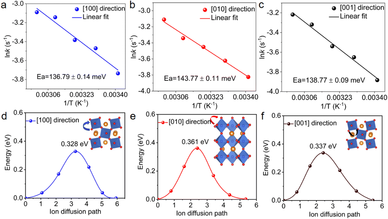 | ||
| Fig. 3 (a–c) Ion migration activation energies of CsPbBr3 crystal wafers along the [100], [010], and [001] directions, respectively. (d–f) Calculated energy profiles of different ionic migration paths for Br− ion vacancy along the [100], [010], and [001] orientations. | ||
First-principles calculations were applied to investigate the anisotropy of ion migration in CsPbBr3. Compared with Pb2+ and Cs+ ions, the Br− ion had the lowest activation energy in CsPbBr3 due to the formation of Br− ion vacancies.26 The insets in Fig. 3d–f present the migration paths for the Br− ion vacancy mechanism along the [100], [010], and [001] orientations. We chose a certain Br ion and calculated energy profiles along [100] (blue), [010] (red), and [001] (black) ionic migration channels. The diffusion barrier of the [010] orientation was calculated as 0.361 eV, which is higher than that of the [100] (0.328 eV) and [001] (0.337 eV) orientations.
This trend is consistent in our experiments, although the experimental results are less than the calculated values due to additional defects in actual crystals, which cause lower activation energy.27 Therefore, the higher activation energy of the (010) wafer and the larger diffusion barrier energy along the [010] orientation demonstrated that there is weaker ion migration for the (010) wafer as compared to the others, which is meaningful for the optimization of the X-ray detection performance in CsPbBr3 devices.
3.4. X-ray detection performance
A high electric field is generally required to enhance the charge collection efficiency and hence increase the sensitivity of the devices. However, the high electric field will result in the migration of ions, which deteriorates the stability of the detector. Fig. 4a schematically illustrates the architecture of the X-ray detector with a simple sandwich structure of EGaIn/CsPbBr3 SC/Au. This asymmetric vertical device constructs a Schottky contact between the EGaIn and CsPbBr3 SC under reverse bias, which decreases the dark current density under a high electrical field.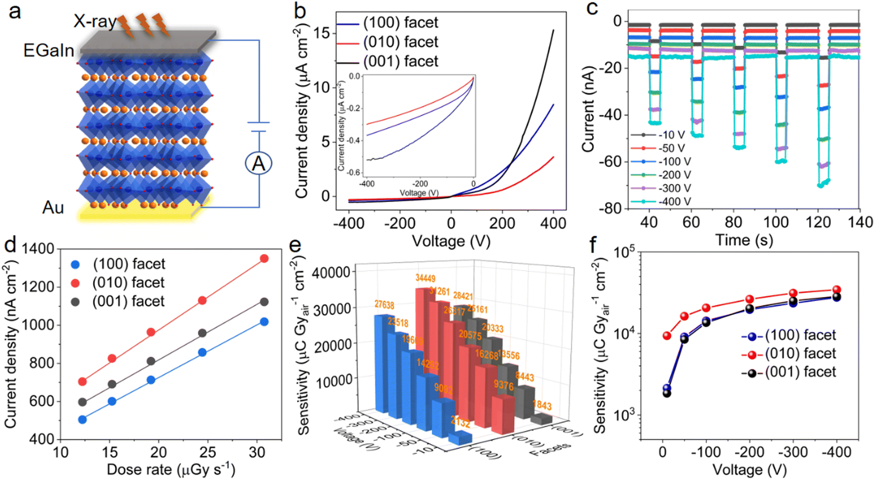 | ||
| Fig. 4 (a) Schematic diagram of the CsPbBr3 detector structure. (b) J–V curves in dark from −400 V to 400 V. The inset shows the enlarged details from −400 V to 0 V. (c) Temporal X-ray responses of the device based on the (010) wafer under voltages from −10 V to −400 V. (d) Photocurrent response via dose rates at −400 V and (e and f) X-ray sensitivities of the (100), (010), and (001) wafers under different voltages. | ||
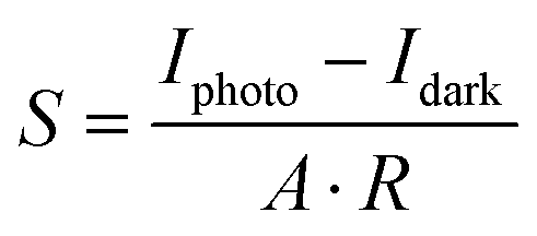
As shown in Fig. 4b, the current density–voltage (J–V) curves of the (100), (010), and (001) wafers based on the same part of the CsPbBr3 SC demonstrated the rectifying characteristics. The (010) wafer presented a lower current density of 0.29 μA cm−2 as compared to those of the (100) wafer (0.36 μA cm−2) and (001) wafer (0.58 μA cm−2) under a bias at −400 V. Fig. 4c and Fig. S6 (ESI†) exhibit time-dependent X-ray responses under 120 keV X-ray photons, with dose rates ranging from 12.23 to 30.73 μGyair s−1 and bias from −10 to −400 V for the (010), (100), and (001) wafers, respectively. When the bias increased to −500 V, the detector demonstrated a severe baseline that was caused by ion migration, as shown in Fig. S7 (ESI†). The sensitivities were calculated using the equation:
 | (3) |
As shown in Fig. 4d and Fig. S8 (ESI†), the X-ray photocurrent densities of the devices were linearly fitted to the dose rates under various bias voltages, and the sensitivities were calculated as 27638, 34449, and 28421 μC Gyair−1 cm−2 under the voltage of −400 V for the (100), (010), and (001) detectors, respectively. Fig. 4e compares the whole sensitivities under different voltages for 120 keV X-ray photons. The sensitivities of the (010) wafer were higher than those of the (100) and (001) wafers.
As the bias increased from −10 to −400 V, the sensitivities of the EGaIn/CsPbBr3 SC/Au detectors gradually increased until saturation (Fig. 4f). The high electric field promotes the diffusion of charge carriers and improves the collection of charges. Once the voltage reaches a certain value, the photoinduced charges are completely collected so that there is saturation of the photocurrent.28 The optimum value of 34449 μC Gyair−1 cm−2 for the (010) detector under the highest bias at −400 V (corresponding to the electric field of −2666 V cm−1) is due to the large μτ product and weak ion migration among the (100), (010), and (001) facets of a single crystal of CsPbBr3. In addition, the sensitivity of the (010) facet detector is three orders of magnitude higher than that of commercial semiconductor α-Se (20 μC Gyair−1 cm−2)2, and five times higher than that of the CZT detector (6069 μC Gyair−1 cm−2).29
Compared with perovskite materials, the sensitivity value is one order of magnitude higher than that of the MAPbI3 detector (1471.7 μC Gyair−1 cm−2)30 and CsPbI3 detector (2370 μC Gyair−1 cm−2),31 and two orders of magnitude higher than that of the FAPbI3 detector (130 μC Gyair−1 cm−2)32 and MAPbBr3 detector (6169 μC Gyair−1 cm−2).33
The current drift D was applied to investigate the stability of the detectors, which is calculated as:
| D = (Jt − J0)/(t·E) | (4) |
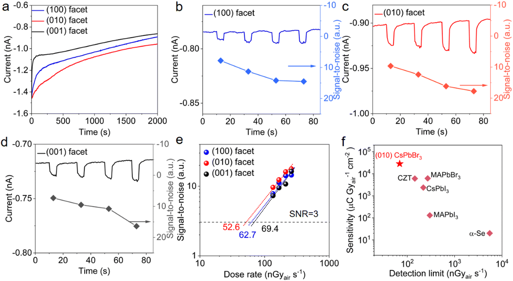 | ||
| Fig. 5 (a) Comparison of dark current drifts for the (100), (010), and (001) CsPbBr3 crystal detectors under a bias voltage of −10 V. (b–d) Responses and SNR values dependent on X-ray dose rates from 135 to 260 nGyair s−1 for the (100), (010), and (001) CsPbBr3 crystal devices when a 2 mm-thick Pb shielding case was inserted between the detector and the X-ray source. (e) Detection limits that are derived from the fitting line with an SNR of 3. (f) Comparison of X-ray detection performance of semiconductor detectors. | ||
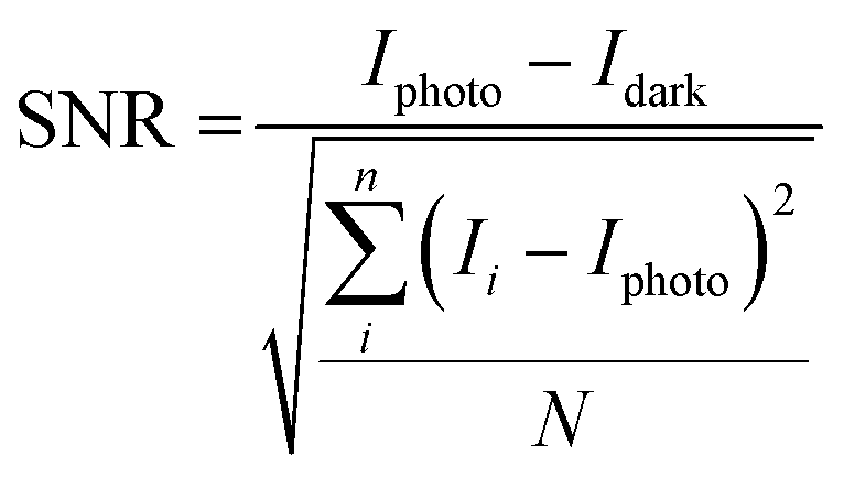
The detection limit, which was defined as the dose rate with a signal-to-noise (SNR) value of 3, is another important parameter to use for evaluating the performance of the X-ray device. The SNR ratio of the device under various dose rates can be calculated, as follows:
 | (5) |
Fig. 5e compares the detection limits of three wafers, which were derived from the fitting line with an SNR of 3. The (010) device exhibited the lowest detection limit of 52.6 nGyair s−1, which was approximately two orders of magnitude lower than the standard medical diagnostic requirement of 5.5 μGyair s−1.1 Moreover, the detection limit of our CsPbBr3 SC is two times lower than that of the CZT detector (145 nGyair s−1),29 and four times lower than that of the CsPbI3 detector (219 nGyair s−1),31 MAPbBr3 detector (271 nGyair s−1),33 and FAPbBr3 detector (300 nGyair s−1).32
Fig. 5f and Table 1 compare the X-ray detection performance of reported commercial semiconductors and perovskites. It reveals that our (010) facet of the CsPbBr3 SC device displays the highest sensitivity and the lowest detection limit compared to other reported SC devices. Moreover, our CsPbBr3 SC device exhibited long-term stability under ambient conditions for 10 days with negligible change even when the air humidity reached 60% (Fig. S9, ESI†). In summary, the (010) wafer in CsPbBr3 SC demonstrated optimal X-ray detection properties including high sensitivity, low detection limit, large ion activation energy, and small current drift, providing an approach to optimize X-ray detection devices by controlling the orientations of crystals.
| Device structure | X-ray source (keV) | Electric field (V cm−1) | Sensitivity (μC Gyair−1 cm−2) | Detection limit (nGyair s−1) | Ref. |
|---|---|---|---|---|---|
| α-Se | 20 | — | 20 | 5500 | 2 |
| Au/CZT SC/Au | 120 | 5000 | 6069 | 145 | 29 |
| Au/MAPbI3 SC/Au | 100 | 33 | 1471.7 | 46000 |
30 |
| Au/CsPbI3 SC/Au | 50 | 41.7 | 2370 | 219 | 31 |
| Au/MAPbBr3 SC/Au | 120 | 150 | 6169 | 271 | 33 |
| Au/FAPbBr3 SC/Au | 50 | 50 | 130 | 300 | 32 |
| EGaIn/(100) CsPbBr3 SC/Au | 120 | 2666 | 27638 |
62.7 | This work |
| EGaIn/(010) CsPbBr3 SC/Au | 120 | 2666 | 34449 |
52.6 | This work |
| EGaIn/(001) CsPbBr3 SC/Au | 120 | 2666 | 28421 |
69.4 | This work |
4. Conclusions
We grew CsPbBr3 SCs with the size of Φ 36 mm × 50 mm using a modified Bridgman method. The [100], [010], and [001] orientations of the bulk crystal were determined for X-ray detector fabrication. The structural anisotropy resulted in distinctions in defect densities and charge carrier transport properties. The detector with the [010] orientation of CsPbBr3 SC exhibited a large activation energy (143.77 meV) and ion diffusion barrier energy (0.361 eV), which indicated weak ion migration. The (010) device achieved optimal sensitivity of 34449 μC Gyair−1 cm−2 and a detection limit of 52.6 nGyair s−1 for 120 keV X-ray detection. Our findings imply that the selection of the crystal direction is an efficient method for optimizing X-ray radiation detection in perovskite crystals.
Conflicts of interest
There are no conflicts to declare.Acknowledgements
This work was financially supported by the National Natural Science Foundation of China (Grant No. 62274103, 51972194, and 51932004), the National Key R&D Program of China (Grant No. 2022YFB3204101 and 2018YFB0406502), and the 111 Project 2.0 (Grant No. BP2018013).Notes and references
- W. Pan, H. Wu, J. Luo, Z. Deng, C. Ge, C. Chen, X. Jiang, W. Yin, G. Niu, L. Zhu, L. Yin, Y. Zhou, Q. Xie, X. Ke, M. Sui and J. Tang, Nat. Photonics, 2017, 11, 726 CrossRef CAS.
- H. Wu, Y. Ge, G. Niu and J. Tang, Matter, 2021, 4, 144–163 CrossRef CAS.
- Y. He, M. G. Kanatzidis and I. Hadar, Nat. Photonics, 2021, 16, 14 CrossRef.
- G. J. Matt, I. Levchuk, J. Knüttel, J. Dallmann, A. Osvet, M. Sytnyk, X. Tang, J. Elia, R. Hock, W. Heiss and C. J. Brabec, Adv. Mater. Interfaces, 2020, 7, 1901575 CrossRef CAS.
- Y. Hua, F. Cui, P. Zhang, G. Zhang, Q. Zhang and X. Tao, Z. Anorg. Allg. Chem., 2022, 648, e202200025 CrossRef CAS.
- X. Li, P. Zhang, Y. Hua, F. Cui, X. Sun, L. Liu, Y. Bi, Z. Yue, G. Zhang and X. Tao, ACS Appl. Mater. Interfaces, 2022, 14, 9340 CrossRef CAS.
- S. Dong, Z. Hu, P. Wei, J. Han, Z. Wang, J. Liu, B. Su, D. Zhao and Y. Liu, Adv. Mater., 2022, 34, e2204342 CrossRef.
- G. Nazir, S. Lee, J. Lee, A. Rehman, J. Lee, S. Seok and S. Park, Adv. Mater., 2022, 34, e2204380 CrossRef PubMed.
- S. Chu, Y. Zhang, P. Xiao, W. Chen, R. Tang, Y. Shao, T. Chen, X. Zhang, F. Liu and G. Zheng, Adv. Mater., 2022, 34, e2108939 CrossRef.
- Y. Zhou, M. Parkes, J. Zhang, Y. Wang, M. Ruddlesden, H. Fielding and L. Su, Sci. Adv., 2022, 8, eabq8629 CrossRef CAS.
- Y. He, M. Petryk, Z. Liu, D. G. Chica, I. Hadar, C. Leak, W. Ke, I. Spanopoulos, W. Lin, D. Chung, B. W. Wessels, Z. He and M. G. Kanatzidis, Nat. Photonics, 2021, 15, 36 CrossRef CAS.
- Q. Fan, H. Xu, S. You, Y. Ma, Y. Liu, W. Guo, X. Hu, B. Wang, C. Gao, W. Liu, J. Luo and Z. Sun, Small, 2023, 2301594 CrossRef.
- C. Li, F. Chen, K. Wang, Q. Yao, J. Zhang, Q. Zhao, Q. Huang, H. Zhu and J. Ding, J. Mater. Chem. C, 2022, 10, 14580 RSC.
- W. Guo, X. Liu, S. Han, Y. Liu, Z. Xu, M. Hong, J. Luo and Z. Sun, Angew. Chem., Int. Ed., 2020, 59, 13879 CrossRef CAS PubMed.
- P. Zhang, G. Zhang, L. Liu, D. Ju, L. Zhang, K. Cheng and X. Tao, J. Phys. Chem. Lett., 2018, 9, 5040 CrossRef CAS PubMed.
- F. Chen, C. Li, C. Shang, K. Wang, Q. Huang, Q. Zhao, H. Zhu and J. Ding, Small, 2022, 18, 2203565 CrossRef CAS.
- R. Toufanian, S. Swain, P. Becla, A. Datta and S. Motakef, J. Mater. Chem. C, 2022, 10, 12708 RSC.
- Y. He, I. Hadar, M. C. De Siena, V. V. Klepov, L. Pan, D. Chung and M. G. Kanatzidis, Adv. Funct. Mater., 2022, 32, 2112925 CrossRef CAS.
- L. Pan, Y. He, V. V. Klepov, M. C. De Siena and M. G. Kanatzidis, IEEE Trans. Med. Imaging, 2022, 41, 3053 Search PubMed.
- N. K. Tailor and S. Satapathi, J. Phys. Chem. C, 2022, 126, 17789 CrossRef CAS.
- M. H. Huang, G. Naresh and H. Chen, ACS Appl. Mater. Interfaces, 2018, 10, 4 CrossRef CAS.
- C. Tan, S. Hsu, W. Ke, L. Chen and M. H. Huang, Nano Lett., 2015, 15, 2155 CrossRef CAS PubMed.
- J. Ding, L. Jing, Y. Yuan, J. Zhang, Q. Yao, K. Wang, W. Zhang, H. Sun, B. Liu, T. Zhou and X. Zhan, ACS Appl. Energy Mater., 2020, 3, 10525 CrossRef CAS.
- L. Zhang, S. Cui, Q. Guo, C. Ge, Q. Han, Q. Lin, C. Li, X. Zheng, Z. Zhai, L. Wang, Q. Sun, Y. Xu, Y. Liu and X. Tao, ACS Appl. Mater. Interfaces, 2020, 12, 51616 CrossRef CAS.
- H. Ohshima, Electrical Phenomena at Interfaces and Biointerfaces: Fundamentals and Applications in Nano-, Bio-, and Environmental Sciences, John Wiley & Sons, Inc., 2012, p. 27 Search PubMed.
- B. Zhang, F. Wang, H. Zhang, B. Xiao, Q. Sun, J. Guo, A. B. Hafsia, A. Shao, Y. Xu and J. Zhou, Appl. Phys. Lett., 2020, 116, 063505 CrossRef CAS.
- B. Yang, W. Pan, H. Wu, G. Niu, J. Yuan, K. Xue, L. Yin, X. Du, X. Miao, X. Yang, Q. Xie and J. Tang, Nat. Commun., 2019, 10, 1989 CrossRef PubMed.
- X. Wang, D. Zhao, Y. Qiu, Y. Huang, Y. Wu, G. Li, Q. Huang, Q. Khan, A. Nathan, W. Lei and J. Chen, Phys. Status Solidi RRL, 2018, 12, 1800380 CrossRef.
- P. Zhang, Y. Hua, Y. Xu, Q. Sun, X. Li, F. Cui, L. Liu, Y. Bi, G. Zhang and X. Tao, Adv. Mater., 2022, 34, e2106562 CrossRef PubMed.
- X. Geng, H. Zhang, J. Ren, P. He, P. Zhang, Q. Feng, K. Pan, G. Dun, F. Wang, X. Zheng, H. Tian, D. Xie, Y. Yang and T. Ren, Appl. Phys. Lett., 2021, 118, 063506 CrossRef CAS.
- B. Zhang, X. Liu, B. Xiao, A. B. Hafsia, K. Gao, Y. Xu, J. Zhou and Y. Chen, J. Phys. Chem. Lett., 2020, 11, 432 CrossRef CAS.
- M. Yao, J. Jiang, D. Xin, Y. Ma, W. Wei, X. Zheng and L. Shen, Nano Lett., 2021, 21, 3947 CrossRef CAS.
- W. Li, H. Li, J. Song, C. Guo, H. Zhang, H. Wei and B. Yang, Sci. Bull., 2021, 66, 2199 CrossRef CAS.
- M. Xia, J. Yuan, G. Niu, X. Du, L. Yin, W. Pan, J. Luo, Z. Li, H. Zhao, K. Xue, X. Miao and J. Tang, Adv. Funct. Mater., 2020, 30, 1910648 CrossRef CAS.
Footnotes |
| † Electronic supplementary information (ESI) available. See DOI: https://doi.org/10.1039/d3tc01085f |
| ‡ These authors contributed equally to this work. |
| This journal is © The Royal Society of Chemistry 2023 |