
Enhancing chemisorption efficiency and thin-film characteristics via a discrete feeding method in high-k dielectric atomic layer deposition for preventing interfacial layer formation†
Ae Jin
Lee
,
Seungwoo
Lee
 ,
Dong Hee
Han
,
Youngjin
Kim
and
Woojin
Jeon
*
,
Dong Hee
Han
,
Youngjin
Kim
and
Woojin
Jeon
*
Department of Advanced Materials Engineering for Information and Electronics, and Integrated Education Program for Frontier Science & Technology (BK21 Four), Kyung Hee University, Yongin, Gyeonggi 17104, Korea. E-mail: woojin.jeon@khu.ac.kr
First published on 2nd May 2023
Abstract
Interfacial layer formation between electrodes and insulators is a well-known issue in metal–insulator–metal capacitors and can severely limit their electrical properties. In this study, we investigate the use of the discrete feeding method (DFM) in atomic layer deposition (ALD) to prevent the degradation of electrical properties caused by the interfacial layer. Our results show that the DFM can significantly improve the chemisorption efficiency of precursors, increase the growth rate, and reduce deposition time in ALD. Furthermore, we demonstrate that the thin-film characteristics can be improved through dense chemisorption of precursors. By applying the DFM to the deposition of ZrO2, which is commonly used as an insulator in dynamic random-access memory capacitors, we show that interfacial layer formation can be prevented. We confirm the effectiveness of the DFM by comparing the effects of different precursor sizes, analyzing the chemical states of Zr and Ti, and performing AC non-linearity and equivalent oxide thickness analyses. These findings provide new insights into the origin and solution of interfacial layer formation in metal–insulator–metal capacitors and have important implications for the development of electronic devices.
 Woojin Jeon | Professor Woojin Jeon received his Bachelor's and Master's degrees from the Department of Materials Science and Engineering of the Korea Advanced Institute of Science and Technology (KAIST) in 2005 and 2007, respectively, and his PhD degree from the same department of Seoul National University (Korea) in 2015. His current research interests focus on semiconductor materials, devices, and processing, drawing from his extensive research experience in domestic and foreign research institutes such as KIST and CNRS/CEA-LETI, as well as in industries such as SK Hynix Inc. and Samsung Advanced Institute of Technology. Currently, he serves as an associate professor in the Department of Advanced Materials Engineering for Information and Electronics at Kyung Hee University in Korea. |
Introduction
High dielectric constant (k) materials, such as ZrO2, TiO2, and SrTiO3, have been investigated as insulating layers to enhance the performance of dynamic random access memory (DRAM) capacitors. Among them, TiO2 and SrTiO3 have attracted considerable attention because of their high k values (k = 90–250). However, employing new high-k materials in actual devices is limited because of the need to apply a noble metal electrode or the leakage current problem in thin-films with a physical thickness of below 5 nm. Therefore, despite a relatively low k value of less than 40,1 ZrO2-based thin films with TiN electrodes have been adopted for metal–insulator–metal (MIM) capacitors for DRAM applications for over a decade. Further improvement of the TiN/ZrO2-based structure is necessary for its application in next-generation DRAM devices. However, decreasing the thickness of each component in a DRAM capacitor to below 5 nm is difficult in the deposition process and leads to leakage current degradation, such as inducing a tunneling current. Additionally, at the interface of different thin films, the interface of the electrode and insulator in the MIM capacitor case, an interfacial layer is formed owing to numerous reasons, such as differences in the crystal structure. However, although the thickness of the dielectric film is reduced, the interfacial layer does not decrease proportionally. Hence, decreasing the physical thickness of the insulator increases the proportion of the interfacial layer and may occupy more than 10% of the total dielectric film. The formation of an interfacial layer results in capacitance reduction because such a layer has a low relative permittivity.1–3 Additionally, interfacial layers induce leakage current degradation by acting as trap sites. The reliability of a DRAM capacitor is also deteriorated by its interfacial characteristics.4–7 Eventually, interfacial characteristics degrade the electrical properties of an entire MIM capacitor.The mechanism of interfacial layer formation has not yet been clearly elucidated. In particular, for the TiN and ZrO2 interfaces, two mechanisms were suggested for interfacial layer formation. First, owing to the difference in chemical reactivity with oxygen between TiN and ZrO2, the oxygen scavenging effect of the deposited ZrO2 thin film occurred on the TiN substrate; the oxygen of ZrO2 moved to TiN, thereby resulting in the formation of a TiON layer at the surface of the TiN substrate as well as the formation of oxygen vacancies in ZrO2, which is denoted ZrO2−x (x < 1).6,8 During the early stage of the atomic layer deposition (ALD) process of ZrO2, the unoccupied precursor chemisorption site on the TiN surface is exposed to the oxidant of the ZrO2 ALD process, thus resulting in the formation of an interfacial layer of TiON at the TiN surface.5 The redox reaction between TiN and ZrO2 is difficult to suppress because it originates from the oxidation potential difference, which is an inherent property. However, oxidation of the TiN surface by the oxidant in the ZrO2 ALD process can be avoided.
The steric hindrance effect, a factor that interferes with the adsorption behavior of a precursor, is a phenomenon wherein precursors cannot reach the chemisorption sites because of the physical size of the ligand of the adjacent precursors.9–11 In the ideal case, when the chemisorption sites are fully occupied, the exposed area of the TiN surface is an inherent property because the steric hindrance effect only governs the exposed area. In this regard, the area exposed by the steric hindrance effect depends on the precursor employed in the ALD process; in turn, this is inherent. However, in the actual ALD process, an excess precursor is introduced into the chamber, and the chemisorption and physisorption of the precursor occur simultaneously. During this stage, some part of the physisorbed precursor screens the unoccupied chemisorption site, unintentionally, thereby reducing the precursor chemisorption density, which is called the “screening effect”.11–14 Accordingly, the screening effect is one of the mechanisms that increases the exposed area in the early stage of the insulator ALD process. In contrast to the steric hindrance effect, the screening effect can be effectively eliminated by reducing the physisorbed precursor. To reduce the physisorbed precursor, the discrete feeding method (DFM) was employed herein.
DFM was developed to increase the growth rate of ALD. The DFM is a method that splits the precursor feeding–purging step of the conventional ALD several times.9,11–13 This facilitates the effective chemisorption of precursors by adding a “cut-in purge” to the total precursor feeding time. The cut-in purge of the DFM removes the physisorbed precursors in the precursor feeding step and exposes the screened and unoccupied chemisorption sites to the subsequently introduced precursor. Thus, the precursors can be densely adsorbed into the chemisorption sites during the subsequent precursor feeding step. More adsorption is achieved with the same feeding time, thus inducing an increase in the growth rate.9,12,14 Therefore, employing the DFM in the insulator ALD process can effectively reduce the exposed area of the TiN surface to the oxidant of the ALD process.
Experimental details
ZrO2 thin films were deposited using ALD (iOV dX1, iSAC Research) with cyclopentadienyltris(dimethylamino)zirconium (CpZr[N(CH3)2]3, CpZr, SKtrichem) and tetrakis-ethylmethylamino-zirconium (Zr [N(CH3)(C2H5)]4, TEMAZ, SKtrichem). O3 was used as an oxygen source at a concentration of 170 g m−3. The canisters of CpZr and TEMAZ were maintained at 80 and 60 °C, respectively, to acquire the appropriate vapor pressures of each precursor. The deposition temperatures were set to 300 and 270 °C to deposit ZrO2 thin films using CpZr and TEMAZ, respectively. The conventional ALD sequences for the base of ZrO2 film deposition using CpZr and TEMAZ as the Zr precursor contained Zr precursor feeding, Ar purge, O3 feeding, and Ar purging steps of 7–10–3–20 s and 3–10–3–10 s, respectively. The sequence of employing the DFM on the ALD was performed by dividing the precursor feeding–purging steps into five times [(1.4–2) × 5]–3–10 s for CpZr and three times [(1–3.3) × 3]–3–10 s for TEMAZ (Fig. 1). The substrate contained 50 nm-thick TiN as the bottom electrode on a thermally oxidized (100) Si wafer. Postdeposition annealing was performed at 600 °C for 30 s under a N2 atmosphere using a rapid thermal process. To measure the electrical properties, an MIM capacitor was fabricated with a top electrode containing 10 nm-thick TiN and 50 nm-thick Pt film deposited via DC sputtering, defined by a metal shadow mask with a 300 μm diameter hole.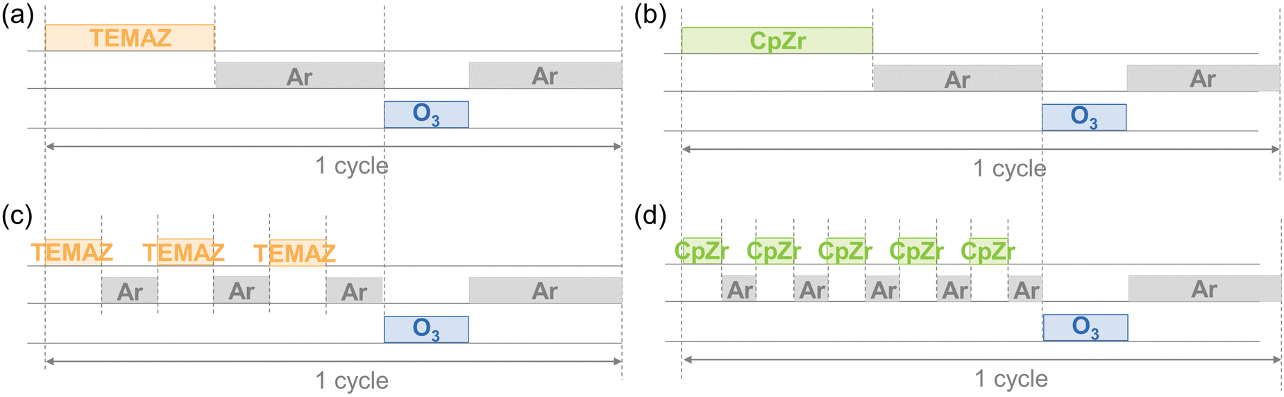 | ||
| Fig. 1 Schematic of the ALD process sequences of base sequence with (a) TEMAZ (TEMAZbase), (b) CpZr (CpZrbase), and DFM sequence with (c) TEMAZ (TEMAZDFM), (d) CpZr (CpZrDFM). | ||
The film thickness was determined by calculating the layer density, which was measured using X-ray fluorescence spectroscopy (ARL Quant’X, Thermo ScientificTM) and was correlated with spectroscopic ellipsometry (ESM-300, J. A. Woollam) measurements and transmission electron microscopy (TEM, JEM-2100F) images. Glancing angle incident X-ray diffraction (GA-XRD, X’pert Pro, PANalytical) with an incident angle of 0.5° was used to examine the crystal structures of the films. The densities of the ZrO2 films were measured using X-ray reflectivity (XRR, X’pert Pro, PANalytical). The electrical properties were evaluated by measuring the capacitance versus voltage and capacitance versus frequency using Agilent 4284, and the current versus voltage characteristics were measured using an Agilent 4155C semiconductor parameter analyzer.
Results and discussion
The change in the growth rate (growth per cycle, GPC) was investigated by employing DFM depending on the precursors. As shown in Fig. 2(a), the GPC of the ZrO2 thin film with TEMAZ as a base sequence (TEMAZbase) of 0.129 nm per cycle was relatively higher than that of CpZr with a base sequence (CpZrbase) of 0.105 nm per cycle. This difference originates from the steric hindrance effect difference; the relatively bulky cyclopentadienyl ligand induces a greater steric hindrance effect.15 The GPC values when employing the DFM cases for both precursors increased to 0.150 and 0.110 nm per cycle for TEMAZ (TEMAZDFM) and CpZr (CpZrDFM), respectively. To investigate the GPC change in more detail, the differentiating growth rate (ΔGPC) of the ZrO2 thin film as a function of the number of ZrO2 ALD cycles is depicted in Fig. 2(b), acquired from the data in Fig. 2(a). Evidently, the trends in ΔGPC for all the cases exhibited identical behavior. In all cases, up to 30 cycles of ALD, ΔGPC values decreased with the increasing number of ALD cycles. This result indicates that both precursors had a higher chemisorption density on the TiN substrate than on the ZrO2 thin film. Furthermore, the increment in the ΔGPC by employing the DFM compared with the base condition for each ALD process using TEMAZ and CpZr, i.e. TEMAZDFM – TEMAZbase and CpZrDFM – CpZrbase, respectively, was investigated (Fig. 2(c)). Given that the growth rate in the ALD process was determined by the amount of chemisorbed precursor, the increment value directly indicates the increasing amount of the chemisorbed precursor by employing the DFM, that is, the screening effect on the growth rate. In contrast to Fig. 2(b), the increment varied with the cycle number and exhibited different behaviors depending on the employed precursor. In the case of TEMAZ, the increment was constant at 0.022 nm per cycle, regardless of the cycle number. However, the increment in the case of CpZr was 0.013 nm per cycle at the beginning and gradually decreased to 0.0084 nm per cycle at 100 cycles. Moreover, in the overall cycle number, the increment in the case of CpZr was much smaller than that in the TEMAZ case. The comparison between the TEMAZ and CpZr cases revealed that the screening effect of the physisorbed precursor was influenced by the physical size of the ligand in the precursor; the precursor with the smaller ligand exhibited a higher screening effect. Essentially, the screening effect is dominant when the chemisorption density of the precursor is high. In the case of CpZr, a significant increment in ΔGPC was observed at 10 cycles, where the chemisorption density of CpZr was the highest.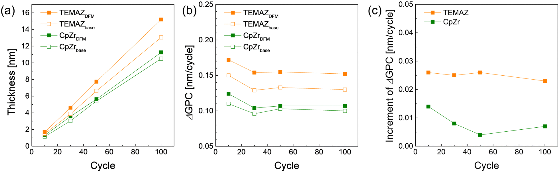 | ||
| Fig. 2 (a) ZrO2 thin film thickness, (b) differential growth rate (ΔGPC), and (c) increment of growth rate with respect to the cycle number varied by employing precursors and sequence. | ||
The physical and chemical status of the deposited ZrO2 thin film, and the formation of the interfacial layer influenced by the screening effect during ZrO2 thin film deposition were investigated (Table 1 and Fig. 3). Evidently, the film density deposited by ALD was strongly influenced by the chemisorption density of the precursor.15,16 In the case deposition by the base sequence, the ZrO2 thin film using TEMAZbase exhibited a relatively higher film density of 5.20 g cm−3 compared with that of CpZrbase (5.00 g cm−3). This is because TEMAZ has a relatively higher chemisorption density compared with that of CpZr because of the steric hindrance effect. In this regard, the film density in the case employing DFM was increased to 5.50 and 5.11 g cm−3 for TEMAZDFM and CpZrDFM, respectively. Moreover, the TEMAZDFM case exhibited a greater increase compared with that of CpZrDFM, which was consistent with the increase in ΔGPC. The oxygen vacancy (VO) concentration of the 3 nm ZrO2 thin film deposited on TiN was quantified from the Zr 3d XPS spectra (Fig. 3(a)–(d)). Owing to the high chemical reactivity of the bottom TiN layer, Ti in TiN acquires oxygen from ZrO2 during oxidation, thereby forming oxygen-deficient ZrO2−x (x < 1). In the Zr 3d5/2 peaks, binding energies of 182.3 and 181.8 eV correspond to the energy of ZrO2 and ZrO2−x, respectively.17 The ZrO2−x peak with a lower binding energy indicates a less oxidized Zr ion; therefore, ZrO2−x represents interfacial layer formation by the oxygen scavenging effect caused by the chemical reactivity difference with oxygen between TiN and ZrO2.5 In the case of ZrO2, the ratio values of ZrO2−x to ZrO2 for all cases were almost identical at below 0.1, which is lower than the error margin from deconvolution. Therefore, this implies that the formation of ZrO2−x was intrinsically independent of the employed precursor and deposition procedure. Simultaneously, TiN may be oxidized to form TiON, which is one of the suggested mechanisms for the formation of the interfacial layer.4,18,19 In the Ti 2p spectra, the 2p3/2 peak was deconvoluted into peaks at the binding energy of 454.6 and 458.4 eV corresponding to Ti–N and Ti–O–N bonding, respectively.18 Due to air exposure, the TiN substrate has an oxidized surface of TiON, inevitably. While performing the ZrO2 ALD process, the TiN substrate was further oxidized and TiON formation occurred (Fig. S1 in ESI†). In contrast to the Zr 3d case, the formation of TiON was strongly affected by the Zr precursor. Under the base conditions, the ratio of TiON to TiN (TiON/TiN) was much higher in TEMAZbase (3.03) than in CpZrbase (1.94). However, in the case of employing DFM, the difference in TiON/TiN between CpZrDFM and TEMAZDFM was reversed: twice as high in CpZrDFM (1.75) than in TEMAZDFM (0.808). This was because CpZr exhibited a slight (1.94 to 1.75) and a dramatic decrease in TEMAZ (3.03 to 0.808). The result implies that in contrast to the ZrO2−x formation, the interfacial layer formation of TiON on TiN was strongly influenced by the exposed area of the TiN surface.
| TEMAZ | CpZr | |||
|---|---|---|---|---|
| Base | DFM | Base | DFM | |
| ZrO2−x/ZrO2 | 0.062 | 0.038 | 0.060 | 0.034 |
| TiON/TiN | 3.03 | 0.808 | 1.94 | 1.75 |
| Density of ZrO2 [g cm−3] | 5.20 | 5.50 | 5.00 | 5.11 |
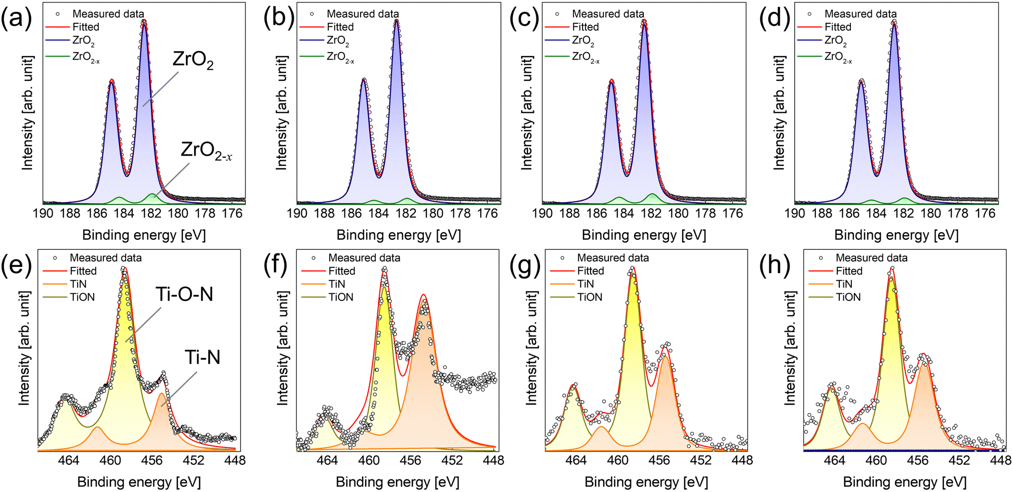 | ||
| Fig. 3 XPS spectra of (a)–(d) Zr 3d and (e)–(h) Ti 2p of ZrO2 thin film deposited on TiN substrate using (a), (e) TEMAZbase, (b) and (f) TEMAZDFM, (c) and (g) CpZrbase, and (d) and (h) CpZrDFM. | ||
From the above results, the interfacial layer formation mechanism of TiON on TiN/ZrO2 can be described by a schematic of the chemisorption behavior of the Zr precursor on TiN with respect to the employed precursor and sequence (Fig. 4). In the case of TEMAZbase (Fig. 4(a) and (b) depict precursor feeding and precursor purge steps, respectively), exposure of the TiN surface on the oxidant of the ZrO2 ALD sequence during the O3 feeding step was inevitable because of the relatively small physical size of the ligand. Moreover, the screening effect affected the chemisorption density of TEMAZ in the base sequence, thereby resulting in an increase in the number of unoccupied chemisorption sites, even after the precursor purge step (Fig. 4(b)). Consequently, TiON formation at the surface of TiN should be severe because of the considerable exposure area of the TiN surface to O3. In the case of CpZrbase, an unoccupied chemisorption site was formed (Fig. 4(e) and (f)) by the screening effect, as in the case of TEMAZbase. However, in the CpZr case, the unoccupied sites were also considerably screened by the steric hindrance effect originating from the large physical dimension of the Cp ligand to the extent that chemisorption was significantly limited. In this regard, as the reach of the precursor on the surface was hindered, substrate exposure by O3 in the subsequent ZrO2 ALD process was limited by the steric hindrance effect. Consequently, although the chemisorption density of CpZr was lower than that of TEMAZ in terms of GPC and film density, TiON formation was lower in CpZrbase than in TEMAZbase. This difference in the precursor strongly affected the change in the TiON interfacial layer formation when employing DFM. As depicted in Fig. 2(c), the increase in GPC of CpZrDFM was almost negligible. This indicates that the steric hindrance effect was too decisive in the case of using a precursor with a physically large ligand, such as CpZr, thus causing no additional chemisorption, whereas the screening effect was removed by eliminating the physisorbed precursor using DFM (Fig. 4(h)). Moreover, this implies that the O3 exposure area of the surface under the CpZrbase condition was diminutive. In this regard, the difference in the exposure area between CpZrDFM and CpZrbase was small; hence, the ratio of TiON/TiN slightly decreased even when employing the DFM. Following the elimination of the ligand, which induced the steric hindrance effect by the O3 feeding step, the formation of TiON by the TiN surface exposed to excess O3 was intrinsically unavoidable. Therefore, the TiON interfacial layer formation was suppressed only limitedly when CpZr was used. The electrostatic repulsive effect of Cp ligand can also contribute to the behavior in the DFM. Since the Cp ligand has highly localized charge density,22 the precursor containing Cp ligands exerts a large electrostatic repulsive force on each other. This repulsive force could suppress the chemisorption as well as physisorption, which induces the screening effect. In this regard, the CpZr cases did not exhibited any significant difference between the base and the DFM. And, the TiON formation was relatively higher in CpZr cases than in the TEMAZ cases. However, in the case of TEMAZ, the screening effect predominantly affected the film deposition behavior because the steric hindrance effect was negligible. This indicates that when TEMAZ was introduced on the surface after conducting the cut-in purge (Fig. 4(b) and (c)), the unoccupied chemisorption site, screened by the physisorbed precursor (Fig. 4(a)), was densely occupied by introduced precursors during second feeding (Fig. 4(c) and (d)). The significant increase in the GPC and film density in the TEMAZDFM case also indicates an increase in the chemisorption precursor density when the DFM was applied. Consequently, the exposure area of the TiN surface to O3 was substantially decreased, thus resulting in the effective suppression of TiON interfacial layer formation.
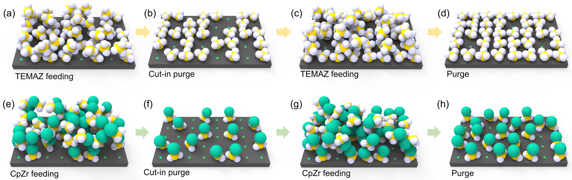 | ||
| Fig. 4 Schematic diagram for depicting the precursor feeding procedure of TEMAZbase (a and b), TEMAZDFM (a–d), CpZrbase (e–f)) and CpZrDFM (e–h) in the ZrO2 ALD process. | ||
Fig. 5 shows the AC non-linear character of the MIM structures of the 10 nm-thick-ZrO2 thin films deposited with various precursors and sequences. The AC nonlinearity measurement was performed by modulating the AC level during capacitance–voltage measurement with a fixed DC bias and frequency.20 This induces charging and discharging of the defect corresponding to the applied AC level. Consequently, the relatively increased capacitance (C/C0, where C0 denotes the capacitance density of the AC level of 0 V) with respect to the increased AC level qualitatively indicates the defect density. Moreover, the defect density difference based on the location in the dielectric thin film was evaluated by applying a DC bias. In this work, as the signal was applied to the top electrode and the bottom electrode was grounded, the conditions of applying a DC bias of –0.5, 0, and +0.5 V represent the interface of top TiN and ZrO2, bulk region of ZrO2, and interface of bottom TiN and ZrO2, respectively. As shown in Fig. 5, the AC nonlinearity changed depending on the applied DC bias. At a DC bias of −0.5 V, where the interface of the top electrode and ZrO2 contributed, C/C0 did not change in either TEMAZ or CpZr. This is because the interface between the top electrode and ZrO2 was not influenced by the deposition conditions of the insulator. In contrast, C/C0 values were changed by applying the DFM at DC biases of 0 and +0.5 V in both CpZr and TEMAZ precursor cases. Moreover, the decreasing C/C0 in the case of the DFM was gradually increased by increasing the DC bias from 0 to +0.5 V. First, the change in the C/C0 depending on the DC bias exhibited a gradual increase with a DC bias of −0.5, 0, and +0.5 V for both CpZr and TEMAZ cases, thus indicating that the defect density contributing to the trap and detrap was increased in the insulator, along with the thickness direction from the interface with the top electrode to the interface with the bottom electrode. This implies that the defect generation at the interface of the bottom electrode and insulator was significantly more severe than that in the other regions of the insulator. The relatively harsh defect generation at the bottom electrode was reduced when employing DFM. Both MIM capacitors deposited with the CpZrDFM and TEMAZDFM sequences exhibited a decreased C/C0 at a DC bias of +0.5 V compared with CpZrbase and TEMAZbase. Simultaneously, C/C0 at a DC bias of 0 V also decreased. This suggests that the defect density in the bulk region of the ZrO2 thin film is also influenced by the properties of the interface with the bottom electrode. Furthermore, C/C0 values in all cases of CpZr were higher than those of TEMAZ. As the TEMAZbase case exhibited an almost identical ZrO2−x ratio and a relatively higher TiON ratio compared with the CpZr cases (Table 1), other factors were also assumed to govern the C/C0 characteristics along with the interface properties depicted in the formation of ZrO2−x and TiON. Meanwhile, applying the DFM reduced the C/C0 values at the 0 and +0.5 V DC biases for both precursor cases. Moreover, note that the C/C0 values at the 0 and +0.5 V DC biases were reduced to almost identical levels or even lower than that of −0.5 V by employing the DFM, thus indicating that the DFM successfully suppressed defect formation at the interface of the bottom electrode. Essentially, the screening effect, which induced degradation at the interface of the bottom electrode, was successfully eliminated by applying the DFM.
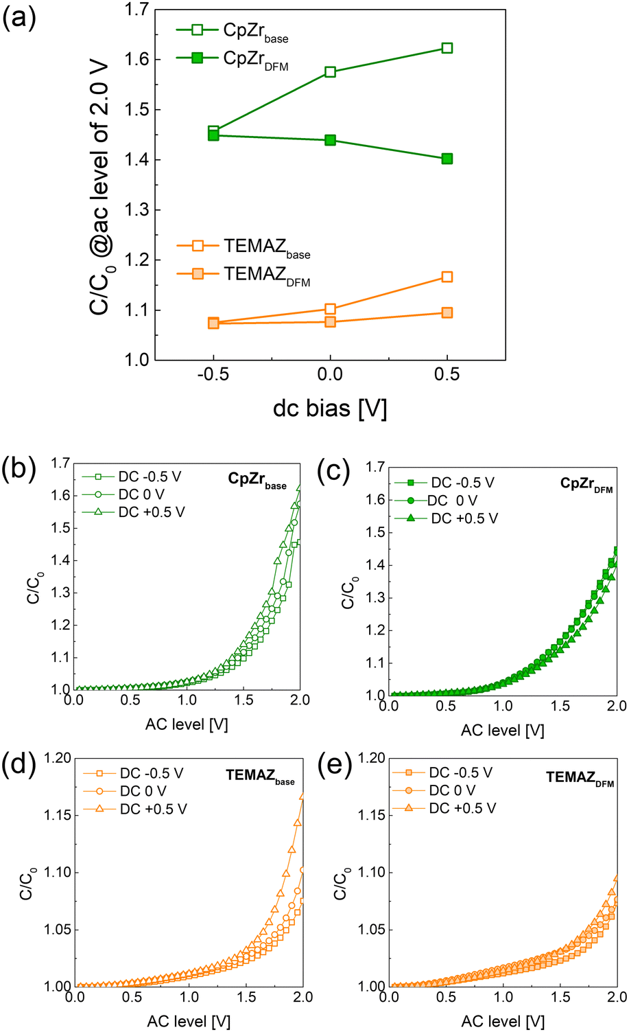 | ||
| Fig. 5 (a) Relative capacitance density (C/C0, where C0 denotes the capacitance at the AC level of 0 V) at the AC level of 2.0 V with respect to the DC bias varied by employing precursors and sequences; C/C0vs. AC level plot with DC bias of −0.5, 0, and 0.5 V for (b) CpZrbase, (c) CpZrDFM, (d) TEMAZbase, and (e) TEMAZDFM. The thickness of ZrO2 was 10 nm for all samples. | ||
Furthermore, the frequency dependence behaviors were examined in MIM capacitors with base and DFM ZrO2 using TEMAZ and CpZr (Fig. 6) with thickness of 10 nm. As the frequency of the AC bias was increased, C/C1k (C1k denotes the capacitance at an AC frequency of 1 kHz) decreased in the MIM capacitors owing to defects in the bulk region of the insulator.20,21 As the frequency increased, the contribution of defects, VO in this case, to the capacitance decreased, thereby resulting in a relatively high decrease in C/C1k depending on the frequency. In the C/C1kvs. frequency (C/C1k–freq.) curve, the ZrO2 thin film-deposited CpZrDFM and TEMAZDFM sequences exhibited improved properties compared with those of CpZrbase and TEMAZbase. Furthermore, the improvement in C/C0-freq. was significantly higher in the TEMAZ case than in the CpZr case, which coincided with an increase in film density. The above results confirm that the cut-in purge removed the screening effect of the physisorbed ligands and impurities bonded to the Zr atoms, thereby enhancing the film density. If the deposited thin film contains numerous impurities, the impurities bonded to the Zr atoms are removed via thermal treatment, thereby generating oxygen defects in the ZrO2 thin film,23 eventually, resulting in increasing the frequency dependence of the insulator and the capacitance loss. This implies that the bulk defects in the ZrO2 thin film can be reduced using the DFM, and the density of ZrO2 deposited with TEMAZ, which had a higher cut-in purge effect than CpZr, was improved, and the frequency dependency was reduced.
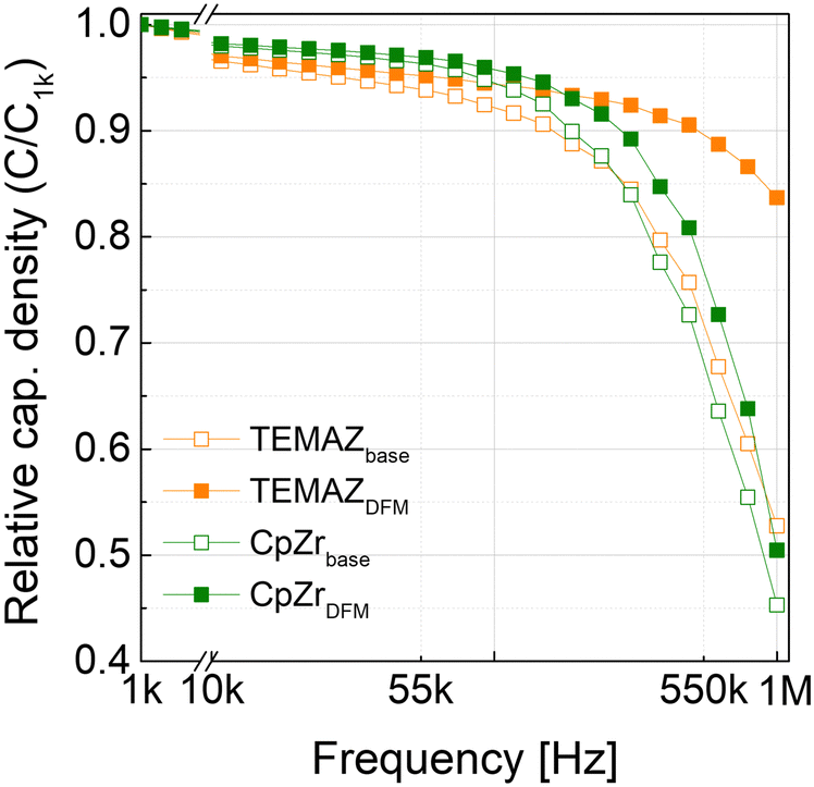 | ||
| Fig. 6 Relative capacitance density (C/C1k, where C1k denotes the capacitance at a frequency of 1 kHz) vs. frequency for the ZrO2 thin films with a thickness of 10 nm. | ||
The crystal structures of the 10 nm-thick base and DFM ZrO2 were evaluated using XRD analysis (Fig. 7(a)). Note that the tetragonal phase of ZrO2 is thermodynamically stable without doping in ALD-deposited thin films.24 Therefore, the base and DFM ZrO2 of both precursors crystallized in the tetragonal phase almost identically, without any significant difference. In this regard, the change in capacitance density depending on the ALD sequence was almost negligible. As shown in Fig. 7(b), the capacitance density was slightly increased by employing DFM for both precursors, which is almost negligible compared with the previous results. In contrast to the capacitance density change, the leakage current density (J) dramatically changed depending on the ALD sequence. Moreover, the TEMAZDFM case exhibited improved properties compared with those of CpZrDFM, which coincided with the previous results. In the MIM capacitor employing ZrO2 as the insulator, J is governed by trap-assisted tunneling and Poole–Frenkel emission mechanisms.7,20,24,25 These two mechanisms are strongly related to the defects incorporated in ZrO2. Therefore, TEMAZDFM exhibited significantly improved J characteristics owing to the suppression of interfacial layer formation of TiN/ZrO2 and VO in the bulk region. However, in the CpZrDFM case, J was slightly decreased when a positive bias, where the electron injected from the bottom electrode, was applied, thus implying a relatively small improvement on the interface in the CpZrDFM sequence. The enhancement in J increased with decreasing physical thickness of the ZrO2 film because the ratio of the interface in the entire MIM structure increased (Fig. 7(d)). In addition, the enhancement of J with decreasing film thickness was more strongly related in the TEMAZDFM case than in the CpZrDFM case. Consequently, scaling of the equivalent oxide thickness (tox) was significantly enhanced. In the J–tox plot (Fig. 7(d)), the tox change between the base and DFM sequences was insignificant because of the small change in the k value. However, the J value was decreased by employing DFM, thus inducing scaling on the tox.
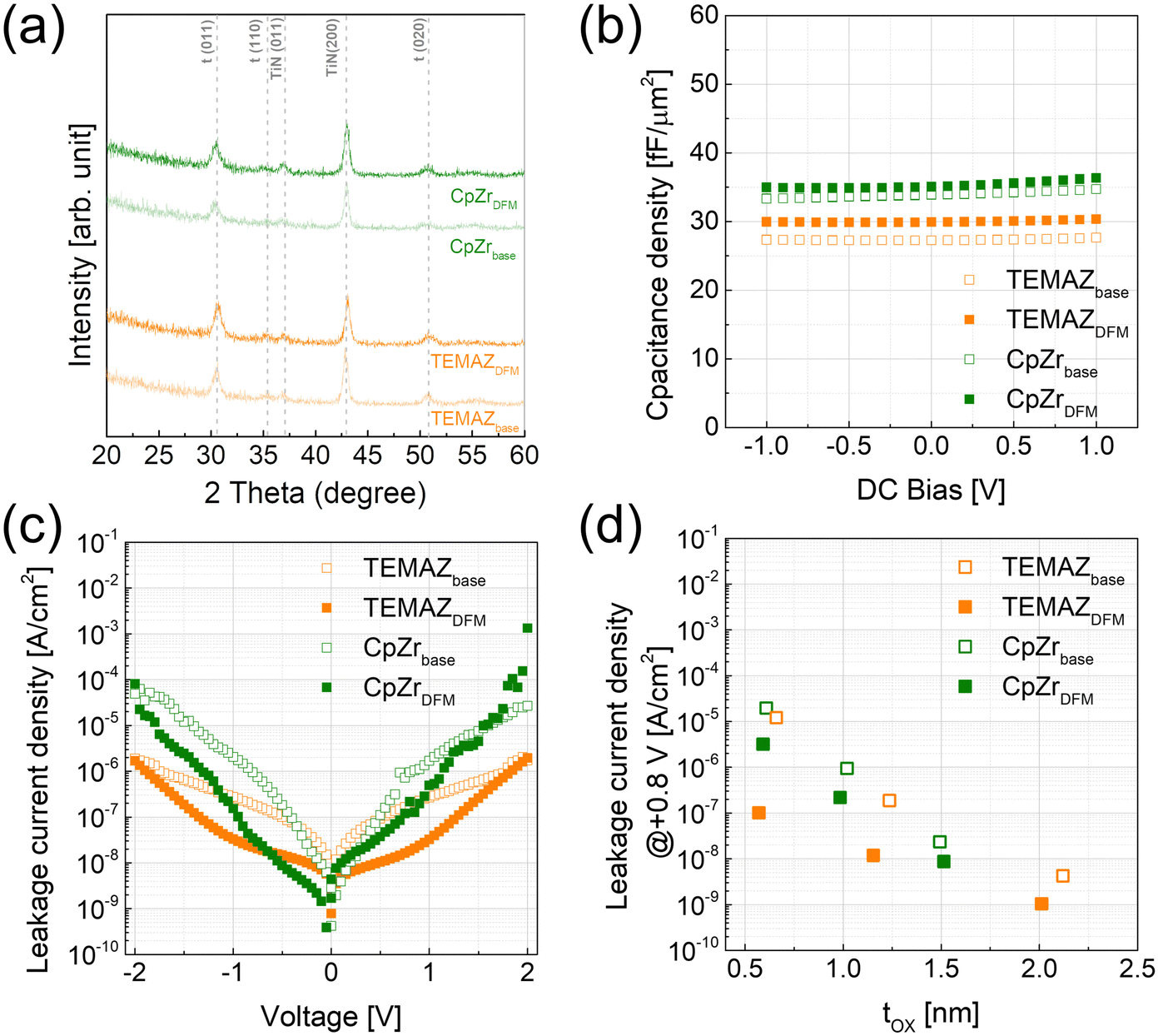 | ||
| Fig. 7 (a) XRD patterns, (b) capacitance density vs. DC bias curves, and (c) leakage current density vs. applied bias curves for the 10 nm-thick-ZrO2 thin films; and (d) J–tox plot for the ZrO2 thin films for varied physical thickness. | ||
Conclusions
The interfacial layer formation between electrodes and insulators originating from the oxidation step during insulator deposition by employing the ALD process was thoroughly investigated. The analyses revealed that the damage to the surface of the electrode, generally in unintended oxidation, can be attributed to the exposure of the surface of the electrode to the oxidant due to the screening effect of the physisorbed precursor as well as the steric hindrance effect of the ligand. Consequently, the elimination of the screening effect by employing the DFM effectively suppressed interfacial layer formation, thereby resulting in a significant improvement in the electrical properties of a MIM capacitor. This result indicates that suppressing the interfacial layer formation becomes more important as the physical thickness of insulators in MIM capacitors decreases; thus, suppressing the interfacial layer formation by employing the DFM is the most effective method to develop next-generation DRAM capacitors.Author contributions
The manuscript was written through contributions of all authors. All authors have given approval to the final version of the manuscript. A. J. Lee, S. Lee, and D. H. Han performed thin film deposition, device fabrication, and characterization. S. Lee, and Y. Kim carried out device fabrication. A. J. Lee performed chemical analyses. Y. Kim, and W. Jeon designed the experiment and co-wrote the paper. All of the authors discussed the results and commented on the paper.Conflicts of interest
There are no conflicts to declare.Acknowledgements
This work was supported by the Technology Innovation Program (No. 20017832 and 20019394) funded by the Ministry of Trade, Industry & Energy (MOTIE, Korea), the Basic Science Research Capacity Enhancement Project through Korea Basic Science Institute (National research Facilities and Equipment Center) grant funded by the Ministry of Education. (No. 2019R1A6C1010052), and the Korea Institute of Energy Technology Evaluation and Planning (KETEP) grant funded by the Korean government (MOTIE) (20201520300140, Development of Advanced Functional Material with C-14 from PHWR Waste). W. Jeon would like to acknowledge the support provided by SK Trichem Inc. for supplying the precursors used in this study.References
- T. Ando, Materials, 2012, 5, 478–500 CrossRef CAS PubMed.
- M. Ritala, K. Kukli, A. Rahtu, P. I. Räisänen, M. Leskelä, T. Sajavaara and J. Keinonen, Science, 2000, 288, 319–321 CrossRef CAS PubMed.
- M. Bhuyian, D. Misra, K. Tapily, R. Clark, S. Consiglio, C. Wajda, G. Nakamura and G. Leusink, ECS Trans., 2013, 58, 17–29 CrossRef.
- H. Lim, G. Cho and H. Jung, Adv. Mater. Technol., 2022, 2200412, 1–8 Search PubMed.
- J. H. Lee, B. E. Park, D. Thompson, M. Choe, Z. Lee, I. K. Oh, W. H. Kim and H. Kim, Thin Solid Films, 2020, 701, 137950 CrossRef CAS.
- S. K. Kim and C. S. Hwang, Electrochem. Solid-State Lett., 2008, 11, 9–12 CrossRef.
- W. Jeon, Y. Kim, C. H. An, C. S. Hwang, P. Gonon and C. Vallee, IEEE Trans. Electron Devices, 2018, 65, 660–666 CAS.
- Y. Kim, S. Y. Kang, J. H. Choi, J. S. Lim, M. Y. Park, S. J. Chung, J. Chung, H. I. Lee, K. H. Kim, Y. K. Kyoung, S. Heo, C. Y. Yoo and H. K. Kang, J. Nanosci. Nanotechnol., 2011, 11, 8309–8312 CrossRef CAS PubMed.
- T. J. Park, J. H. Kim, J. H. Jang, U. K. Kim, S. Y. Lee, J. Lee, H. S. Jung and C. S. Hwang, Chem. Mater., 2011, 23, 1654–1658 CrossRef CAS.
- Y. Cho, S. H. Kim, B. S. Kim, Y. Kim and W. Jeon, Phys. Chem. Chem. Phys., 2021, 23, 2568–2574 RSC.
- J. W. Han, H. S. Jin, Y. J. Kim, J. S. Heo, W. H. Kim, J. H. Ahn, J. H. Kim and T. J. Park, Nano Lett., 2022, 22, 4589–4595 CrossRef CAS PubMed.
- D. S. Kwon, W. Jeon, D. G. Kim, T. K. Kim, H. Seo, J. Lim and C. S. Hwang, ACS Appl. Mater. Interfaces, 2021, 13, 23915–23927 CrossRef CAS PubMed.
- J. C. Park, C. I. Choi, S. G. Lee, S. J. Yoo, J. H. Lee, J. H. Jang, W. H. Kim, J. H. Ahn, J. H. Kim and T. J. Park, J. Mater. Chem. C, 2023, 11, 1298–1303 RSC.
- H. Song, D. Shin, J. E. Jeong, H. Park and D. H. Ko, AIP Adv., 2019, 9, 035333 CrossRef.
- S. Park, B. E. Park, H. Yoon, S. Lee, T. Nam, T. Cheon, S. H. Kim, H. Cheon, S. Im, T. Seong and H. Kim, J. Mater. Chem. C, 2020, 8, 1344–1352 RSC.
- J.-M. Lee, J. Lee, J. W. Han, H. Park, S. Kyung, I. W. Kim, J. M. Lee, T. J. Park and W.-H. Kim, Appl. Surf. Sci., 2021, 539, 148247 CrossRef CAS.
- J. Yu, J. Yu, J. Yu, P. Phang, C. Samundsett, R. Basnet, G. P. Neupan, X. Yang, D. H. Macdonald, Y. Wan, D. Yan and J. Ye, ACS Appl. Mater. Interfaces, 2020, 12, 26177–26183 CrossRef CAS PubMed.
- E. O. Filatova, S. S. Sakhonenkov, A. S. Konashuk and V. V. Afanas’Ev, Phys. Chem. Chem. Phys., 2018, 20, 27975–27982 RSC.
- A. Paskaleva, M. Lemberger, A. J. Bauer, W. Weinreich, J. Heitmann, E. Erben, U. Schröder and L. Oberbeck, J. Appl. Phys., 2009, 106, 054107 CrossRef.
- D. H. Han, S. Lee, J. H. Hwang, Y. Kim, M. Bonvalot, C. Vallee, P. Gonon and W. Jeon, IEEE Trans. Electron Devices, 2021, 68, 5753–5757 CAS.
- O. Khaldi, F. Jomni, P. Gonon and C. Vallée, J. Mater. Sci.: Mater. Electron., 2020, 31, 19036–19043 CrossRef.
- K. D. Fredrickson, M. D. McDaniel, A. Slepko, J. G. Ekerdt and A. A. Demkov, J. Chem. Phys., 2016, 145, 064701 CrossRef.
- D.-Y. Cho, H. S. Jung, I.-H. Yu, J. H. Yoon, H. K. Kim, S. Y. Lee, S. H. Jeon, S. Han, J. H. Kim, T. J. Park, B.-G. Park and C. S. Hwang, Chem. Mater., 2012, 24, 3534–3543 CrossRef CAS.
- W. Weinreich, A. Shariq, K. Seidel, J. Sundqvist, A. Paskaleva, M. Lemberger and A. J. Bauer, J. Vac. Sci. Technol., B: Nanotechnol. Microelectron.: Mater., Process., Meas., Phenom., 2013, 31, 01A109 Search PubMed.
- W. Jeon, J. Mater. Res., 2020, 35, 775–794 CrossRef CAS.
Footnote |
| † Electronic supplementary information (ESI) available. See DOI: https://doi.org/10.1039/d3tc00704a |
| This journal is © The Royal Society of Chemistry 2023 |