
 Open Access Article
 This Open Access Article is licensed under a Creative Commons Attribution-Non Commercial 3.0 Unported Licence
AlGaN-based solar-blind UV heterojunction bipolar phototransistors: structural design, epitaxial growth, and optoelectric properties†
Yiren
Chen
 *a,
Jiawang
Shi
ab,
Zhiwei
Zhang
a,
Guoqing
Miao
a,
Hong
Jiang
a and
Hang
Song
*a
*a,
Jiawang
Shi
ab,
Zhiwei
Zhang
a,
Guoqing
Miao
a,
Hong
Jiang
a and
Hang
Song
*a
aState Key Laboratory of Luminescence and Applications, Changchun Institute of Optics, Fine Mechanics and Physics, Chinese Academy of Sciences, Changchun 130033, China. E-mail: chenyr@ciomp.ac.cn; songh@ciomp.ac.cn
bSchool of Optoelectronics, University of Chinese Academy of Sciences, Beijing 100049, China
First published on 15th May 2023
Abstract
An AlGaN-based solar-blind UV heterojunction bipolar phototransistor (HBPT) with an AlGaN-based multiple quantum well (MQW) layer as the light absorption layer is proposed in this paper. On the basis of the individually optimized growth of the MQW light absorption layer and the p-type AlGaN base layer, the material growth, device preparation, and performance evaluation of the solar-blind UV HBPT are investigated in detail. The evaluations show that the fabricated two-end NPN-type phototransistor with a floating base presents a low dark current density of about 4.8 × 10⁻⁸ A cm−2 and a high peak responsivity of 4.55 A W−1 at 267 nm as the device is biased at a VCE of 12 V, corresponding to a high EQE of 2.1 × 10³%. It also exhibits a quick transient response speed of 13.47 ns at a lower bias voltage (VCE = 3 V). These results favorably prove the feasibility of realizing a high performance solar-blind UV photodetector based on the AlGaN-based MQW HBPT.
1. Introduction
Compared with visible and infrared photodetectors, solar-blind ultraviolet (UV) photodetectors working in the spectral region of 200–280 nm are less interfered by the background noise of the sun, and can be used to realize efficient and accurate detection of ultraviolet radiation from unnatural factors. Thus, this type of detector has widespread application prospects and a huge potential market demand in military and civil fields.1–3In the military field, one of the core applications of solar-blind UV photodetectors is missile approaching warning.4 As is well known, in modern warfare, missiles are mainly used to attack the strategic targets that determine the victory or defeat of a war and even the survival of a country. Thus, the accurate and effective warning of incoming missiles appears to be crucial. Missiles mainly propelled by solid or liquid fuels can produce UV radiation in the process of flying, originating from three sources: (i) the unburned solid fuel particles in the exhaust plume of the missiles during flight will mix with the air outside the engine and secondary combustion occurs, resulting in high temperature particle radiation.5 (ii) The chemical luminescence caused by CO–O recombination will also be emitted during the secondary combustion of unburned fuel.6 (iii) The skin of the missile rigging and tank emits UV radiation by friction with the atmosphere during the reentry segment.4 Both of the high temperature particle radiation and the chemical luminescence contain strong solar-blind UV components.7,8 Therefore, the solar-blind UV radiation in the missile exhaust plume detected using the corresponding solar-blind UV photodetectors can realize the approaching alarm of incoming missiles with a very low false alarm rate, which ensures the security of important strategic targets in the environment of precise attack war. In the civil field, there is also a huge market demand for solar-blind UV photodetectors in corona detection and inspection of (ultra) high voltage power grids.9 Since the radiation of the leakage corona of (ultra) high voltage transmission lines is mainly concentrated in the solar-blind UV band, using solar-blind UV photodetectors to detect the radiation of discharge corona can not only realize real-time monitoring day and night against the operation status of (ultra) high voltage transmission lines, but also implement troubleshooting and maintenance timely and accurately. It is of great significance for ensuring the operation safety of national high voltage power grids, preserving the economic development and people's normal life order, and guaranteeing the sustainable development of the national energy strategy.
Although the application prospect of a solar-blind UV photodetector is attractive, its development still faces many crucial problems. Typically, the energy of solar blind UV photons is larger than that of visible and infrared photons, which means that the number of solar blind UV photons is much less than that of visible and infrared photons under the same irradiation power. Moreover, the combination of scattering and absorption due to the interaction between the solar-blind UV photons and the molecules and suspended particles in the atmosphere makes the solar-blind UV signal to rapidly attenuate.10 These factors pose a serious challenge to the sensitivity of solar-blind UV photodetectors. Only the detectors with high gain and low noise can meet the detection requirements of the extremely weak solar-blind UV signal. The conventionally used high gain solar-blind UV photodetectors are mainly photocathode-based photomultiplier tubes (PMTs)11 or photomultiplication type organic photodetectors.12,13 Although both have the advantages of high gain and low noise, their broadband response characteristics lead to the fact that in order to achieve sheer solar-blind UV detection, it must rely on high cutoff ratio solar-blind UV bandpass filters, and the detection ability is thus seriously restrained by the transmittance of the filter.3,14
In order to get rid of the dependence on filters, researchers concentrate on developing solar-blind UV photodetectors with an intrinsic cut-off response spectrum. Nitride semiconductors have the potential to solve the above-mentioned issues. Since the direct bandgap of AlGaN ternary alloy ranges from 3.4 to 6.2 eV at room temperature, and the corresponding spectrum ranges from 200 nm to 365 nm, it is suitable for developing solar-blind UV photosensors by adjusting the Al content.2,15 Furthermore, it can be used for developing full solid-state, durable, low-cost and high UV/visible rejection ratio solar-blind UV photodetectors due to its excellent physical and chemical properties.16 Revolving around the research of gain-type, full-solid AlGaN-based solar-blind UV photodetectors, avalanche photodiodes (APDs) based on a separate absorption and multiplication (SAM) structure have attracted much attention and the gain of AlGaN APDs can reach an order of 103 to date.17,18 Apart from the SAM structure APDs, phototransistors in the form of the AlGaN heterojunction high electron mobility transistors (HEMTs) are also proposed as gain-type solar-blind UV photodetectors to achieve high gains.15,19,20 However, the fabrication of gain-type solar-blind UV photodetectors based on the heterojunction bipolar phototransistor (HBPT) is still a big challenge. The reasons can be attributed to the following two points. On the one hand, it is difficult to obtain high performance p-AlGaN with a high Al content. For bipolar phototransistors, no matter NPN type or PNP type, p-type materials are indispensable. However, the development of AlGaN-based short-wavelength optoelectronic devices has been seriously limited by p-type materials for the reason that high activation energy leads to very low p-type doping efficiency of AlGaN with a high Al content, because of the strong localization of the acceptors making them become deep level dopants.21,22 On the other hand, low photoelectric conversion efficiency resulting from the weak light absorption capacity of the PN junction cannot provide sufficient base injection current for conventional NPN or PNP type bipolar phototransistors.
Herein, we propose an NPN type solar-blind UV HBPT device structure with AlGaN-based multiple quantum wells (MQWs) as the optical absorption region and a superlattice structure material with the alternate Mg uniformly doped layer and Mg-delta doped layer as the p-type material. The introduction of AlGaN-based MQWs instead of ordinary intrinsic AlGaN single layers into the PN junction to achieve photoelectric conversion has the advantage of high quantum efficiency, which plays an important role in solving the problem of the weak light absorption capacity of the PN junction. An effective way of the non-equilibrium Mg doping method is adopted to solve the low doping efficiency of p-AlGaN and to improve its electrical performance. Accompanied by the individual optimized growth of the MQW optical absorption layer and the p-type layer via metal–organic chemical vapor deposition (MOCVD), the full structural material of an NPN type solar-blind UV HBPT equipped with an AlGaN-based MQW optical absorption layer is grown, and finally, the performance of the solar-blind UV HBPT is carefully evaluated after device preparation. The results reveal the feasibility of realizing high gain solar-blind UV photodetectors based on the AlGaN-based NPN type HBPT with the MQW optical absorption region.
2. Experimental
2.1 Structure design of the solar-blind UV HBPT
Referring to the structure of Si-based heterojunction phototransistors,23 the solar-blind UV HBPT based on the AlGaN-based NPN structure is proposed, in which the AlGaN-based MQW absorption layer is introduced between the base (B) and the collector (C). The MQWs will play the role of increasing the light absorption in comparison with the depletion region in the PN junction. The schematic band diagram of the proposed structure is shown in Fig. 1. Under light exposure from the collector (C) side, the MQWs in the base-collector region absorb incident light energy, creating photo-induced electrons and holes. In the case of the base open configuration and operating in the amplification mode (VBE > 0 and VCB > 0), the photo-generated electrons will be swept to the collector (C) as part of the initial photocurrent of the HBPT. In the meantime, the photo-generated holes will diffuse to the base (B) region and inject into the emitter (E) via lowering the energy barrier of the base-emitter. The barrier lowering enables a large number of electrons in the emitter (E) to diffuse across the base (B) to the collector (C), finally realizing initial photocurrent magnification.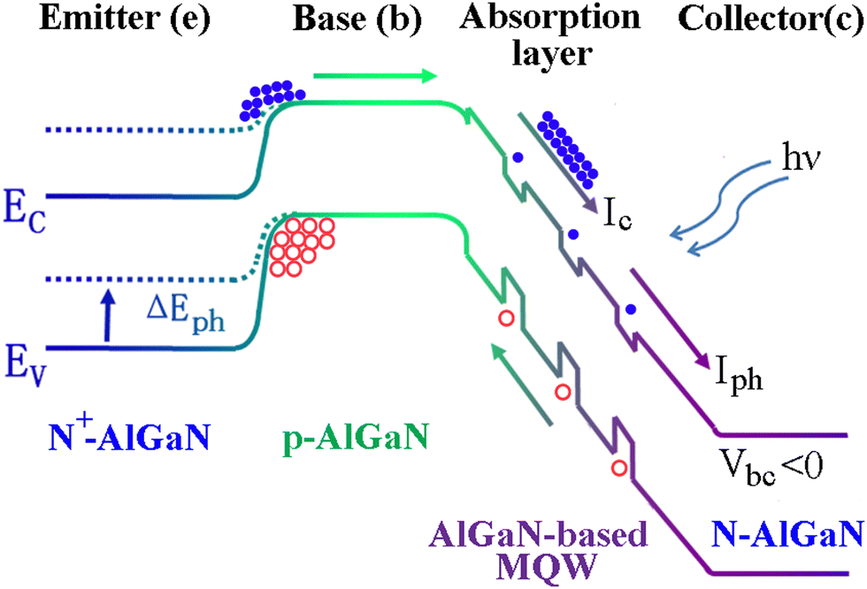 | ||
| Fig. 1 Schematic band diagram of the proposed NPN type solar-blind UV HBPT with the AlGaN-based MQW absorption layer. | ||
2.2 The optimized growth of AlGaN-based MQWs
Based on the above structural design and analysis, the individually optimized growth of AlGaN-based MQWs for the solar-blind UV HBPT was carried out at first. Two kinds of MQW structures shown in the inset of Fig. 2 were used for the comparative study. Both MQW structures were grown on 2-inch pre-grown AlN templates by low-pressure MOCVD. The detailed preparation of the AlN templates could be referred to our previous article.14 During growth, trimethylaluminum (TMAl), trimethylgallium (TMGa), and ammonia (NH3) were used as aluminium, gallium, and nitrogen sources, respectively, and hydrogen (H2) was used as the carrier gas. Prior to the growth of five periods Al0.45Ga0.55N/AlN (4 nm/10 nm) MQWs or Al0.45Ga0.55N/Al0.5Ga0.5N (4 nm/10 nm) MQWs, a 500 nm-thick unintentional doped Al0.5Ga0.5N layer (i-Al0.5Ga0.5N) was deposited on the AlN template as a buffer layer. For Al0.45Ga0.55N/AlN MQWs, it was grown at a uniform temperature of 1200 °C by periodically adjusting the Ga source on/off and continuously supplying Al and N sources. For Al0.45Ga0.55N/Al0.5Ga0.5N MQWs, it was prepared by growth temperature modulation under constant TMAl, TMGa, and NH3 source flows. The growth temperatures of the Al0.45Ga0.55N well and Al0.5Ga0.5N barrier were 1160 °C and 1200 °C, respectively.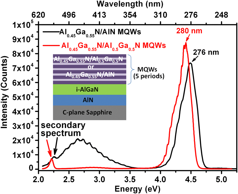 | ||
| Fig. 2 PL spectra of both Al0.45Ga0.55N/AlN MQWs and Al0.45Ga0.55N/Al0.5Ga0.5N MQWs. The inset shows their epitaxial structures. | ||
2.3 The optimized growth of the p-type doping AlGaN material
Two p-type AlGaN materials were respectively obtained by single uniform doping of magnesium and the combination of uniform doping and delta (δ) doping of magnesium for a comparative study. The structures of the two samples are shown in Fig. S1(a) and S2(a) of the ESI,† respectively. The growth was carried out on two c-plane sapphire substrates using TMAl, TMGa, and NH3 as Al, Ga, and N precursors, and dicyclopentadienyl magnesium (Cp2Mg) as the p-type dopant. During growth, both substrates epitaxially grew a 700 nm-thick AlN layer, followed by a 500 nm-thick unintentional doped Al0.45Ga0.55N layer (i-Al0.45Ga0.55N) as the buffer layer. One p-type Al0.35Ga0.65N (Fig. S1(a), ESI†) with a thickness of 500 nm was deposited on the buffer layer by uniform magnesium doping which was continuously injecting the Mg dopant into the reaction chamber during AlGaN growth. The corresponding asymmetrical reciprocal space mapping (RSM) around the (10![[1 with combining macron]](https://www.rsc.org/images/entities/char_0031_0304.gif) 5) reflection is shown in Fig. S1(b) (ESI†), which was quite in agreement with the growth structure. The other one (Fig. S2(a), ESI†) was obtained by the periodic growth process containing twenty cycles, each consisting of three successive steps, the uniform magnesium doping in Al0.35Ga0.65N, the short-time magnesium doping in GaN and the short-time magnesium injecting (Mg-δ doping). The detailed implementation strategy was maintaining the N source supply, opening the Al, Ga, and Mg sources simultaneously for a 20 nm-thick Mg-doped Al0.35Ga0.65N growth, then turning off the Al source for 20 s for an Mg-doped GaN growth, and finally turning off the Ga source and maintaining the Mg source supply for 20 s. In this way, one cycle of p-type material growth was completed. The corresponding asymmetrical RSM around the (105) reflection is shown in Fig. S2(b) (ESI†). As could be seen, in addition to the reciprocal space lattices of AlN and i-Al0.45Ga0.55N layers, the periodic material structure formed the diffraction pattern of superlattices. Both samples were rapidly annealed at 850 °C under a N2 atmosphere to activate the Mg dopants.
5) reflection is shown in Fig. S1(b) (ESI†), which was quite in agreement with the growth structure. The other one (Fig. S2(a), ESI†) was obtained by the periodic growth process containing twenty cycles, each consisting of three successive steps, the uniform magnesium doping in Al0.35Ga0.65N, the short-time magnesium doping in GaN and the short-time magnesium injecting (Mg-δ doping). The detailed implementation strategy was maintaining the N source supply, opening the Al, Ga, and Mg sources simultaneously for a 20 nm-thick Mg-doped Al0.35Ga0.65N growth, then turning off the Al source for 20 s for an Mg-doped GaN growth, and finally turning off the Ga source and maintaining the Mg source supply for 20 s. In this way, one cycle of p-type material growth was completed. The corresponding asymmetrical RSM around the (105) reflection is shown in Fig. S2(b) (ESI†). As could be seen, in addition to the reciprocal space lattices of AlN and i-Al0.45Ga0.55N layers, the periodic material structure formed the diffraction pattern of superlattices. Both samples were rapidly annealed at 850 °C under a N2 atmosphere to activate the Mg dopants.
2.4 The structural material preparation of the solar-blind UV HBPT
On the basis of the optimized growth of the light absorption layer and the p-type AlGaN material, the full structure and in situ growth monitoring curves of the AlGaN-based solar-blind UV HBPT are demonstrated in Fig. 3(a) and (b). The HBPT structural material was directly grown on an AlN template (with full width at half maximum (FWHM) values of (0002) and (102) planes about 89 arcsec and 860 arcsec, respectively, as shown in Fig. S3 of the ESI†) in a sequence of ten periods of Al0.6Ga0.4N/AlN (6 nm/6 nm) superlattices (SLs), a 240 nm-thick unintentional doped Al0.6Ga0.4N layer, a 400 nm-thick Si-doped n-Al0.49Ga0.51N layer with a low electron concentration of 3.7 × 1017 cm−3 (collector), five periods of Al0.45Ga0.55N/Al0.5Ga0.5N (4 nm/10 nm) MQWs, a periodic uniform Mg doping and Mg-δ doping p-type Al0.35Ga0.65N with a total thickness of 60 nm (base), and a 600 nm-thick Si-doped n+-Al0.49Ga0.51N layer with a high electron concentration of 6.8 × 1018 cm−3 (emitter). The whole epitaxial material was in situ annealed in the MOCVD chamber under a N2 atmosphere for 30 min.
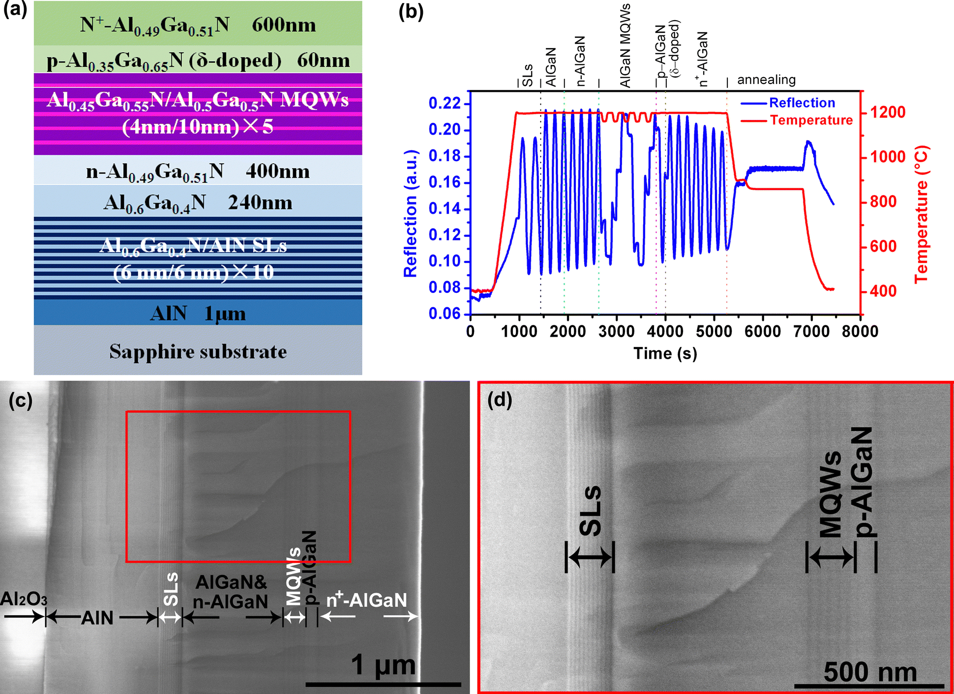 | ||
| Fig. 3 (a) The epitaxial structure of the AlGaN-based solar-blind UV HBPT. (b) The recorded reflectance and growth temperature curves vs. time during epitaxial growth. (c) Cross-sectional SEM images of the AlGaN-based solar-blind UV HBPT material. (d) Partial enlargement image of (c). | ||
2.5 Characterization
The photoluminescence (PL) spectrum was recorded using a spectrophotometer using a 50 mW 213 nm-wavelength Nd:YAG laser as the excitation source. The 405 nm in situ optical monitoring system (LayTec AG) was used to record the information such as reflectance and growth temperature during the growth process. The asymmetrical RSM around the (105) reflection was obtained using a high-resolution X-ray diffractometer (HRXRD, Bruker D8). The electrical characteristics of the AlGaN-based solar-blind UV HBPT were measured using a semiconductor parameter analyzer (Agilent B1500A). The carrier concentrations in the p-type AlGaN samples were evaluated using a Hall testing system (Lake Shore 8400 series). The spectral characteristics including the responsivity and external quantum efficiency (EQE) of the AlGaN-based solar-blind UV HBPT were measured using an ultraviolet spectral response test system equipped with a UV-enhanced Si-based photodetector as the calibration. The transient response spectrum of the HBPT was timely captured using a digital oscilloscope (Tektronix DPO 5104), which was stimulated using a 10 mW 266 nm-wavelength Nd:YAG laser.
2.6 Device fabrication
Prior to a standard photolithography process, the AlGaN-based solar-blind UV HBPT material was rapidly annealed at 850 °C under a N2 atmosphere for the purpose of activating the Mg dopants in the p-type layer. Subsequently, the standard microelectronic processes such as depositing the SiO2 dielectric mask, photolithography and inductively-coupled plasma (ICP) etching were adopted to etch the material to the n-Al0.49Ga0.51N (collector), leaving a 500 μm-diameter circle mesa. Then, a circle electrode located on top of the mesa and a ring-like electrode surrounding the mesa based on Ti/Al/Ni/Au (50 nm/100 nm/120 nm/200 nm) multilayer metallic films were simultaneously fabricated by electron beam evaporation and the lift-off process. Finally, the whole device was rapidly annealed at 700 °C for 60 s under a N2 atmosphere to realize the Ohmic contact and thus a two-terminal phototransistor was fulfilled.3. Results and discussion
Based on the designed structure of the AlGaN-based solar-blind UV HBPT (Fig. 1), two elements, viz. the MQW optical absorption layer and the p-type layer, are firstly implemented for optimal growth. Fig. 2 shows the PL spectra of both Al0.45Ga0.55N/AlN MQWs and Al0.45Ga0.55N/Al0.5Ga0.5N MQWs for a comparative study. As can be seen, the main PL peaks of Al0.45Ga0.55N/AlN MQWs and Al0.45Ga0.55N/Al0.5Ga0.5N MQWs are respectively located at 4.49 eV and 4.42 eV. It should be noted that the slight difference in the peak position is originated from the fluctuation of the Al content during growth. In addition to the main peak, both PL spectra exhibit a weak secondary spectrum. Fabry–Perot fringes are visible in both spectra due to the smooth surface and the interface between the film and the substrate. However, the reductive luminescence in the energy range between 2.0 eV and 3.5 eV for the PL spectrum of Al0.45Ga0.55N/Al0.5Ga0.5N MQWs indicates a reduction of point defects incorporated into the film during growth. The emissions in this energy range have been identified as originating from the conduction band to the deep acceptor state transition such as cation vacancy, cation vacancy complexes, and/or carbon.24–27 Moreover, by comparing the intensity of the PL luminescence under the same excitation light power, it is determined that using the Al0.5Ga0.5N barrier results in a high internal quantum efficiency (IQE) value, which indicates that the use of a narrower bandgap barrier facilitates to improve the electron and hole injection into the active region or extraction from the active region.28 It can be said that more efficient MQW optical absorption layers can be obtained by the regulation of the barrier bandgap. Herein, Al0.45Ga0.55N/Al0.5Ga0.5N MQWs are preferred as the optical absorption layer for the AlGaN-based solar-blind UV HBPT.With regard to the p-type layer as the base of the HBPT, optimized growth is also carried out using single uniform Mg doping and the combination of uniform Mg doping and Mg-δ doping for comparison. After evaluating the Hall effect measurement, the results shown in Table S1 of the ESI† demonstrate that the carrier concentration and the hole mobility of the uniform Mg-doping sample cannot be measured due to its high impedance while those of periodic uniform Mg doping and Mg-δ doping samples are 2.16 × 1018 cm−3 and 0.4602 cm2 V−1 s−1, respectively. The electrical properties of the p-type AlGaN material are greatly improved in the periodic uniform Mg doping and Mg-δ doping samples, mainly originating from the non-equilibrium superlattice doping technique. As demonstrated in the Experimental section, the periodic uniform Mg doping and Mg-δ doping samples have a typical superlattice structure. It is verified that the vertical miniband transport of holes occurs in the p-type AlGaN superlattices, which significantly reduces the effective activation energy of Mg dopants.21 Meanwhile, the ultrathin Mg-δ layer plays a role of the non-equilibrium doping layer that produces a new band edge and thus further tunes the activation energy.22 Therefore, it is a good choice to use the periodic uniform Mg doping and Mg-δ doping methods to prepare the base of the NPN-type AlGaN-based phototransistor based on the above comparative study.
After obtaining the optimized growth parameters of the optical absorption layer and the base layer, the whole structural material of the designed HBPT (Fig. 3(a)) is implemented by MOCVD. Its corresponding in situ growth monitoring curves are shown in Fig. 3(b), in which the growth begins at the Al0.6Ga0.4N/AlN superlattices (SLs) and ends at annealing at 860 °C for 20 min. As seen in Fig. 3(b), except for the MQW optical absorption layer, the other functional layers use the same growth temperature. The difference of the Al content is realized by regulating the VAl/VGa ratio while the difference of the carrier concentration in n-type materials is realized by regulating the volume flows of the SiH4 dopant. As to the MQW optical absorption layer, it is obtained by the means of controlling the growth temperature. Fig. 3(c) shows the cross-sectional SEM panorama of the AlGaN-based HBPT material which is strictly prepared in accordance with the designed structure in Fig. 1. The typical characteristic layers such as the superlattice layer, multiple quantum layers and adjacent p-type layer can be clearly distinguished. Fig. 3(d) shows the partial enlargement image of the superlattice layer, multiple quantum layers and its adjacent p-type layer, further indicating the consistency between the material growth and the structural design.
Fig. 4(a) shows the schematic configuration and physical image of the as-fabricated AlGaN-based solar-blind UV HBPT. The detailed device preparation process can be referred to the Experimental section above. It is a typical two-end NPN-type phototransistor with a floating base described by the symbol in Fig. 4(a), which differs from the three-end field effect phototransistor.29,30 In the base open configuration, light incident from the sapphire substrate side can be absorbed by the MQW layer interposed in the base-collector region, producing photo-generated electron–hole pairs. Under the combined action of the applied electric field (VCE > 0) and the built-in electric field of the base-collector (both in the same direction), the photo-generated electron–hole pairs will be separated, and the electrons in them will be swept to the collector (C) as part of the initial photocurrent of the HBPT. Meanwhile, the holes will be driven towards the base (B) and trapped in the floating base (B) region.31 The accumulation of excess holes reduces the energy barrier of the emitter junction, enabling a large number of electrons in the emitter (E) to diffuse across the emitter junction to the collector (C), finally realizing a significant increase of the collector photocurrent (ICPh). Fig. 4(b) presents the collector photocurrent density curves under different wavelengths of incident light in comparison with the dark current density curve without any illumination. As can be seen, the collector photocurrent density increases steadily with VCE. It is at least two orders of magnitude higher than the dark current density. It should be noted that the current dropping and then rising process in the I–V characteristic can be regarded as the zero offset due to the depletion process of the thin p-AlGaN layer (base) under an applied electric field, light field or their combined action.32
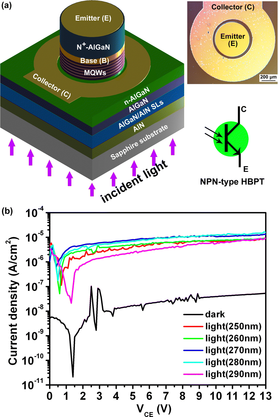 | ||
| Fig. 4 (a) Schematic configuration, physical image and symbol of the NPN-type AlGaN-based HBPT. (b) The I–V characteristic curves of the device measured in the dark and under different illumination wavelengths using a semi-log scale. | ||
The difference of the photocurrent at a certain VCE under different wavelengths of light is originated from the response ability of the AlGaN-based solar-blind HBPT to different wavelengths of light, that is, the different photoelectric conversion efficiency. Fig. 5 shows the measured spectral responsivities and corresponding EQEs (inset) of the AlGaN-based solar-blind HBPT under different bias voltages. At a certain VCE, the spectral responsivity vs. wavelength exhibits a peak value located at around 270 nm. When the VCE is up to 3 V, the peak responsivity reaches 0.266 A W−1 at 267 nm, corresponding to a high EQE of 124%. When the VCE is higher than 3 V, the EQE exceeds 100% for the entire solar-blind UV band, indicating the current amplification in the HBPT. As the VCE further increases, the spectral responsivity and related EQE will further increase. The peak responsivity and EQE can be respectively as high as 4.55 A W−1 and 2.1 × 10³% at 267 nm when the VCE reaches a voltage of 12 V. This VCE-related photoelectric gain in the HBPT has been verified to be determined by the transit time of photogenerated electrons across the base (B) and the lifetime of the excess photogenerated holes trapped in the base (B).31,33 In the open base mode, as the VCE increases, the depletion region of the reverse-biased base-collector junction expands, resulting in the decrease of the neutral base width. The extended depletion region can cooperate with MQWs to absorb more photons and thus produce more photogenerated electrons and holes. At the same time, the narrowing of the base width also results in a significant decrease of the transit time for electrons across the base (B). More excess hole traps in the floating base (B) further reducing the energy barrier of the base-emitter junction that facilitates much more electrons in the emitter (E) across it to the collector (C) and amplifies the initial photocurrent.
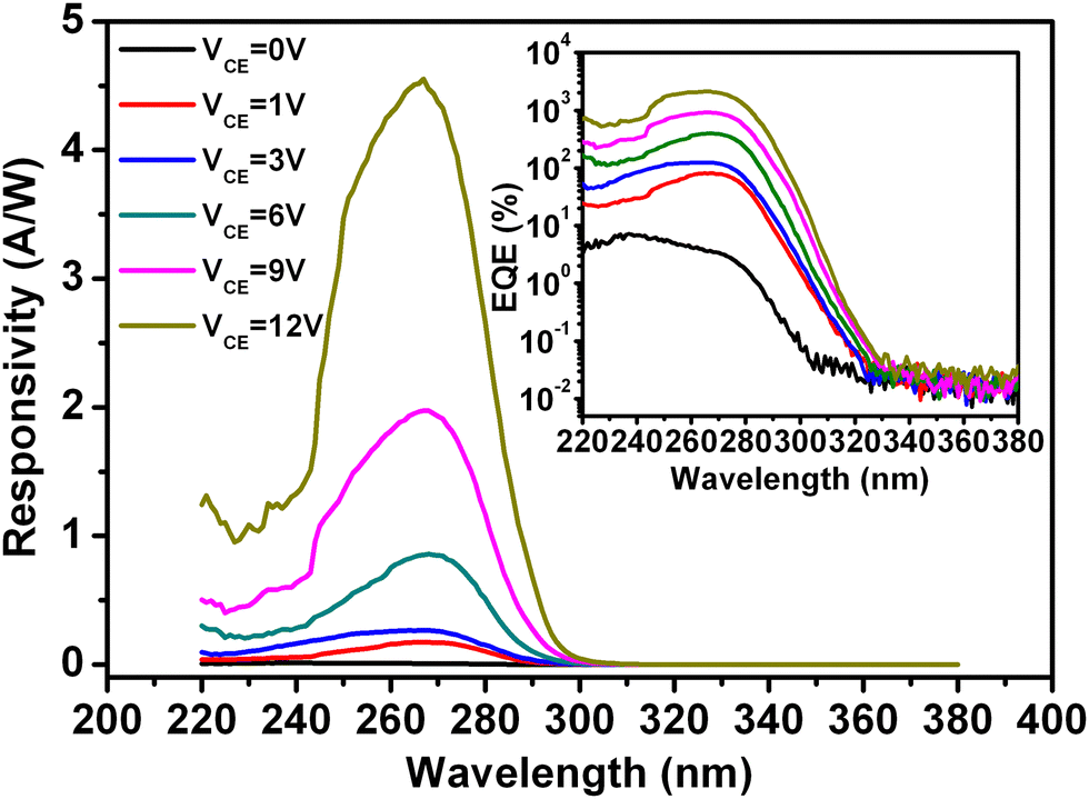 | ||
| Fig. 5 Measured spectral responsivities of the AlGaN-based solar-blind UV HBPT under different biases. The inset shows the corresponding EQE in the semi-log scale. | ||
To further evaluate the performance of our AlGaN-based solar-blind UV HBPT, its transient response is also obtained by the impulse response measurement, as shown in Fig. 6. A 10 mW 266 nm-wavelength pulse laser with a full width at half maximum (FWHM) of 5 ns modulated using a signal generator is coupled through a fiber to the HBPT and a digital sampling oscilloscope timely records the response curve. Fig. 6(a) shows the as-recorded transient response curves, in which the cyan line represents the synchronizing signal of the laser pulse set to a frequency of 10 Hz while the yellow one is on behalf of the temporal response of our HBPT. As can be seen from Fig. 6(b) and (c), the partial enlargement shows a 10–90% rise time of 13.47 ns and a 90–10% decay time of 138.3 ns when the VCE is 3 V, which indicates its relatively good spectral response speed. The different response time at rise and decay processes can be illustrated by the dynamic process of the transient response. AlGaN-based semiconductors are well-known direct bandgap materials. It will absorb the energy of the incident photon higher than its bandgap and directly excite valence band electrons to its conduction band. The electrons in the excited state cannot exist stably, whose energy and momentum will relax towards the minimum value of the valence band (i.e. the base state) soon and eventually release photons again during recombining with the holes. In the process of electrons directly transitioning from the excited state to the base state, it is mainly reflected in very short rise time and decay time. However, generally, the transient response usually presents a slower decay time due to the physical processes such as relaxation, capture and re-release by defect energy levels, and so on.34 In order to intuitively exhibit the comprehensive performance of our AlGaN-based solar-blind UV HBPT, parameter comparison with the reported AlGaN-based solar-blind UV photodetectors is shown in Table 1.
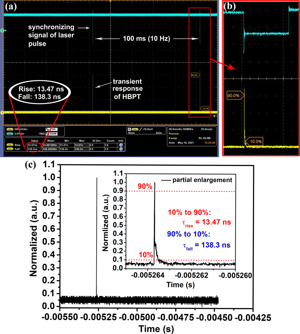 | ||
| Fig. 6 (a) Measured transient spectral response of the AlGaN-based solar-blind UV HBPT. (b) Partial enlargement of (a). (c) Normalized transient spectral response curve. | ||
| Material | Structure | Peak wavelength (nm) | Dark current or dark current density | Responsivity (A W−1) | Rise time/decay time | EQE (%) | Gain-type | Ref. |
|---|---|---|---|---|---|---|---|---|
| AlGaN-based | p–i–n | 275 | <2 × 10⁻⁹ A cm−2 (−10 V) | ∼0.176 (0 V) | — | ∼89 (−5 V) | No | 35 |
| p–i–n | 289 | ∼10−9 A cm−2 (−10 V) | 0.211 (0 V) | — | 92 (0 V) | No | 36 | |
| APD (p–i–n–i–n) | 281 | 1.06 × 10⁻⁸ A cm−2 (−20 V) | ∼2 (−87 V) | — | — | Yes | 37 | |
| p–i–n | ∼271 | 5.89 × 10⁻⁹ A (−5 V) | 0.15 (0 V) | 6.5 ns/τ1 = 67 ns, τ2 = 0.95 μs | 68.8 (0 V) | No | 3 | |
| HBPT (n–i–p–i–n) | ∼285 | 0.8 × 10⁻⁹ A (3 V) | 26.4 (3 V) | — | — | Yes | 31 | |
| MSM | 270 | 0.78 × 10⁻¹² A (−10 V) | 1.84 × 10³ | 90 ms/τ1 = 53 ms, τ2 = 720 ms | — | Yes | 38 | |
| p-MQW-i–n | 233 | ∼10−12 A (<10 V) | 0.425 (0 V) | 224 (0 V) | Yes | 39 | ||
| HBPT (n–p-MQW-n) | ∼267 | ∼4.8 × 10⁻⁸ A cm−2 (12 V) | 4.55 (12 V) | 13.47 ns/138.3 ns | 2.1 × 10³ (12 V) | Yes | This work |
4. Conclusions
In summary, the configuration of an NPN type AlGaN-based solar-blind UV HBPT is designed at first, and then characterization of its material growth, device preparation, and performance is carried out. For improving the optical absorption capacity of the HBPT and thus increasing the injection current to the base (B), the AlGaN-based MQW optical absorption layer is optimally grown as the insertion layer of the base-collector junction. Meanwhile, in order to improve the electrical properties of the base (p-AlGaN), a non-equilibrium superlattice doping method based on periodic uniform Mg doping and Mg-δ doping is used to achieve a high carrier concentration p-AlGaN layer. The fabricated 500 μm-diameter, two-end NPN-type phototransistor with a floating base exhibits a low dark current density of about 4.8 × 10⁻⁸ A cm−2 and a high peak responsivity of 4.55 A W−1 at 267 nm when VCE reaches a voltage of 12 V, corresponding to a high EQE of 2.1 × 10³%, and a transient spectral response of 13.47 ns at a lower bias voltage of 3 V. These results confirm the feasibility of realizing a high performance solar-blind UV photodetector based on the AlGaN-based MQW HBPT.Conflicts of interest
There are no conflicts of interest to declare.Acknowledgements
This work was supported by the Jilin Province Science and Technology Development Plan Item (no. 20230101069JC) and the Independent Project of State Key Laboratory of Luminescence and Applications (no. SKLA-Z-2022-10).References
- U. Varshney, N. Aggarwal and G. Gupta, J. Mater. Chem. C, 2022, 10, 1573–1593 RSC.
- Q. Cai, H. You, H. Guo, J. Wang, B. Liu, Z. Xie, D. Chen, H. Lu, Y. Zheng and R. Zhang, Light: Sci. Appl., 2021, 10, 94 CrossRef CAS PubMed.
- Y. Chen, Z. Zhang, H. Jiang, Z. Li, G. Miao and H. Song, J. Mater. Chem. C, 2018, 6, 4936–4942 RSC.
- D. Yao, W. Hao, X. Yang and Y. Tian, Proc. SPIE, 2011, 8194, 819436 CrossRef.
- D.-M. Zhang and L. Bai, J. Quant. Spectrosc. Radiat. Transfer, 2020, 252, 107082 CrossRef CAS.
- F. P. Neele and H. M. A. Schleijpen, Proc. SPIE, 2002, 4718, 369–379 CrossRef.
- H. Huang, H. Jia, H. Yin, S. Chang and J. Yang, Proc. SPIE, 2012, 8417, 84172U CrossRef.
- F. Neele and R. Schleijpen, Proc. SPIE, 2003, 5075, 270–280 CrossRef.
- N. Davari, G. Akbarizadeh and E. Mashhour, IEEE Trans. Power Delivery, 2020, 36, 3640–3648 Search PubMed.
- N. Raptis, G. Pekridis, K. Krillakis, K. Panoliaskos, E. Roditi and D. Syvridis, Proc. SPIE, 2022, 11993, 119930W Search PubMed.
- Hamamatsu Photonics K.K. [https://www.hamamatsu.com/].
- Z. Zhao, C. Xu, Y. Ma, K. Yang, M. Liu, X. Zhu, Z. Zhou, L. Shen, G. Yuan and F. Zhang, Adv. Funct. Mater., 2022, 32, 2203606 CrossRef CAS.
- K. Yang, Z. Zhao, M. Liu, L. Niu, X. Zhao, G. Yuan, X. Ma and F. Zhang, J. Mater. Chem. C, 2022, 10, 10888–10894 RSC.
- E. Cicek, R. McClintock, Z. Vashaei, Y. Zhang, S. Gautier, C. Y. Cho and M. Razeghi, Appl. Phys. Lett., 2013, 102, 051102 CrossRef.
- A. Yoshikawa, Y. Yamamoto, T. Murase, M. Iwaya, T. Takeuchi, S. Kamiyama and I. Akasaki, Jpn J. Appl. Phys., 2016, 55, 05FJ04 CrossRef.
- Y. Chen, Z. Zhang, G. Miao, H. Jiang, Z. Li and H. Song, Mater. Lett., 2020, 281, 128638 CrossRef CAS.
- Q. Cai, W. K. Luo, Q. Li, M. Li, D. J. Chen, H. Lu, R. Zhang and Y. D. Zheng, Appl. Phys. Lett., 2018, 113, 123503 CrossRef.
- L. Gautam, A. G. Jaud, J. Lee, G. J. Brown and M. Razeghi, IEEE J. Quantum Elect., 2021, 57, 4500106 CAS.
- K. Wang, X. Qiu, Z. Lv, Z. Song and H. Jiang, Photonics Res., 2022, 10, 111–119 CrossRef CAS.
- L. Yang, H. Zhang, Y. Sun, K. Hu, Z. Xing, K. Liang, S. Fang, D. Wang, H. Yu, Y. Kang and H. Sun, Appl. Phys. Lett., 2022, 120, 091103 CrossRef CAS.
- J. Wang, M. Wang, F. Xu, B. Liu, J. Lang, N. Zhang, X. Kang, Z. Qin, X. Yang, X. Wang, W. Ge and B. Shen, Light: Sci. Appl., 2022, 11, 71 CrossRef CAS PubMed.
- K. Jiang, X. Sun, Z. Shi, H. Zang, J. Ben, H. Deng and D. Li, Light: Sci. Appl., 2021, 10, 69 CrossRef CAS PubMed.
- Z. Pei, C. S. Liang, L. S. Lai, Y. T. Tseng, Y. M. Hsu, P. S. Chen, S. C. Lu, M.-J. Tsai and C. W. Liu, IEEE Electron Dev. Lett., 2003, 24, 643–645 CAS.
- S. F. Chichibu, H. Miyake, Y. Ishikawa, M. Tashiro, T. Ohtomo, K. Furusawa, K. Hazu, K. Hiramatsu and A. Uedono, J. Appl. Phys., 2013, 113, 213506 CrossRef.
- K. B. Nam, M. L. Nakarmi, J. Y. Lin and H. X. Jiang, Appl. Phys. Lett., 2005, 86, 222108 CrossRef.
- L. Chen, W. Lin, H. Wang, J. Li and J. Kang, Light: Sci. Appl., 2020, 9, 104 CrossRef CAS PubMed.
- Z. Bryan, I. Bryan, J. Xie, S. Mita, Z. Sitar and R. Collazo, Appl. Phys. Lett., 2015, 106, 142107 CrossRef.
- Z. A. Bryan, PhD thesis, North Carolina State University, 2015.
- R. Soleimanzadeh, M. Kolahdouz, M. A. Charsooghi, Z. Kolahdouz and K. Zhang, Appl. Phys. Lett., 2015, 106, 231102 CrossRef.
- S. Baek, G. Lee, C. Cho and S. Lee, Sci. Rep., 2021, 11, 7172 CrossRef CAS PubMed.
- L. Zhang, S. Tang, C. Liu, B. Li, H. Wu, H. Wang, Z. Wu and H. Jiang, Appl. Phys. Lett., 2015, 107, 233501 CrossRef.
- Y. Chen, Z. Zhang, Z. Li, H. Jiang, G. Miao and H. Song, Phys. Status Solidi A, 2018, 215, 1700358 CrossRef.
- M. L. Lee, J. K. Sheu and Y.-R. Shu, Appl. Phys. Lett., 2008, 92, 053506 CrossRef.
- Y. Chen, Z. Zhang, G. Miao, H. Jiang and H. Song, Phys. Status Solidi A, 2022, 219, 2100577 CrossRef CAS.
- E. Cicek, R. McClintock, C. Y. Cho, B. Rahnema and M. Razeghi, Appl. Phys. Lett., 2013, 103, 191108 CrossRef.
- A. Kalra, S. Rathkanthiwar, R. Muralidharan, S. Raghavan and D. N. Nath, IEEE Photonics Technol. Lett., 2019, 31, 1237–1240 CAS.
- Y. Huang, D. J. Chen, H. Lu, K. X. Dong, R. Zhang, Y. D. Zheng, L. Li and Z. H. Li, Appl. Phys. Lett., 2012, 101, 253516 CrossRef.
- Y. Gao, J. Yang, X. Ji, R. He, J. Yan, J. Wang and T. Wei, ACS Appl. Mater. Interfaces, 2022, 14, 21232–21241 CrossRef CAS PubMed.
- L. Guo, K. Jiang, X. Sun, Z. Zhang, J. Ben, Y. Jia, Y. Wang and D. Li, Photonics Res., 2021, 9, 1907–1915 CrossRef.
Footnote |
| † Electronic supplementary information (ESI) available. See DOI: https://doi.org/10.1039/d3tc00317e |
| This journal is © The Royal Society of Chemistry 2023 |