
 Open Access Article
 This Open Access Article is licensed under a Creative Commons Attribution-Non Commercial 3.0 Unported Licence
Flexible TiN/Ge photodetectors with enhanced responsivity via localized surface plasmon resonance and strain modulation†
You Jin
Kim‡
a,
Shu
An‡
a,
Yikai
Liao
a,
Po-Rei
Huang
b,
Bongkwon
Son
a,
Chuan Seng
Tan
a,
Guo-En
Chang
 b and
Munho
Kim
*a
b and
Munho
Kim
*a
aSchool of Electrical and Electronic Engineering, Nanyang Technological University, 50 Nanyang Avenue, 639798 Singapore, Singapore. E-mail: munho.kim@ntu.edu.sg
bDepartment of Mechanical Engineering, and Advanced Institute of Manufacturing with High-Tech Innovations (AIM-HI), National Chung Cheng University, Chiayi 62102, Taiwan
First published on 10th February 2023
Abstract
Near infrared (NIR) photodetectors (PDs) have attracted great attention for their applications in the field of optical telecommunication. Ge is one of the most attractive materials for the active region of the NIR PDs due to complementary metal oxide semiconductor (CMOS) compatibility and lower bandgap energy compared to those of Si. However, they suffer from significantly reduced responsivity in the wavelength region above 1.55 μm. Here, we develop a new scheme to boost the responsivity of Ge PDs by integrating TiN and Ge on flexible platforms. Responsivity is further modified by controlling the bandgap energy via applying various tensile and compressive strains. TiN is used as a responsivity booster, showing improvement of 63% compared to flat Ge PDs due to increased absorption via plasmon resonance and reduced reflection on the surface. Moreover, a further increase in responsivity is achieved by applying 0.30% tensile strain in the active region, reaching a responsivity of 11.5 mA W−1 at 1.55 μm. This work provides an efficient way to enhance the responsivity of flexible Ge PDs via heterogeneous integration of dissimilar materials.
Introduction
Ge photodetectors (PDs) are an important building block of group IV photonic integrated circuits (PICs) due to their excellent light absorption and complementary metal oxide semiconductor (CMOS) compatibility. Ge has a lower band gap energy (i.e., 0.67 eV), leading to efficient light detection in the near infrared (NIR) range (e.g., 1.2–1.5 μm). However, the responsivity of Ge PDs decreases significantly above 1.5 μm due to a sudden decrease of absorption coefficient at 1.55 μm, making them ineligible for 1.55 μm optical telecommunication applications.Various attempts have been made to extend the detection range of Ge PDs beyond 1.5 μm. Kim et al. reported enhanced responsivity of Ge PDs via surface texture modification by fabricating arrays of pyramid structures on the Ge surface, which led to the reduction in surface reflection.1 Other strategies, such as strain modulation based on rigid substrates, have also been investigated to enhance the photodetection performance.2,3 This results in the shrinkage of the direct band gap of Ge, making it suitable for longer wavelength detection when adopted in PD applications. However, these methods cannot be applied as a general approach for flexible applications.
Recently, transfer printing of nanomembranes (NMs) has been gaining a lot of attention towards flexible device applications because of its facile method and high quality of the resultant crystalline thin films on various substrates. At present, various NMs including Ge,4,5 Si,6 InGaAs,7 GeSn,8 and AlGaN/GaN9 have provided an excellent platform for flexible PDs. Strain modulation is possible by placing them on bending curvatures with various radii. Although NMs have advantages in mechanical deformation for various flexible and wearable applications, their thinness degrades light absorption via weak light–matter interaction. To resolve the challenge of the weak light–matter interaction, metals have been used as a plasmonic nanomaterial to induce Localized Surface Plasmon Resonance (LSPR).10 Once the light is irradiated on the plasmonic nanomaterial, strong oscillation of electrons will occur in the metal nanostructure if the light frequency interacts with the resonance frequency of the electrons in the metal surface.11 This phenomenon leads to the trapping of photons on the metal surface, resulting in efficient light absorption by scattering of incident photons.12,13 Moreover, LSPR allows the sub-bandgap photon absorption via hot carrier excitation when the plasmonic material is integrated with the semiconductors.14 Photoexcited hot carriers from the metals can be injected into adjacent semiconductors, overcoming the limitation of the intrinsic bandgap of the semiconductor to increase the detection in the longer wavelength range.15 Traditionally, noble metals such as gold and silver are used for absorption enhancement, but they are costly and the LSPR mostly occurs within the visible wavelength range.16 Metal nitrides are potential candidates as LSPR materials for the NIR range because their dielectric permittivities allow a zero crossover wavelength in the visible range, allowing the plasmonic effect from the visible to the NIR region. In addition, the LSPR bands of these materials can be adjusted from the visible to the mid-IR region by controlling the nanostructures and stoichiometry.17,18 Among them, titanium nitride (TiN) is regarded as an excellent material for a broadband absorber because it is cost effective, compatible with the CMOS process and has relatively high electrical conductivity.19
Here, we report a facile integration scheme to develop flexible NIR heterojunction TiN/Ge PDs with enhanced responsivity and extended detection range toward longer wavelength. Ge NMs were transferred onto flexible polyethylene terephthalate (PET) substrates from Ge on insulator (GeOI), followed by TiN deposition to form a heterojunction. After introducing TiN on top of Ge, the device showed increased responsivity throughout the wavelength range from 1.2 to 1.55 μm due to plasmon resonance. Our group previously reported flexible TiN/GeSn PDs with enhanced responsivity through sub-bandgap absorption and strain modulation.20 However, the aforementioned paper only introduced a single bending fixture for both tensile and compressive strains, without conducting a thorough analysis of responsivity according to strain modulation. In contrast, in the present study, various mechanical strains were systematically applied to find out the effect of the strain on device performance. In addition, we revealed the mechanism of LSPR and its role in the enhanced responsivity. 0.30% tensile strain increased the responsivity of the TiN/Ge PD from 2.8 to 11.5 mA W−1 at 1.55 μm. The combined effect of LSPR and strain modulation enhanced the responsivity in the NIR region, expanding the applicability of flexible Ge PDs in optical telecommunication.
Experiment
Fig. 1 shows the schematic fabrication process of flexible TiN/Ge PDs and strain modulation. First, patterned GeOI with etching hole arrays (diameter: 3 μm; distance: 50 μm, Fig. 1(a-i)) was obtained by photoresist (PR) patterning, followed by Cl2-based reactive ion etching (RIE). Ge NM (size: 5 × 5 mm2) was released by undercut in the 49% HF solution. The etching time was carefully determined to ensure the complete removal of the SiO2 sacrificial layer and damage-free Ge NMs. The Ge NMs were printed on the PET substrate by the flip-transfer method (Fig. 1(a-ii)), followed by TiN deposition (42 nm) for the heterojunction (Fig. 1(a-iii)) and Ni deposition (width: 40 μm; length: 80 μm; thickness: 30 nm) for the metal electrodes (Fig. 1(a-iv)). The thickness of TiN layer was further confirmed by the ellipsometer with the measured amplitude ratio (ψ), phase difference (Δ), and the fitted curves (Fig. S1, ESI†). The devices were placed on convex and concave fixtures with various radii to investigate the effect of the strain on the device performance (Fig. 1(a-v)–(a-viii)). We also fabricated TiN/Ge Schottky diodes by depositing ohmic Au layers backside to extract the Schottky barrier height (SBH) between Ge and TiN.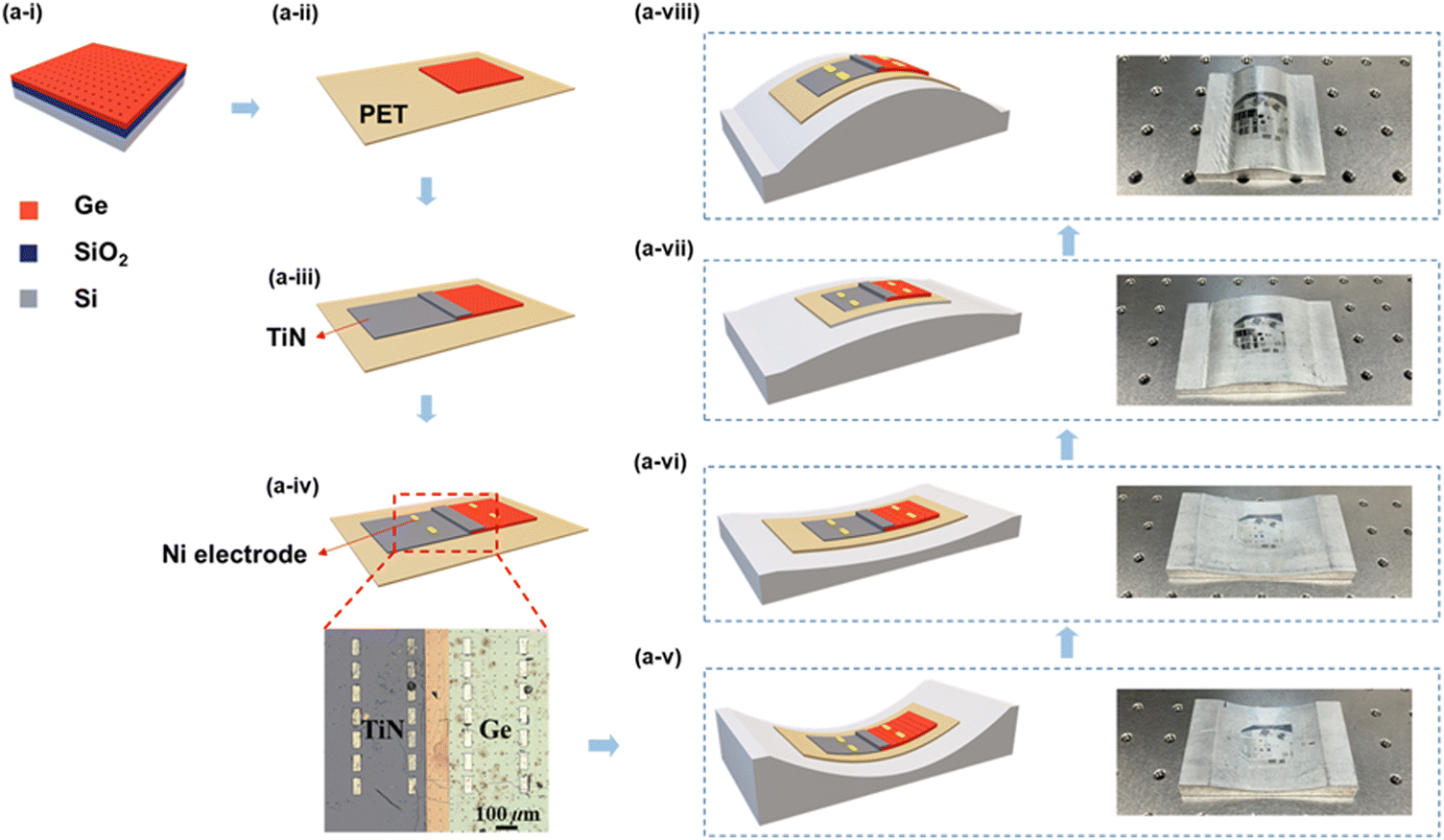 | ||
| Fig. 1 Fabrication process of flexible TiN/Ge PDs and strain modulation by applying external strain. Schematic illustration of (a-i) patterned GeOI by dry etching, (a-ii) Ge NM transferred on PET substrates, followed by (a-iii) TiN deposition, and (a-iv) Ni electrode deposition and the microscopic image of the fabricated TiN/Ge PDs. (a-v–viii) Application of compressive and tensile strain to the devices. | ||
The refractive index and extinction coefficient were characterized using an ellipsometer (J.A. Woollam Spectroscopic Ellipsometer). To further investigate the effect of the TiN layer, optical absorption simulation was carried out using a finite-difference time domain (FDTD) simulator (Lumerical). We used the actual thicknesses of the layers (Ge NM: 300 nm and TiN: 42 nm) and experimentally obtained optical parameters (i.e. refractive index and extinction coefficient).
The resultant devices were characterized using a homemade setup. The setup includes a microscope, a probe platform, a tunable laser (MF12L2-InF3), and a semiconductor parameter analyzer (Keithley 2450). The devices were characterized under various strain values during the measurement by placing them on the convex and concave fixtures.
Results and discussion
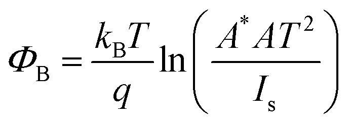
Fig. 2(a) illustrates a schematic image of the TiN/Ge Schottky diode, including the top TiN/Ge Schottky contact and bottom Ge/Au contact. Fig. 2(b) presents a current–voltage (I–V) curve between TiN and Au, confirming the Schottky contact between TiN/Ge with a saturation current of 19 μA as the contact between Ge/Au is ohmic.21,22Fig. 2(c) shows the band diagram of the heterojunction between TiN and Ge. TiN on Ge has an electron work function Φ of 4.3–4.65 eV23 and the electron affinity χ, band gap Eg, and Φ of Ge are found to be 4 eV, 0.69 eV, and 4.17 eV, respectively.13 These figures indicate that a Schottky contact formed between the TiN and Ge. The SBH was calculated from the following equation:where kB = 1.38 × 10⁻²³ m2 kg s−2 K−1 is the Boltzmann constant, T is the Kelvin temperature, q is the electron charge, A* is the Richardson constant, A is the Schottky contact area in cm2, and Is is the reverse saturation current. By solving the equation under room temperature conditions, ΦB turns out to be 0.449 eV, which is similar to previously reported data.24
 | ||
| Fig. 2 (a) Schematic of the TiN/Ge Schottky diode and I–V measurement to extract the SBH between Ge and TiN. (b) I–V curve of the TiN/Ge Schottky diode. The red dashed line shows the saturation current. (c) Band diagram of the TiN/Ge heterojunction. | ||
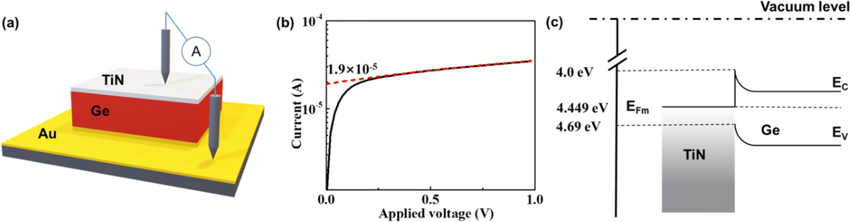
Fig. 3 shows the measured refractive index and extinction coefficient of TiN and Ge, schematic cross-section of the simulated structures, and simulated absorption of Ge and TiN/Ge structures. As shown in Fig. 3(a and b), the refractive index and extinction coefficient of Ge decreased gradually and they decreased substantially around 1.5 μm, while those of TiN increased when the wavelength increased. The refractive index of Ge and TiN intersects at the wavelength of 1606 nm, indicating that TiN has a lower refractive index than Ge below the wavelength of intersection point. This result suggests that more reflections occur at the GeSn surface below TiN, resulting in the enhanced absorption when the wavelength is below the intersection point. Moreover, TiN showed a much higher extinction coefficient from 3.7 to 5.3 compared to Ge (<0.17) when the wavelength increased from 1 to 2 μm. This suggests that TiN deposition on top of GeSn increases the absorption of photons due to reduced reflection at the surface. As shown in Fig. 3(d), TiN/Ge exhibited enhanced absorption in the wavelength range smaller than 1606 nm. This could be ascribed to the lower refractive index of TiN than that of Ge. Light reflection that occurs on the Ge surface can be reduced by top TiN due to its lower refractive index. It is notable that enhanced absorption was also observed in the wavelength range longer than 1606 nm. This could be ascribed to a higher extinction coefficient of TiN throughout the measured wavelength range, suggesting that TiN can act as an excellent photon absorber. Moreover, enhanced absorption can also be ascribed to the LSPR produced by TiN deposited on Ge, allowing more photons to reach the Ge surface. Fig. 3(e) and (f) show the simulated absorption of Ge and TiN/Ge when the wavelength of incident light is 1.5 μm. The intensity of absorption at the interface of air/TiN/Ge is significantly increased compared to the interface of air/Ge due to the resonance of TiN surface plasmon when the NIR light is irradiated. This combined effect allows increased absorption inside TiN/Ge throughout the measured wavelength range.
 | ||
| Fig. 3 Refractive index and extinction coefficient of (a) Ge and (b) TiN in the wavelength range of 1 to 2 μm. (c) Schematic cross-sectional structure of the Ge PD (case 1) and TiN/Ge PD (case 2). (d) Simulated light absorption plots of the TiN/Ge junction and Ge from 1 to 2 μm. Simulated light absorption of cross-sectional maps of (e) Ge and (f) interfaces at TiN/Ge. The wavelength of incident light in the simulation is 1.5 μm. | ||
Fig. 4(a) shows the dark current of Ge and TiN/Ge PDs under flat conditions. The dark current of the TiN/Ge PD is lower than that of the Ge PD in the region of voltage bias from −4 to 4 V. This result is ascribed to the formation of a SBH of 0.449 eV between TiN and Ge, impeding the electrons to flow from TiN to Ge. However, as shown in Fig. 4(b and c), TiN/Ge shows a higher photocurrent and responsivity in the wavelength range of 1200 to 1600 nm with a voltage bias of −1 V. After the heterojunction is made between Ge and TiN, electron hole pairs generated in Ge by incident light are separated efficiently due to the built-in voltage, resulting in enhanced photocurrent and responsivity. The maximum responsivity of the Ge PD was measured to be 16 mA W−1 at 1370 nm. After introducing TiN, the maximum responsivity of TiN/Ge PD was increased to 22 mA W−1 at 1390 nm by 38%. The enhanced peak responsivity could be ascribed to the absorption improvement by the TiN layer. Increased absorption can be achieved by the LSPR effect induced by the TiN layer and reduced reflection as the TiN with a lower refractive index covers the Ge with a higher refractive index.
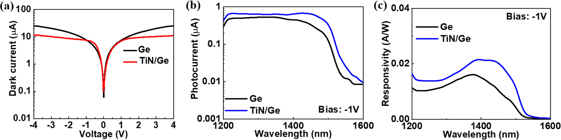 | ||
| Fig. 4 (a) Dark current of Ge and TiN/Ge PD under flat conditions. (b) Photocurrent and (c) responsivity of Ge and TiN/Ge PD under flat conditions with a bias of −1 V. | ||
In the following, we focus on the effect of strain modulation on the responsivity of Ge and TiN/Ge PDs. Fig. 5(a) shows the responsivity of Ge PDs with various strain modulation from −0.25% compressive strain to 0.30% tensile strain. Increasing trend of responsivity can be observed as the tensile strain increases. The increase in responsivity originates from the reduced direct bandgap of Ge due to the uniaxial tensile strain, shifting the absorption edge toward longer wavelength.8 Tensile strain increases the lattice constant, pushing atoms to be further away from each other. As a result, the bandgap decreases due to reduced orbital hybridization.25 Also, tensile strain results in interband transition due to the split of the valence band into light hole (lh) and heavy hole (hh). Under tensile strain conditions, the direct bandgap decreases as the lh band moves upward and at the same time, the Γ-conduction band moves downward. On the other hand, the responsivity decreases as compressive strain increases. Compressive strain decreases the lattice constant, pushing atoms to be closer to each other. This enhances orbital hybridization, resulting in larger splitting of the occupied bands and empty bands. The direct bandgap increases with the increase of compressive strain, and the responsivity reduces correspondingly. Fig. 5(b) shows the responsivity after TiN deposition. It can be clearly seen that the responsivity increases on every strain modulation throughout the wavelength range due to the LSPR caused by the TiN heterojunction. It is worth noting that the wavelength shift toward longer wavelength in peak responsivity is observed after TiN deposition. Such enhancement in responsivity is attributed to the sub-bandgap photon absorption. As a result, as shown in Fig. 5(c), unstrained TiN/Ge PDs exhibit a wavelength shift in peak responsivity from 1363 to 1433 nm and the peak responsivity is increased from 16.7 to 27.3 mA W−1. Moreover, after applying 0.30% of tensile strain on TiN/Ge PDs, the peak responsivity is increased by 98.9% compared to unstrained TiN/Ge PDs, reaching 54.3 mA W−1.
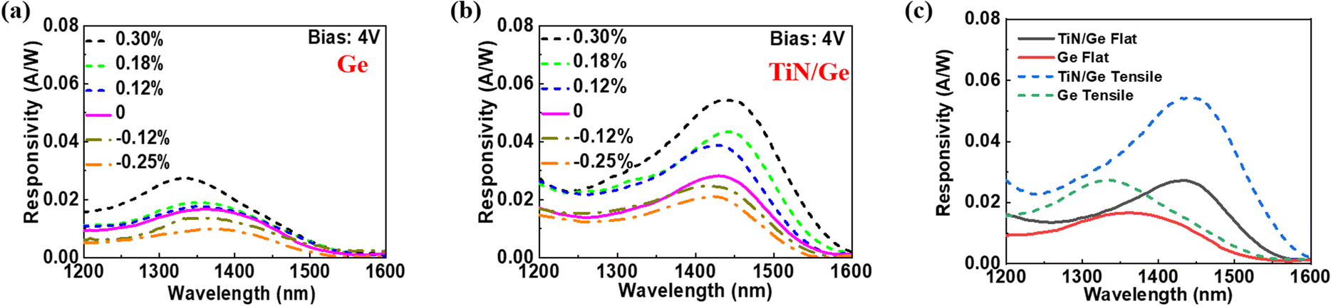 | ||
| Fig. 5 Responsivity of flexible (a) Ge PDs and (b) TiN/Ge PDs under various tensile (short-dashed line) and compressive (dash-dotted line) strain with a bias of 4 V. (c) Comparison of responsivity of flat Ge, Ge with tensile strain, flat TiN/Ge, and TiN/Ge with tensile strain. | ||
Conclusion
In summary, enhanced responsivity of the TiN/Ge PD in the NIR range was achieved by introducing TiN on top of Ge NMs by forming strong local field effects using LSPR and reducing the direct bandgap of Ge by applying tensile strain in the active region. To examine the effect of TiN on light absorption, the refractive index and extinction coefficient of Ge and TiN were measured in the wavelength range of 1000 to 2000 nm. Under light irradiation with a wavelength longer than 1.55 μm, the increase of extinction coefficient in TiN can stimulate the absorption of longer wavelength light, leading to an enhanced NIR absorption of the TiN/Ge PD. To further investigate the effect of strain modulation on responsivity, various compressive strain (−0.25 and −0.12%) and tensile strain (0.12, 0.18, and 0.30%) were applied to the devices. Under compressive strain, the responsivity decreased due to the increased bandgap of Ge compared to that of flat PD. In contrast, under tensile strain, responsivity increased due to the decreased direct bandgap of Ge. The responsivity of the TiN/Ge PD under 0.30% tensile strain was increased 2 times higher compared to that of the flat TiN/Ge PD and 3.3 times higher than that of the flat Ge PD. Therefore, the integration of TiN and Ge provides an excellent platform to achieve flexible NIR PDs with enhanced performance via LSPR and strain modulation.Conflicts of interest
There are no conflicts to declare.Acknowledgements
This work was supported by the A*STAR, Singapore, Advanced Manufacturing and Engineering (AME) Individual Research Grant (IRG) under the Project M21K2c0107, and Ministry of Education, Singapore, under the Grant ACRF Tier 2 grant (MOE-T2EP50120-0001, T2EP50121-0001 (MOE-000180-01)) and AcRF Tier 1 grant (2021-T1-002-031 (RG112/21)). G. E. C. acknowledges the support from Ministry of Science and Technology, Taiwan under Project number MOST 111-2636-E-194-002. The authors also acknowledge the support from the Nanyang NanoFabrication Centre (N2FC).References
- M. Kim, S. Yi, J. D. Kim, X. Yin, J. Li, J. Bong, D. Liu, S.-C. Liu, A. Kvit and W. Zhou, Enhanced performance of Ge photodiodes via monolithic antireflection texturing and α-Ge self-passivation by inverse metal-assisted chemical etching, ACS Nano, 2018, 12(7), 6748–6755 CrossRef CAS PubMed.
- J. Michel, J. Liu and L. C. Kimerling, High-performance Ge-on-Si photodetectors, Nat. Photon., 2010, 4(8), 527–534 CrossRef CAS.
- D. Nam, D. Sukhdeo, A. Roy, K. Balram, S.-L. Cheng, K. C.-Y. Huang, Z. Yuan, M. Brongersma, Y. Nishi and D. Miller, Strained germanium thin film membrane on silicon substrate for optoelectronics, Opt. Express, 2011, 19(27), 25866–25872 CrossRef CAS PubMed.
- M. Kim, S.-C. Liu, T. J. Kim, J. Lee, J.-H. Seo, W. Zhou and Z. Ma, Light absorption enhancement in Ge nanomembrane and its optoelectronic application, Opt. Express, 2016, 24(15), 16894–16903 CrossRef CAS PubMed.
- M. Cho, J.-H. Seo, M. Kim, J. Lee, D. Liu, W. Zhou, Z. Yu and Z. Ma, Resonant cavity germanium photodetector via stacked single-crystalline nanomembranes, J. Vac. Sci. Technol., B: Nanotechnol. Microelectron.: Mater., Process., Meas., Phenom., 2016, 34(4), 040604 Search PubMed.
- J. H. Seo, K. Zhang, M. Kim, D. Zhao, H. Yang, W. Zhou and Z. Ma, Flexible phototransistors based on single-crystalline silicon nanomembranes, Adv. Opt. Mater., 2016, 4(1), 120–125 CrossRef CAS.
- Y. Li, A. Alian, M. Sivan, L. Huang, K. W. Ang, D. Lin, D. Mocuta, N. Collaert and A. V.-Y. Thean, A flexible InGaAs nanomembrane PhotoFET with tunable responsivities in near-and short-wave IR region for lightweight imaging applications, APL Mater., 2019, 7(3), 031503 CrossRef.
- S. An, S. Wu, C. S. Tan, G.-E. Chang, X. Gong and M. Kim, Modulation of light absorption in flexible GeSn metal–semiconductor–metal photodetectors by mechanical bending, J. Mater. Chem. C, 2020, 8(39), 13557–13562 RSC.
- Y.-Y. Zhang, Y.-X. Zheng, J.-Y. Lai, J.-H. Seo, K. H. Lee, C. S. Tan, S. An, S.-H. Shin, B. Son and M. Kim, High Performance Flexible Visible-Blind Ultraviolet Photodetectors with Two-Dimensional Electron Gas Based on Unconventional Release Strategy, ACS Nano, 2021, 15(5), 8386–8396 CrossRef CAS PubMed.
- W. Ouyang, F. Teng, J. H. He and X. Fang, Enhancing the photoelectric performance of photodetectors based on metal oxide semiconductors by charge-carrier engineering, Adv. Funct. Mater., 2019, 29(9), 1807672 CrossRef.
- L. Li, J. Liu and T. Zhu, Study of plasmon resonance, IOP Conf. Ser.: Mater. Sci. Eng., IOP Publishing, 2018, p. 012101 Search PubMed.
- J. Zhang, X. Zhang, J. Li, Z. Ma, B. Leng, Q. Xia, L. Shen, Y. Song, Z. Fu and S. Feng, Simultaneous visible and ultraviolet photoresponse improvement of MoS2/ZnO heterostructure photodetector via direct resonant coupling of Au nanoparticles localized surface plasmon resonance, Opt. Mater., 2022, 124, 111997 CrossRef CAS.
- S. L. Shinde, S. Ishii and T. Nagao, Sub-band gap photodetection from the titanium nitride/germanium heterostructure, ACS Appl. Mater. Interfaces, 2019, 11(24), 21965–21972 CrossRef CAS PubMed.
- B. Doiron, M. Mota, M. P. Wells, R. Bower, A. Mihai, Y. Li, L. F. Cohen, N. M. Alford, P. K. Petrov and R. F. Oulton, Quantifying figures of merit for localized surface plasmon resonance applications: a materials survey, ACS Photonics, 2019, 6(2), 240–259 CrossRef CAS.
- B. Doiron, Y. Li, A. Mihai, R. Bower, N. M. Alford, P. K. Petrov, S. A. Maier and R. F. Oulton, Plasmon-enhanced electron harvesting in robust titanium nitride nanostructures, J. Phys. Chem. C, 2019, 123(30), 18521–18527 CrossRef CAS.
- S. Podder, J. Bora, S. Thakur, D. Gogoi, B. Basumatary, S. M. Borah, N. C. Adhikary and A. R. Pal, Interband transition in plasmonic titanium nitride and its contribution towards ZnO based pyro-phototronic application, Mater. Chem. Phys., 2022, 275, 125290 CrossRef CAS.
- U. Guler, V. M. Shalaev and A. Boltasseva, Nanoparticle plasmonics: going practical with transition metal nitrides, Mater. Today, 2015, 18(4), 227–237 CrossRef CAS.
- S. Podder and A. R. Pal, Plasmonic visible-NIR photodetector based on hot electrons extracted from nanostructured titanium nitride, J. Appl. Phys., 2019, 126(8), 083108 CrossRef.
- N. A. Gusken, A. Lauri, Y. Li, T. Matsui, B. Doiron, R. Bower, A. Regoutz, A. Mihai, P. K. Petrov and R. F. Oulton, TiO2–x-enhanced IR hot carrier based photodetection in metal thin film–Si junctions, ACS Photonics, 2019, 6(4), 953–960 CrossRef CAS.
- S. An, Y. Liao and M. Kim, Flexible Titanium Nitride/Germanium-Tin Photodetectors Based on Sub-Bandgap Absorption, ACS Appl. Mater. Interfaces, 2021, 13(51), 61396–61403 CrossRef CAS PubMed.
- Z. Xia, H. Song, M. Kim, M. Zhou, T.-H. Chang, D. Liu, X. Yin, K. Xiong, H. Mi and X. Wang, Single-crystalline germanium nanomembrane photodetectors on foreign nanocavities, Sci. Adv., 2017, 3(7), e1602783 CrossRef PubMed.
- C.-J. Kim, H.-S. Lee, Y.-J. Cho, K. Kang and M.-H. Jo, Diameter-dependent internal gain in ohmic Ge nanowire photodetectors, Nano Lett., 2010, 10(6), 2043–2048 CrossRef CAS PubMed.
- S. A. Vitale, J. Kedzierski, P. Healey, P. W. Wyatt and C. L. Keast, Work-function-tuned TiN metal gate FDSOI transistors for subthreshold operation, IEEE Trans. Electron Devices, 2010, 58(2), 419–426 Search PubMed.
- H. Wu, W. Huang, W. Lu, R. Tang, C. Li, H. Lai, S. Chen and C. Xue, Ohmic contact to n-type Ge with compositional Ti nitride, Appl. Surf. Sci., 2013, 284, 877–880 CrossRef CAS.
- J. Qi, X. Qian, L. Qi, J. Feng, D. Shi and J. Li, Strain-engineering of band gaps in piezoelectric boron nitride nanoribbons, Nano Lett., 2012, 12(3), 1224–1228 CrossRef CAS PubMed.
Footnotes |
| † Electronic supplementary information (ESI) available. See DOI: https://doi.org/10.1039/d3tc00228d |
| ‡ These authors contributed equally to this work. |
| This journal is © The Royal Society of Chemistry 2023 |