
On the factors affecting the response time of synaptic ion-gated transistors†
Ramin
Karimi Azari
 *,
Tian
Lan
and
Clara
Santato
*
*,
Tian
Lan
and
Clara
Santato
*
Engineering Physics, Polytechnique Montreal, 2500 Ch. Polytechnique, H3T 1J4, Montreal, QC, Canada
First published on 11th May 2023
Abstract
Ion-Gated Transistors (IGTs) feature the processing rate of the human brain for neuromorphic computing. Furthermore, they require low power for training and deployment of neural network algorithms. Neuromorphic computing requires both long-term and short-term potentiation, within the same device. The nature of the doping mechanism in IGTs affects their time-resolved properties, key for their use as neuromorphic devices. Depending on the permeability of the semiconducting channel to ions, IGTs undergo electrochemical (three-dimensional) or electrostatic (field-effect, two-dimensional) doping, which leads to a wide range of IGT response times. Here, we propose a methodology to control the response time of IGTs made up of films of poly(3-hexylthiophene (P3HT) as the semiconducting channel and the ionic liquid 1-ethyl-3-methylimidazolium bis(trifluoromethanesulfonyl)imide [EMIM][TFSI] as the gating medium. The methodology includes the effect of the pulse frequency of the applied gate-source voltage (Vgs), the number of applied Vgs pulses, and the Vgs pulse duration. It also considers the effect of the values of the applied Vgs and drain-source (Vds) voltages. Last but not least, the methodology includes the effect of the Vgs sampling time. Our results contribute to the understanding of how to achieve plasticity in IGTs.
10th Anniversary StatementIn a battery, we find both electronic and ionic conduction. These two types of conduction also coexist in ion-gated transistors (IGTs), making use of ionic gating media (e.g. saline aqueous solutions and ionic liquids). IGTs are relevant for flexible and printable electronics, and bioelectronics. Furthermore, a three-terminal IGT closely resembles the biological synapse since the gate electrode acts as a neuron that applies the presynaptic spike and generates a postsynaptic current spike in the semiconducting channel, acting as a postsynaptic neuron. In this work, we propose a methodology that achieves synaptic plasticity in IGTs. We demonstrate that IGTs can be employed as neuromorphic devices integrating memory (long-term plasticity) and processing functions (short-term plasticity) in the same device, as a function of the electrical biasing conditions. We think that by reaching the convergence of electronic materials, ionic materials, low power electronics, device engineering, and neurosciences, our work can help to celebrate the 10th anniversary issue of the Journal of Materials Chemistry C. |
Introduction
Ion-Gated Transistors (IGTs) make use of ionic compounds as the gating media. IGTs play a crucial role in the development of neuromorphic computing devices, due to their low operating voltages (sub-1 V), viable functionalization of the semiconducting channel for chemo and biosensing purposes, and possible fabrication into large device arrays.1,2 Due to their combined electronic and ionic transport,3–5 IGTs are relevant for future computation, bioelectronics, and electrochemical energy storage.6–11Since the electrical double layer (EDL) at the interface between the semiconducting transistor channel and the ion gating medium is thin (3–4 nm), the specific capacitance observed in IGTs can be as high as 10 μF cm−2, resulting in a large density of charge carriers (about 3 × 1015 cm−2), at low Vgs biases.12–14
Several working mechanisms are possible for IGTs based on organic semiconducting channel materials, depending on the degree of permeability of the channel to ions. Ion-impermeable channels are electrostatically doped (as in conventional field-effect transistors, where the doping is bidimensional) whereas ion-permeable channels can be electrochemically doped (in this case the doping is three-dimensional).15
Certainly, IGTs can feature a combination of these two working mechanisms, where the weight of each contribution depends on the specific semiconductor and gating medium, the quality of their interface, and the electrical biasing conditions. For instance, in organic single crystal channels poorly permeable to ions, upon application of a gate-source voltage (Vgs), ions accumulate at the ionic medium–organic semiconductor interface, bringing about electrostatic doping.14,16–19
The nature of the ionic medium (e.g., solid, gel, or liquid) influences the movement of the ions in the gating media of IGTs, in turn affecting the transistor performance and response time.10,20–24
Room-temperature ionic liquids (ILs) are ideal gating media for IGTs since they feature a high conductivity (0.1–20 mS cm−1), a wide range of viscosity (10–1000 mPa s), and minimal volatility.25,26 Furthermore, their electrochemical stability window can be as high as 5 V.16,27,28
We can establish a correspondence between the working principle of IGTs and fundamental processes taking place in the brain (Fig. 1a). In the human brain, a neuronal network of around 1011 neurons is linked by approximately 1015 synapses. Synapses are a passageway for conveying action potentials from presynaptic to postsynaptic neurons. They carry out parallel information computing (processing and memorizing information) by adjusting the synaptic weight, i.e. the strength of a synaptic connection29 (with the term synaptic strength referring to the amount of current generated in the postsynaptic neuron as a result of an action potential in the presynaptic neurons).
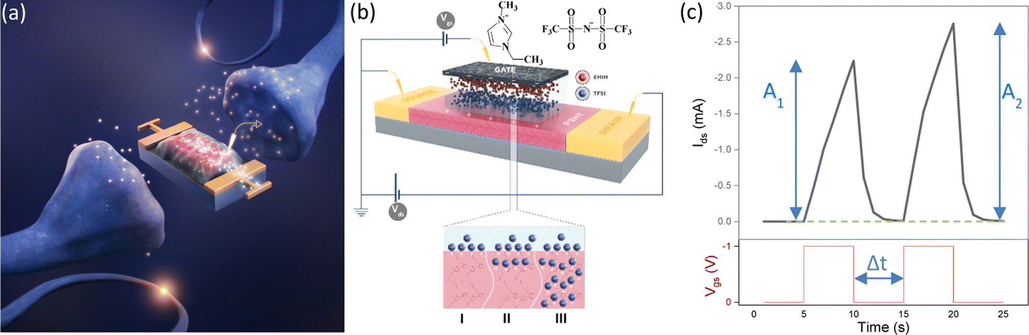 | ||
| Fig. 1 (a) Bio-inspired synaptic IGT transistor. (b) Device scheme and possible doping regimes (I to III) upon application of a negative Vgs to a P3HT-based IGT; molecular structures of the ions constituting the ionic liquid employed as gating medium in this study. (c) A pair of successive Vgs inputs (−1 V) for 5 s with a pulse interval Δt = 5 s applied to an IGT. A1 and A2 are the amplitudes of the drain–source current (Ids). | ||
The rate of enhancement in the current amplitude after the second of two repetitive excitatory postsynaptic potentials (EPSPs) with an interval Δt is an index of the increase of the synaptic strength in a synaptic transistor, measured as paired pulse facilitation (PPF), defined as (A2−A1)/A1 × 100 (Fig. 1c).30
The three-terminal IGT closely resembles the biological synapse (Fig. 1a and b) since the gate electrode acts as a neuron that applies the presynaptic spike (Vgs) and generates a postsynaptic current (PSC) spike in the semiconducting channel (acting as a postsynaptic neuron) between source and drain electrodes (drain–source current, Ids).
In an IGT artificial synapse, the synaptic plasticity can be described as the alteration of the synaptic weight and the IGT channel conductivity.9 The synaptic weight is modulated independently via the gate terminal, in an IGT.31 Short-term plasticity (STP) and long-term plasticity (LTP) are two categories of synaptic plasticity. A persistent modification of synaptic weight, LTP, supports memory and learning and lasts longer than a transient modification, STP. STP is necessary for data processing, encoding and filtering.32,33
An important aspect of synaptic plasticity modulation in IGTs is its response time, e.g., the time it takes for the PSC of a transistor to reach a steady state after removal of the Vgs bias.
Response time can vary depending on the specific device structure, materials, and operating conditions.
We can consider two contributions to the Ids decay in IGTs. The former is a fast current decay due to the removal of electrical double layers and/or ions located within a thin depth in the channel. The latter is a slow current decay related to the removal of the ions located deep in the channel and/or trapped.10,24,34,35
According to Bernards,10 in IGTs, the response time of Ids with respect to a change in Vgs can be fit by exponential functions. Ids(t) for the case of a square Vgs step follows a time dependence given by
 | (1) |
The majority of organic synaptic devices can only partially mimic synaptic plasticity, either LTP or STP, depending on the doping mechanism. One of the most significant challenges in IGTs is to transition plasticity from STP to LTP and vice versa in a single device and control the response time for various applications.36–38 To tackle this challenge, aspects pertaining to the chemical nature and structure of the channel material and ionic medium, device structure and electrical bias input stimuli, should be all considered.29
In this study, we control the synaptic plasticity and response time of IGTs by controlling input Vgs and Vds stimuli to modulate STP and LTP. We employed poly(3-hexylthiophene) (P3HT) as the organic transistor channel material, gated with the ionic liquid (1-ethyl-3-methylimidazolium bis(trifluoromethanesulfonyl)imide) ([EMIM][TFSI]) (Fig. 1b). We studied various aspects of bio-inspired synaptic transmission in [EMIM][TFSI]-gated P3HT transistors, such as spike frequency-dependent plasticity (SFDP) (defined as (A5−A1)/A1 × 100 for different frequencies of Vgs for a train of five pulses) and spike number-dependent plasticity (SNDP) (defined as (An − A1)/A1 × 100% where n > 1 is the number of Vgs pulse). Furthermore, we investigated the influence of the sampling time of applied Vgs on the measured response time.
Results and discussion
Film morphology
AFM images show that the spin-coated P3TH films are continuous, with a root mean square (rms) roughness of ca. 3.77 ± 1.04 nm in a 10 μm × 10 μm-sized area (Fig S1a–c, ESI†). The XRD patterns of the P3HT films show a peak related to the lamellar structure located at 2θ = 5.1° (Fig. S1d, ESI†).39Transfer and output characteristics of [EMIM][TFSI]-gated P3HT transistors
The IGT transfer and output characteristics show a typical p-type behavior of transistors working in accumulation mode. We observed that the hysteresis decreases with the Vgs scan rate from 100 to 5 mV s−1 due to the increased time available to accommodate ion movement (Fig. 2a and Fig. S2a–c, ESI†). We deduced a threshold voltage of ca. −0.4 V, ON/OFF of ca. 102, mobility of 0.1 cm2 V−1 s−1, and charge carrier density of 3.0 × 1015 cm−2, at 100 mV s−1 (values obtained at 50, 25, and 5 mV s−1 are reported in Table S1, ESI†).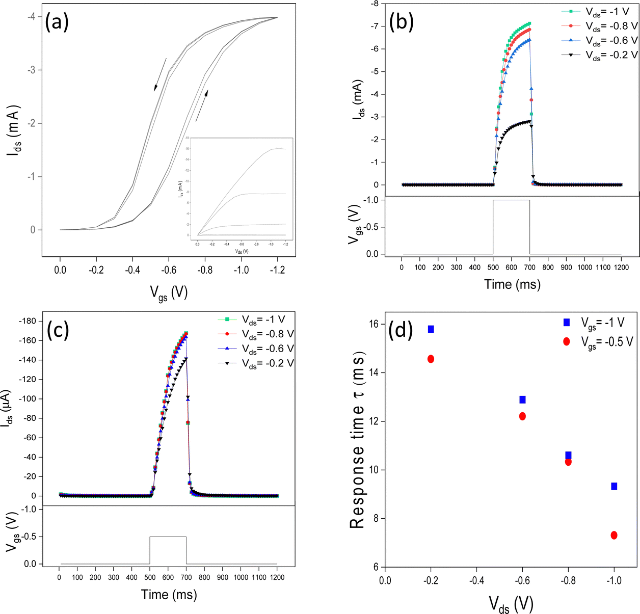 | ||
| Fig. 2 Characteristics of [EMIM][TFSI]-gated P3HT transistors. (a) Transfer characteristics in the linear regime (Vds = −0.2 V, (3 cycles)) at Vgs 100 mV s−1 scan rate (inset: output characteristic with Vgs = 0, −0.2, −0.4, −0.6, −0.8, −1 V and Vds 100 mV s−1 scan rate). Ids response to (b) Vgs = −1 V, (c) Vgs = −0.5 V, at different Vds. The duration time of the Vgs bias is 200 ms. (d) Transient response of an [EMIM][TFSI]-gated P3HT transistor versus Vds in different values of Vgs square step. | ||
Influence of the value of Vgs on the response time
We performed a typical Ids transient response characterization (Fig. 2b and c) using a 200 ms-long square Vgs pulse with amplitudes −0.5 and −1 V, at Vds = −0.2, −0.6, −0.8, and −1 V. Low amplitude Vgs (pre-synaptic spike) pulses are expected to induce the formation of electrical double layers and dope regions in P3HT close to the interface and/or amorphous. These regions can rapidly de-dope and PSC rapidly decays; this response is analogous to STP. We observed that the response time increased with the increase of Vgs. For instance, increasing Vgs from −0.5 V to −1 V (Vds = −1 V) increases the response time from 7.31 to 9.33 ms, i.e. by 27%. Higher values of Vgs induce a deeper anion penetration in the film, possibly including crystalline regions. This implies longer times for ion removal prior reaching the steady state, after the removal of Vgs (Fig. 2d).Influence of the value of Vds on the response time
We observed that the response time halves in a quasi-linear trend, in the region of Vgs included between −0.5 V and −1 V (Fig. 2d). According to Bernards’ model (eqn (1)), the ratio τe/τi is determined by τe/τi ∼ dL2/ μVds−1 where d is the ionic gating medium thickness, L is the channel length and other symbols have been already introduced. In agreement with the model, the increase of Vds is expected to cause the decrease in the response time; this is actually what we observed.Effect of the number of Vgs pulses on the response time
To explore the synaptic properties of [EMIM][TFSI]-gated P3HT transistors, we applied an increasing number of Vgs pulses (5, 10, and 25). As the number of pulses increased, so did the response time. Upon application of a Vgs pulse, ions move towards/into the channel materials (Fig. 3). With increasing the number of pulses, the time needed for the anions to redistribute in the p-type P3HT increases, since they penetrate deeper into the film, which can include ion traps. This result can be exploited to drive the device transition from STP to LTP. In other words, the repetition of the stimuli leads to a learning process, in our synaptic IGTs.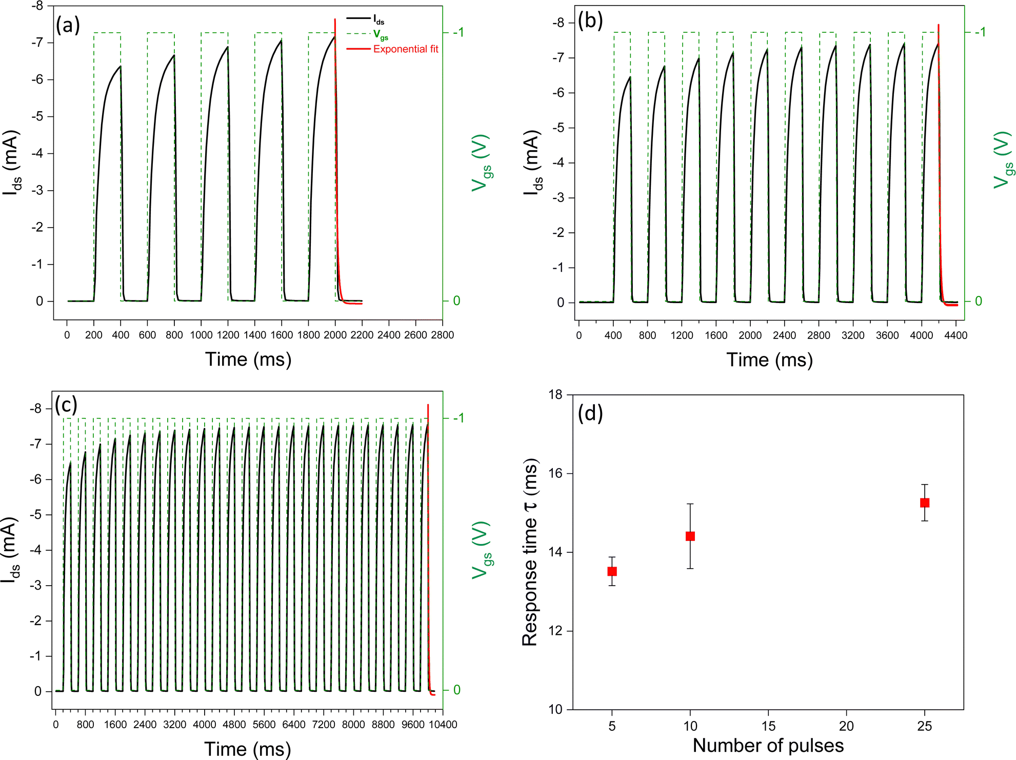 | ||
| Fig. 3 Transient Ids response of [EMIM][TFSI]-gated P3HT transistors in response to different numbers of Vgs square step train pulses. Vgs = −1 V at Vds = −0.6 V (a) 5 pulses, (b) 10 pulses, (c) 25 pulses. (d) Response time versus number of Vgs pulses. The duration and interval of each Vgs pulse is 200 ms; exponential fits used to estimate the response time are in red. | ||
We observed that SNDP1–5 (where SNDP1–n = (An−A1)/A1 × 100) is 13%, SNDP1–10 is 15%, and SNDP1–25 is 17%. These values quantitatively describe the evolution of the SNDP index for our synaptic IGTs.
Impact of the pulse duration time on response time
Increasing the pulse duration time brings about more time for the ions to penetrate the channel. This leads to an increase in the de-doping time and, in turn, an increase in the response time upon removal of the Vgs bias. According to Fig. 4a and b, increasing the pre-synaptic spike pulse duration time from 10 ms to 9 s, at Vgs = −1 V, induces an increase of the amplitude of the excitatory postsynaptic drain–source current (EPSC), suggesting a more important synaptic weight change. Literature on IL-gated P3HT transistors reports response times depending on the specific device structure and operating conditions.29,40,41 Frisbie et al., observed a response time of about 1 ms for ion-gel-gated P3HT transistors with Vgs = −3 V and pulse duration of 0.5 ms.29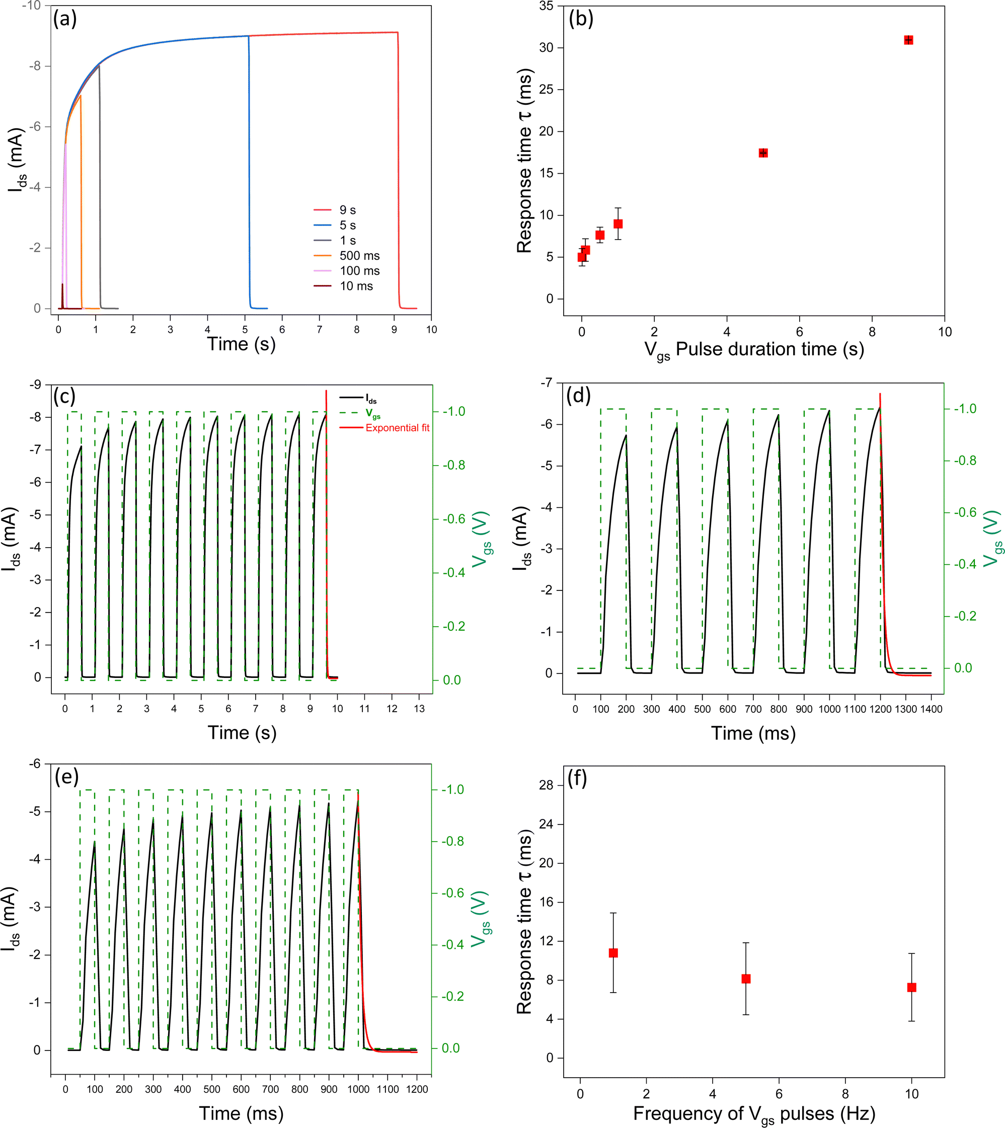 | ||
| Fig. 4 (a) and (b) Transient Ids characteristic response of an [EMIM][TFSI]-gated P3HT transistor versus different duration times. Transient response of transistors in response to Vgs pulses with different frequencies (c) 1 Hz, (d) 5 Hz, and (e) 10 Hz. (f) Response time versus frequency of Vgs pulses (Vgs = −1 V, at Vds = −0.6 V). | ||
Impact of the frequency of the Vgs pulses on the response time
Given the inverse relationship between frequency and pulse duration time, response time is expected to decrease as the frequency of the Vgs increases (Fig. 4c–f). This observation is explained by considering that the decrease in the duration time of the Vgs pulses brings about a shorter time for ion penetration in the channel (and therefore a shorter depth of penetration of the ions in the P3HT film). This finding is reminiscent of the spike frequency-dependent plasticity (SFDP) of the biological synapses. The SFDP index after six consecutive spikes at frequencies included between 1 Hz and 25 Hz increased from 12% to 15%.Importance of the Vgs sampling time on the measurement of the response time
We investigated the impact of the sampling time of square Vgs pulses (with a constant duration time) on the response time. The sampling time is the time difference between two Vgs readings taken at two consecutive instants, during the measurement; it permits converting a continuous-time signal into a discrete-time one. By decreasing the sampling time during transient responses, it is possible to obtain more accurate Ids measurements and, in turn, more accurate evaluation of the time response (Fig. 5 and Fig. S3, ESI†).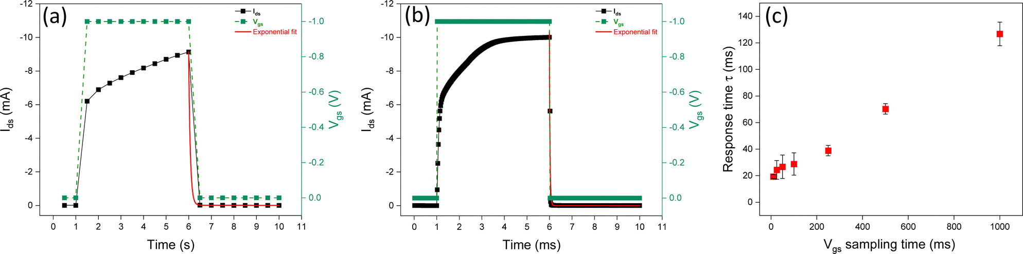 | ||
| Fig. 5 Transient response of an [EMIM][TFSI]-gated P3HT transistor at different Vgs pulse sampling times: (a) 500 ms, (b) 25 ms; the duration of Vgs pulse is 5 s. (c) Response time versus different Vgs sampling times (10, 25, 50, 100, 200, 500, and 1000 ms) at Vds = −0.8 V. | ||
Experimental
Films of P3HT with regioregular intermediatemolecular weight (50–70 kDa, RIEKE metals), deposited on bare SiO2/Si substrates, were employed as channel materials of our [EMIM][TFSI]-gated IGTsSiO2/Si substrates were photolithographically patterned with source and drain electrodes (40 nm-thick Au on a 5 nm-thick Ti adhesion layer) with interelectrode distance, L, of 10 μm and width, W, of 4 mm. Prior to the deposition of the P3HT films, the substrates were cleaned in sequential steps of 10 min in isopropyl alcohol, 10 min in acetone and 10 min in isopropyl mg P3HT in 1 ml chlorobenzene and stirred overnight in a N2 glove box (<5 ppm O2, H2O).P3HT films were deposited by spin-coating on the pre-patterned SiO2/Si substrate and placed on a hot plate at 140 °C for 2 hours in the N2 glove box. [EMIM][TFSI] (IoLiTec, >99%)) was purified under vacuum conditions (ca 10−5 torr) for 24 hours at 60 °C before use. The ionic liquid was dropped on a DuraporeR membrane (typically 4 mm × 9 mm-sized and 125 μm-thick) located on the transistor channel. The gate electrode was a high surface area of carbon paper (Spectracarb 2050), 6 mm × 3 mm-sized, 170 μm-thick, coated with an ink made of activated carbon (PICACTIF SUPERCAP BP10, Pica, 28 mg ml−1) and polyvinylidene fluoride (PVDF, KYNAR HSV900, 1.4 mg ml−1) binder in N-methyl pyrrolidone (NMP, Fluka).
Characterization of the films
Atomic Force Microscopy (AFM) images were taken in the air, at room temperature, on a Digital Instruments Dimension 3100, in tapping mode, with Al-coated silicon cantilevers. X-ray diffraction (XRD) spectra of the P3HT films were taken using a Bruker D8 diffractometer with a wavelength (CuKα) of 1.54 Å. 1100 nm).Electrical characterization of the devices
Transistor characteristics were obtained using an Agilent B1500A semiconductor parameter analyzer connected to a house-made micromanipulated electrical probe station located in the N2 glove box.Conclusions
We studied P3HT-based Ion-Gated Transistors (IGTs) as bio-inspired synapses for applications in neuromorphic systems. We investigated the response time and synaptic plasticity of P3HT IGTs by engineering input stimuli such as values of Vgs and Vds, number of pulses of Vgs, Vgs pulse duration time and frequency.Response time and plasticity increased with the value of the applied Vgs and Vgs pulse duration. We were also able to emulate synaptic functions such as short-term plasticity (STP) and long-term plasticity (LTP), and the transition between the two.
We achieved an increased response time via repeated Vgs presynaptic stimuli (spike number-dependent plasticity (SNDP)) and by decreasing pulse frequency (spike frequency-dependent plasticity (SFDP)), all at low driving voltages (about 1 V).
The relevance of our study is that we demonstrate that IGTs can be employed as neuromorphic devices integrating memory (LTP) and processing functions (STP) in the same device, as a function of the electrical biasing conditions.
Work is in progress to address the effect of the structure of the transistor channel material on the correlation between applied bias conditions and response time, by extending our study to films of P3HT at different molecular weights, other organic semiconductors, and printable metal oxides.
Author contributions
R. K. A. and C. S. designed the experiments. R. K. A. and T. L. performed the experiments. R. K. A. and C. S. wrote the manuscript. All authors commented on the manuscript.Conflicts of interest
No conflicts to declare.Acknowledgements
C. S. acknowledges NSERC (Discovery Grant) for financial support.References
- M. Voelker and P. Fromherz, Small, 2005, 1, 206–210 CrossRef CAS PubMed.
- J. J. Jun, N. A. Steinmetz, J. H. Siegle, D. J. Denman, M. Bauza, B. Barbarits, A. K. Lee, C. A. Anastassiou, A. Andrei, Ç. Aydın, M. Barbic, T. J. Blanche, V. Bonin, J. Couto, B. Dutta, S. L. Gratiy, D. A. Gutnisky, M. Häusser, B. Karsh, P. Ledochowitsch, C. M. Lopez, C. Mitelut, S. Musa, M. Okun, M. Pachitariu, J. Putzeys, P. D. Rich, C. Rossant, W. L. Sun, K. Svoboda, M. Carandini, K. D. Harris, C. Koch, J. O'Keefe and T. D. Harris, Nature, 2017, 551, 232–236 CrossRef CAS PubMed.
- C. G. Bischak, L. Q. Flagg, K. Yan, T. Rehman, D. W. Davies, R. J. Quezada, J. W. Onorato, C. K. Luscombe, Y. Diao and C.-Z. Li, arXiv, 2019, preprint, arXiv:1910.06440 DOI:10.48550/arXiv.1910.06440.
- M. Berggren and A. Richter-Dahlfors, Adv. Mater., 2007, 19, 3201–3213 CrossRef CAS.
- J. Rivnay, R. M. Owens and G. G. Malliaras, Chem. Mater., 2014, 26, 679–685 CrossRef CAS.
- D. Moia, A. Giovannitti, A. A. Szumska, I. P. Maria, E. Rezasoltani, M. Sachs, M. Schnurr, P. R. Barnes, I. McCulloch and J. Nelson, Energy Environ. Sci., 2019, 12, 1349–1357 RSC.
- I. E. Jacobs and A. J. Moulé, Adv. Mater., 2017, 29, 1703063 CrossRef PubMed.
- H. Yuan, H. Shimotani, A. Tsukazaki, A. Ohtomo, M. Kawasaki and Y. Iwasa, Adv. Funct. Mater., 2009, 19, 1046–1053 CrossRef CAS.
- L. F. Abbott and S. B. Nelson, Nat. Neurosci., 2000, 3, 1178–1183 CrossRef CAS PubMed.
- D. A. Bernards and G. G. Malliaras, Adv. Funct. Mater., 2007, 17, 3538–3544 CrossRef CAS.
- X. Bu, H. Xu, D. Shang, Y. Li, H. Lv and Q. Liu, Adv. Intell. Syst., 2020, 2, 2000156 CrossRef.
- D. Wang, V. Noël and B. Piro, Electronics, 2016, 5, 9 CrossRef.
- K. Ueno, S. Nakamura, H. Shimotani, A. Ohtomo, N. Kimura, T. Nojima, H. Aoki, Y. Iwasa and M. Kawasaki, Nat. Mater., 2008, 7, 855–858 CrossRef CAS PubMed.
- J. Rivnay, S. Inal, A. Salleo, R. M. Owens, M. Berggren and G. G. Malliaras, Nat. Rev. Mater., 2018, 3, 17086 CrossRef CAS.
- M. J. Panzer and C. D. Frisbie, Adv. Mater., 2008, 20, 3177–3180 CrossRef CAS.
- P. Hapiot and C. Lagrost, Chem. Rev., 2008, 108, 2238–2264 CrossRef CAS PubMed.
- A. Laiho, L. Herlogsson, R. Forchheimer, X. Crispin and M. Berggren, Proc. Natl. Acad. Sci. U. S. A., 2011, 108, 15069–15073 CrossRef CAS PubMed.
- M. Zakrewsky, K. S. Lovejoy, T. L. Kern, T. E. Miller, V. Le, A. Nagy, A. M. Goumas, R. S. Iyer, R. E. Del Sesto and A. T. Koppisch, Proc. Natl. Acad. Sci. U. S. A., 2014, 111, 13313–13318 CrossRef CAS PubMed.
- T.-H. Le, Y. Kim and H. Yoon, Polymers, 2017, 9, 150 CrossRef PubMed.
- H. Shimotani, H. Asanuma, J. Takeya and Y. Iwasa, Appl. Phys. Lett., 2006, 89, 203501 CrossRef.
- R. Giridharagopal, L. Flagg, J. Harrison, M. Ziffer, J. Onorato, C. Luscombe and D. Ginger, Nat. Mater., 2017, 16, 737–742 CrossRef CAS PubMed.
- Y. Xia, J. H. Cho, J. Lee, P. P. Ruden and C. D. Frisbie, Adv. Mater., 2009, 21, 2174–2179 CrossRef CAS.
- J. O. Guardado and A. Salleo, Adv. Funct. Mater., 2017, 27, 1701791 CrossRef.
- E. M. Thomas, M. A. Brady, H. Nakayama, B. C. Popere, R. A. Segalman and M. L. Chabinyc, Adv. Funct. Mater., 2018, 28, 1803687 CrossRef.
- V. Kaphle, S. Liu, A. Al-Shadeedi, C. M. Keum and B. Lüssem, Adv. Mater., 2016, 28, 8766–8770 CrossRef CAS PubMed.
- K. Izutsu, Electrochemistry in nonaqueous solutions, John Wiley & Sons, 2009 Search PubMed.
- L. Kergoat, L. Herlogsson, D. Braga, B. Piro, M. C. Pham, X. Crispin, M. Berggren and G. Horowitz, Adv. Mater., 2010, 22, 2565–2569 CrossRef CAS PubMed.
- M. J. Earle, J. M. Esperança, M. A. Gilea, J. N. Canongia Lopes, L. P. Rebelo, J. W. Magee, K. R. Seddon and J. A. Widegren, Nature, 2006, 439, 831–834 CrossRef CAS PubMed.
- J. H. Cho, J. Lee, Y. He, B. S. Kim, T. P. Lodge and C. D. Frisbie, Adv. Mater., 2008, 20, 686–690 CrossRef CAS.
- S. L. Jackman and W. G. Regehr, Neuron, 2017, 94, 447–464 CrossRef CAS PubMed.
- X. Bu, H. Xu, D. Shang, Y. Li, H. Lv and Q. Liu, Adv. Intell. Syst., 2020, 2, 2000156 CrossRef.
- L. F. Abbott and W. G. Regehr, Nature, 2004, 431, 796–803 CrossRef CAS PubMed.
- M. A. Lynch, Physiol. Rev., 2004, 84, 87–136 CrossRef CAS PubMed.
- E. M. Thomas, B. C. Popere, H. Fang, M. L. Chabinyc and R. A. Segalman, Chem. Mater., 2018, 30, 2965–2972 CrossRef CAS.
- B. C. Popere, G. E. Sanoja, E. M. Thomas, N. S. Schauser, S. D. Jones, J. M. Bartels, M. E. Helgeson, M. L. Chabinyc and R. A. Segalman, J. Mater. Chem. C, 2018, 6, 8762–8769 RSC.
- L.-a Kong, J. Sun, C. Qian, Y. Fu, J. Wang, J. Yang and Y. Gao, Org. Electron., 2017, 47, 126–132 CrossRef CAS.
- C. Qian, L.-a Kong, J. Yang, Y. Gao and J. Sun, Appl. Phys. Lett., 2017, 110, 083302 CrossRef.
- P. Gkoupidenis, N. Schaefer, B. Garlan and G. G. Malliaras, Adv. Mater., 2015, 27, 7176–7180 CrossRef CAS PubMed.
- C. Qian, J. Sun, L. Zhang, H. Huang, J. Yang and Y. Gao, J. Phys. Chem. C, 2015, 119, 14965–14971 CrossRef CAS.
- D. Rawlings, E. M. Thomas, R. A. Segalman and M. L. Chabinyc, Chem. Mater., 2019, 31, 8820–8829 CrossRef CAS.
- G. D. Spyropoulos, J. N. Gelinas and D. Khodagholy, Sci. Adv., 2019, 5, eaau7378 CrossRef CAS PubMed.
Footnote |
| † Electronic supplementary information (ESI) available. See DOI: https://doi.org/10.1039/d3tc00161j |
| This journal is © The Royal Society of Chemistry 2023 |