
Band-engineered dual-band visible and short-wave infrared photodetector with metal chalcogenide colloidal quantum dots†
Pengfei
Zhao‡
a,
Tianling
Qin‡
a,
Ge
Mu
*a,
Shuo
Zhang
a,
Yuning
Luo
 a,
Menglu
Chen
*abc and
Xin
Tang
*abc
a,
Menglu
Chen
*abc and
Xin
Tang
*abc
aSchool of Optics and Photonics, Beijing Institute of Technology, Beijing, China. E-mail: xintang@bit.edu.cn; 7520210145@bit.edu.cn; Menglu@bit.edu.cn
bBeijing Key Laboratory for Precision Optoelectronic Measurement Instrument and Technology, Beijing, China
cYangtze Delta Region Academy of Beijing Institute of Technology, Jiaxing, China
First published on 2nd February 2023
Abstract
Dual-band photodetectors have attracted significant attention because of their potential in optical communication, biochemical detection, and environmental monitoring. Colloidal quantum dots (CQDs) are promising materials for dual-band photodetectors because of their size-tunable bandgaps with wide spectral tunability and easy solution processability. Here, we propose a dual-band visible (VIS) and short-wave infrared (SWIR) detector based on metal chalcogenide CQDs (HgTe and CdTe CQDs). An n-type ZnO layer between the CdTe and HgTe layers is introduced as a hole-blocking layer to prevent hole injection from the different sensing layers, enabling the detector to switch between the VIS and SWIR modes by changing the polarity and magnitude of the bias voltage. The device exhibits an excellent performance with high responsivities of 0.5 and 1.1 A W−1 for the two bands that peak at 700 and 2100 nm, respectively. The detectivity of the device can reach 1.1 × 10¹¹ Jones at +3 V (VIS) and 4.5 × 10¹¹ Jones at −2 V (SWIR). In addition, VIS/SWIR dual-band imaging is realized, which provides more comprehensive object information than single-band detectors.
 Xin Tang | Dr. Xin Tang received his PhD degree from the City University of Hong Kong in 2017 supervised by Dr King W.C. Lai. After graduation, he became a postdoctoral researcher in the James Franck Institute, University of Chicago, in the research group of Prof. Philippe Guyot-Sionnest where he spent a wonderful three years. In 2020, he became a professor at the School of Optics and Photonics, Beijing Institute of Technology. His research interests include multispectral/hyperspectral infrared detectors, colloidal quantum-dot focal plane array imagers, and functional photonic nanostructures. |
Introduction
Visible imaging can offer clear and intuitive details of objects and is consistent with the human visual system.1–3 However, the narrow spectral range in visible light limits the comprehensive acquisition of object information. Beyond the visible band, infrared can provide important optical information on, for example, the molecular composition and thermal distribution.4 Dual-band visible and infrared photodetectors (PDs) that can process signals of visible and infrared wavebands afford more accurate and comprehensive images of detected objects than obtained via single-band detection, which improves the detection and identification ability of the system.1,2,5,6The mature semiconductors such as silicon (visible, VIS, 400–700 nm), InGaAs (short-wave infrared, SWIR, 1.5–1.7 μm), and HgCdTe (mid-infrared, MIR, 3–12 μm) are the primary optoelectronic material systems that cover the broadband sensing range.4,7,8 However, when integrating materials with different energy gaps into the same PD pixel, the lattice mismatch and incompatible preparation processes hinder the realization of visible/infrared dual-band PDs.
Emerging materials, such as III-nitride-based semiconducting materials, two-dimensional materials, organic materials, and perovskite materials, have received a lot of attention in recent years.9–19 Among the III-nitride family, InN materials are attractive for optoelectronic device applications due to their suitable bandgap and high electron mobility.19 Ali et al. fabricated the high-quality InN/GaN heterointerface and obtained high-performance broadband PDs.17 Two-dimensional materials with excellent transparency, extraordinary flexibility, high conductivity, and direct bandgaps have been successfully used not only as electrodes but also as active layers in optoelectronic devices.18 Zhang et al. employed two-dimensional materials of Ta2NiSe5 and GaSe to construct a VIS-near infrared (NIR) dual-band photodetector with a heterogeneous structure.5 Organic photovoltaic devices employing inexpensive, easily regulated polymer or small-molecule organic materials have shown promising optoelectronic applications. Lan et al. reported a dual-band organic PD with a P3HT:PC70BM visible-light absorber/optical spacer/P3HT:PTB7-Th:PC70BM NIR light absorber configuration, which can operate in the NIR and visible spectral ranges.1 Perovskite materials exhibit superior physical properties such as large optical absorptions, tunable bandgaps, and high charge-carrier mobilities.20 Huang et al. proposed a dual-band PD with perovskite materials of MAPbBr3 and MAPbI3 as the photoactive layers for potential applications in visible-light communication.13
However, the operating band range of these dual-band PDs is limited to the visible (380–750 nm) and NIR (0.75–1.5 μm) regions due to the bandgaps of the materials, while the SWIR (1.5–2.5 μm) spectral region exhibits unique potential for spectrometers, night vision, and pollution detection.4,8 It is necessary to explore other material systems to widen the band range of dual-band PDs to the SWIR region.
Colloidal quantum dots (CQDs) are promising materials for the development of high-performance optoelectronic devices in wide spectral ranges because of their unique features, such as size-tunable bandgaps and easy solution processability.21–28 Among these colloidal nanomaterials, metal chalcogenide CQDs, such as CdX (X = Te, Se, S) and HgTe CQDs, have been verified with wide spectral ranges that cover the visible region to the long-wave infrared (LWIR, 8–12 μm), and competitive single-band device performances with a detectivity of up to 1011 Jones has been demonstrated.29–35 Based on quantum confinement, the size of the quantum dots tunes their energy gap, while the absolute energy levels of the valence and conduction bands are mediated by the energy levels of the bulk material and the surrounding matrix. The valence bands for the II–VI group bulk will be of the same order as the p-orbital energies of the anions.36 As a result, CdTe and HgTe CQDs are chosen for better band alignment.
In this work, we proposed a visible and SWIR dual-band detector based on CdTe and HgTe CQDs. The dual-band detector is arranged in a p–n–p back-to-back photodiode configuration. Through energy band design, an interface layer with a large band-edge offset between the CdTe and HgTe layers can be introduced in the detector, which is beneficial for selective charge extraction. Thus, an n-type ZnO layer between the CdTe and HgTe layers is presented as the electron-transporting layer and hole-blocking layer to prevent hole injection from different sensing layers, which plays a critical role in the bias-switchable spectral response. Well-engineered dual-band PDs can switch between the visible and SWIR modes upon changing the polarity and magnitude of the bias. The detectivity of the device can reach 1.1 × 10¹¹ and 4.5 × 10¹¹ Jones for the visible and SWIR modes, respectively. In addition, VIS/SWIR dual-band imaging is realized, providing more comprehensive object information than is achievable using single-band PDs.
Experimental section
Synthesis of materials
![[thin space (1/6-em)]](https://www.rsc.org/images/entities/char_2009.gif) :absolute ethanol = 1:2) with centrifugation. The precipitated sediment was redissolved by adding hexane and then placed in the glove box for storage.
:absolute ethanol = 1:2) with centrifugation. The precipitated sediment was redissolved by adding hexane and then placed in the glove box for storage.
Device fabrication
A 100-nm-thick ITO (indium tin oxide) film was deposited on a glass substrate via sputtering and annealed at 300 °C for 15 min. Before drop-casting of the colloidal solution, MPTS (3-mercaptopropyltrimethoxysilane) was used to treat the substrate for 1 min to increase the adhesion between the substrate and the CQDs. The CQDs can be stacked layer by layer via spin coating. Firstly, the visible CdTe CQD solution was spin-coated layer-by-layer until the thickness reached about 400 nm. Each layer was placed on a 150 °C hot plate for 1 min to remove excess water, then immersed in a saturated solution of CdCl2 (cadmium chloride) dissolved in methanol at 60 °C for 15 s. IPA (isopropanol) was used to remove the excess CdCl2, and the films were finally placed on a 350 °C hot plate for 20 s. 50 μl ZnO (20 mg ml−1) was spin-coated on top of the CdTe film at 3000 rpm for 60 s, and it was then annealed at an 80 °C hot plate for 10 min. The SWIR HgTe CQD solution was spin-coated on top of the ZnO film with a thickness of 400 nm. Each layer of the spin-coated HgTe CQDs requires ligand exchange with an EDT (ethanedithiol)/HCl (hydrochloric acid)/IPA (1:1:50 by volume) solution for 10 s. A layer of Ag2Te nanocrystals was spin-coated on the HgTe CQDs as the p-dopant at 3000 rpm for 60 s, followed by HgCl2 (10 mmol L−1) treatment for 10 s. Finally, a 40-nm-thick Au layer was deposited as the top contact.
Characterization
Room-temperature UV–Vis absorption spectra were measured using a V-770 UV–Vis–NIR spectrophotometer (Jasco). The absorption spectra of the CdTe CQDs and HgTe CQDs were measured in solution and on the deposited thin films, respectively. Transmittance electron microscopy (TEM) images were obtained using a Tecnai Spirit instrument with a driving voltage of 120 kV. COMSOL Multiphysics software was used for the finite element analysis. The response spectra of the device were measured using a monochromator. The photocurrent of the device was measured using a Keithley 2602B source meter, and a Femto DLPCA-100 variable gain low-noise transimpedance amplifier in series with a DLPVA-100s low-noise preamplifier. The performance of the devices was characterized at room temperature.Results and discussion
Device structure and operation principle
The structure and energy bands of the dual-band visible and SWIR PD are shown in Fig. 1a and b, respectively. The device consists of a visible photodiode and a SWIR photodiode in a p–n–p configuration. Previous studies have indicated that Ag2Te nanocrystals serve as good p-dopants for the HgTe CQDs by diffusing into neighboring HgTe CQDs as Ag+ ions through the solid-state cation exchange method.33 The ZnO layer has previously been used as an n-type layer in both CdTe and HgTe CQD photovoltaic devices.36,37 The CdTe CQDs and the HgTe CQDs are used as the visible absorption layer and the SWIR sensing layer, respectively. The energy bands of the CdTe and HgTe CQDs render them well combined into the same detector. The SWIR photodiode is above the VIS photodiode, and the two photodiodes share a mutual n-type ZnO layer. The ZnO layer acts not only as the electron-transporting layer but also as the hole-blocking layer to prevent hole injection from different visible and SWIR sensing layers, which plays a critical role in the bias-switchable spectral response. When a positive voltage is applied to the Au electrode, the VIS region of the CdTe/ZnO heterojunction is in the reverse bias, and the SWIR region is in the forward bias region. At this point, the visible channel starts to work. Conversely, when a negative voltage is applied to the Au electrode, the SWIR channel of the ZnO/HgTe/Ag2Te heterojunction begins to operate.8 The cross-sectional scanning electron microscopy (SEM) image of the fabricated dual-band device is shown in Fig. 1c, and the device exhibits an apparent layered structure.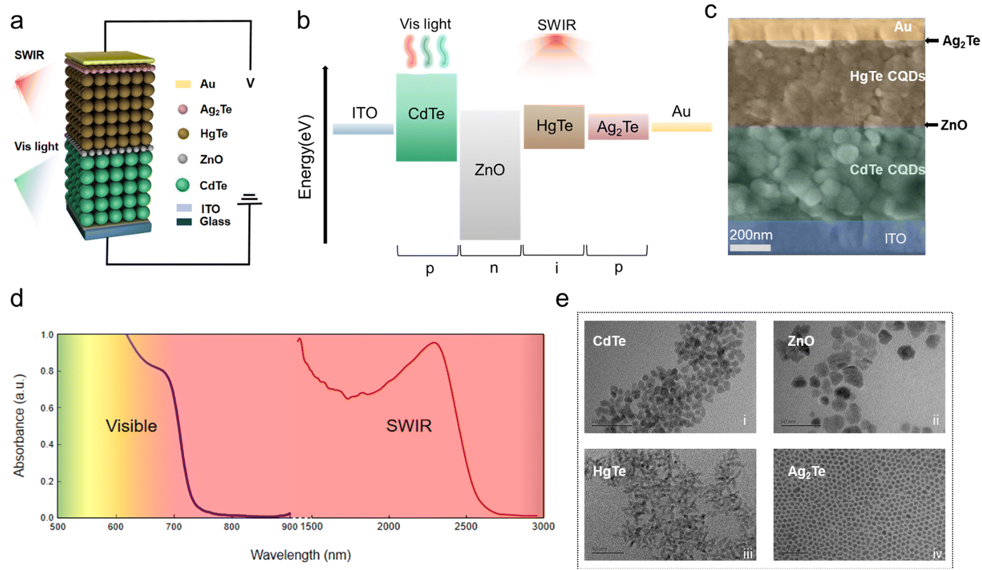 | ||
| Fig. 1 Architecture of the dual-band visible and SWIR photodetector. (a) Structure diagram of the dual-band device. (b) Energy band structure diagram of the dual-band device. (c) Cross-sectional SEM image of the dual-band device. (d) Absorption spectra of CdTe CQDs and HgTe CQDs. (e) TEM images of the CdTe, ZnO, HgTe, and Ag2Te materials. | ||
The absorption spectra of the CdTe CQDs and HgTe CQDs are shown in Fig. 1d. The cutoff wavelengths of the synthesized CdTe and HgTe CQDs are about 700 and 2300 nm, which are in the VIS and SWIR band range, respectively. Transmission electron microscopy (TEM) images of the CdTe, ZnO, HgTe, and Ag2Te materials are shown in Fig. 1e.
Characterization of the device performance
First, we fabricated CdTe and HgTe single-band devices. The fabrication process of the CdTe/ZnO single-band devices is presented in Supplement 2 (S2) (ESI†). The ligand exchange process with pyridine of the CdTe CQDs is essential for fabricating high-performance devices. The photocurrent of the CdTe single-band devices is increased by about ten times at zero bias after the ligand exchange process (Fig. S1, ESI†), which is attributed to the improved CdTe carrier mobility.38,39 The CdTe/ZnO single-band devices are capable of detecting visible light and exhibited an excellent performance under 700 nm visible light illumination with an optical power of 8.0 × 10⁻⁴ W cm−2 (Fig. 2a(i) and Fig. S2, ESI†). The detailed preparation steps of the ZnO/HgTe/Ag2Te single-band devices are shown in S3 (ESI†).40 With the presence of the ZnO layer, the rectifying characteristics of the devices are greatly enhanced compared with the HgTe CQDs photodiodes without ZnO, which is similar to previous studies (Fig. S3, ESI†).41 The dark current density of the ZnO/HgTe/Ag2Te devices is significantly reduced by nearly eight times (Fig. S3, ESI†). The ZnO/HgTe/Ag2Te single-band devices can detect SWIR with a cutoff wavelength of 2300 nm at room temperature, and under illumination with a calibrated 600 °C blackbody they demonstrate an excellent performance of 2.2 × 10⁻³ W cm−2 (Fig. 2a(ii) and Fig. S4, ESI†).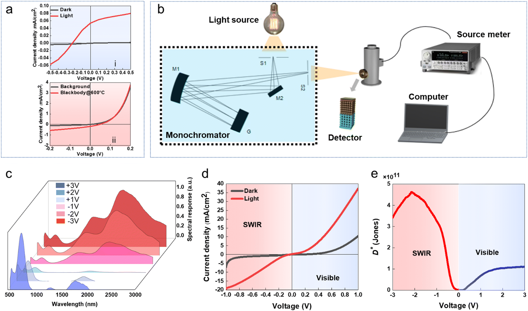 | ||
| Fig. 2 Performance of dual-band visible and SWIR photodetectors. (a) Current density–voltage curves of CdTe/ZnO single-band device and ZnO/HgTe/Ag2Te single-band device. (b) Illustration of the performance characterization system. (c) Response spectra of the dual-band device under positive and negative bias. (d) Current density–voltage curves of the dual-band device. (e) Specific detectivity of the dual-band device under positive and negative bias. | ||
The dual-band visible and SWIR detector arranged in a CdTe/ZnO/HgTe/Ag2Te back-to-back photodiode configuration were fabricated. The fabrication process is detailed in the Experimental section, and the CdTe also underwent ligand exchange. The bias-tunable spectral response curves of the dual-band devices were characterized using the measurement system illustrated in Fig. 2b. The detectors exhibit bias-dependent dual-band visible and SWIR spectral responses, as shown in Fig. 2c. By changing the bias voltage from −3 V to +3 V, the spectral response gradually switches from SWIR mode to visible mode. The response amplitude increases with the intensity of the bias voltage. Crosstalk signals exist, as shown in Fig. 2c and Fig. S5 (ESI†), but the magnitudes of these signals are tiny and can be ignored.
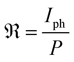
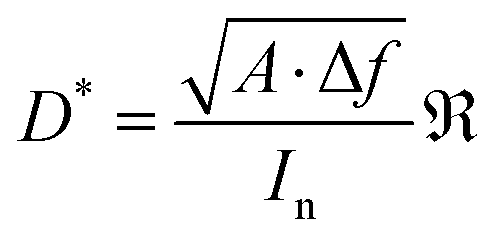
The current density–voltage curve of the dual-band detector using a tungsten lamp as the light source is shown in Fig. 2d. The black line is the dark current curve, and the dark current is suppressed for both positive and negative bias voltages due to the back-to-back diode structure. The red line presents the current density–voltage curve under illumination, and the dual-band detector exhibits a significant photocurrent at both positive and negative bias voltages. Both the responsivity ℜ and the specific detectivity D* are important indicators of a detector. The calculation process for the responsivity is as follows:
 | (1) |
 | (2) |
| Active materials | Wavelength (nm) | Voltage (V) | Incident light intensity (W cm−2) | Responsivity (A W−1) | Noise current (A Hz−1/2) | Detectivity (Jones) | Ref. |
|---|---|---|---|---|---|---|---|
| Ta2NiSe3/GaSe | 520/1550 | — | 1.4 × 10⁻⁸/3.0 × 10−8 | 4.8/0.15 | — | 1.1 × 10⁹ | 5 |
| SnO2/CsPbBr3 | 320/530 | 3/3 | — | 3.47 × 10⁻⁴/2.93 × 10−4 | — | 1.6 × 10¹⁰/1.2 × 1010 | 42 |
| N-InAsSb/N-GaSb | 1700/3400 | 0.3–0.8 | — | 0.3/40 | — | 1.5 × 10¹¹/1.4 × 109 | 43 |
| InP/InGaAs/GaAsSb | 1640/2000 | −0.1/−1 | — | 0.57/0.22 | — | 2.63 × 10¹¹/1.96 × 109 | 44 |
| MAPbI3 | 405/1064 | 1/0.01 | 3.31 × 10⁻²/3 × 10−2 | 680/1.74 | Noise equivalent power: 3.2 pW Hz−1/2/1.9 nW Hz−1/2 | 1.2 × 10⁹/5.4 × 107 | 15 |
| MAPbI3/IEICO | 650/820 | — | 5.6 × 10⁻³/5.6 × 10−3 | 0.28/0.14 | 4 × 10⁻¹⁴ | 1.45 × 10¹²/7.37 × 1011 | 3 |
| InSe/Au | 365/685 | 0 | 1.57 × 10⁻²/1.31 × 10−1 | 0.369/0.244 | — | 5 × 10¹²/1 × 1011 | 45 |
| ZnCdSe/ZnCdMgSe | 4800/7600 | 5/1 | — | 0.011/0.007 | ∼2 × 10⁻¹⁴/∼1 × 10−13 | 2 × 10⁸/2 × 107 | 47 |
| Ge/Si | 1000/1550 | 1/−0.5 | 10−6–10−2/10−5–10−1 | 0.33/0.63 | — | 7 × 10¹¹/2 × 1010 | 6 |
| Cs3Cu2I5/PdTe2/Ge | 265/1550 | — | 6.8 × 10⁻⁵/8.0 × 10−5 | 0.0257/0.6941 (0 V) | 1.01 × 10⁻¹² (0 V) | 5.08 × 10⁹/1.37 × 1011 (0 V) | 46 |
| 0.3629/0.6984 (−0.1 V) | 4.2 × 10⁻¹⁰ (−0.1 V) | 1.73 × 10⁸/3.33 × 108 (−0.1 V) | |||||
| 0.5758/0.7031 (−0.2 V) | 4.3 × 10⁻¹⁰ (−0.2 V) | 1.83 × 10⁸/2.23 × 108 (−0.2 V) | |||||
| 0.7442/0.7072 (−0.3 V) | 7.8 × 10⁻¹⁰ (−0.3 V) | 1.91 × 10⁸/1.81 × 108 (−0.3 V) | |||||
| 0.7325/0.7125 (−0.4 V) | |||||||
| CdTe/ZnO/HgTe | 700/2100 | 3/−2 | 8.0 × 10⁻⁴/2.2 × 10−3 | 0.5/0.9 (1.1 at −3 V) | 5 × 10⁻¹³/3 × 10−13 | 1.1 × 10¹¹/4.5 × 1011 | This work |
Device simulation
To investigate the physics and working mechanism of the dual-band device, finite element analysis was carried out using the wave optical module and the semiconductor module. The structure diagram of the simulation model is shown in Fig. 3a. The CdTe (400 nm), ZnO (50 nm), and HgTe (400 nm) are superimposed vertically, and the periodic boundary condition is used.48 Bulk CdTe has a bandgap of 1.45 eV.49,50 Besides, bulk HgTe possesses a zero gap in theory.51 The CQDs have different energy levels in their bulk forms. In our simulation, the energy bandgaps of the CdTe CQDs and the HgTe CQDs are 1.5 and 0.45 eV, respectively.52–60 The refractive index of the CQD film is 2.3 + 0.1i.61,62 Besides, the energy bandgap of ZnO is 3.3 eV in the simulation.52–56 Layers of p-type Ag2Te and n-type ZnO are introduced at the top of HgTe and at the interface between HgTe and CdTe, respectively. Fig. 3b shows the doping concentration distribution of the dual-band devices. The simulated spectral response of the dual-band detector under different polarity bias voltages is shown in Fig. 3c. The device exhibits an obvious visible band response under a positive bias and an SWIR response under a negative bias, similar to the experimental results (Fig. 2c).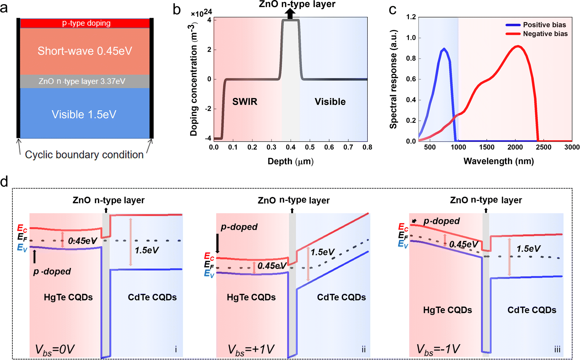 | ||
| Fig. 3 Simulation of the dual-band visible and SWIR photodetector. (a) Simulation model structure of the dual-band device. (b) Distribution of the doping concentration. (c) Simulated spectral responses of the dual-band device under negative and positive bias voltages. (d) Simulated energy band diagram of the dual-band device under zero (i), positive (ii), and negative (iii) bias voltages. | ||
To understand the bias-switchable spectral response of the dual-band visible and SWIR PD, the energy band structure of the devices at zero, positive and negative bias voltages was simulated and analyzed (Fig. 3d). Under a positive bias, the visible CdTe/ZnO heterojunction is in the reverse working region. The CdTe CQD layer generates electron–hole pairs under visible light, and electrons and holes are transferred to the adjacent ZnO layer and the ITO electrode, respectively. The ZnO layer is beneficial for fast electron transport. More importantly, a large band-edge offset between the ZnO layer and the CdTe layer prevents hole injection into the HgTe layer. Only the CdTe visible-light-absorbing layer generates photogenerated carriers under a positive bias, inducing CdTe band bending. Under a negative bias, the SWIR ZnO/HgTe/Ag2Te heterojunction begins to operate in the reverse region. The Fermi level near the HgTe/Ag2Te interface tends to the valence band due to the introduction of p-type Ag2Te doping, resulting in a lower energy barrier for hole transport. The photogenerated charges are selectively extracted from the HgTe CQD layer due to the hole barrier effect of the ZnO layer. The energy bend of the HgTe layer is bent, caused by the high density of SWIR light-generated carriers. The above mechanism enables the detector to effectively access two separate visible and SWIR channels through simple bias regulation.
Dual-band imaging
The visible and SWIR dual-mode imaging of the detector is demonstrated using a single-pixel scanning imaging system with a tungsten lamp as the light source (Fig. 4a). As the projected image is scanned by the detector, the photocurrent is amplified by the amplifier and recorded by the high-speed acquisition card. The four different chemical solvents, of water, IPA, toluene, and methanol (MeOH), in the glass vials are the imaging objects, as shown in Fig. 4b(i). Under a positive bias, the dual-band detector operates in the visible mode. The gap between the current signals at the baseline of the same height is hardly noticeable (Fig. 4b(ii)). All liquids are transparent, and the liquid height is difficult to determine (Fig. 4b(ii)). The dual-band detector changes to the SWIR mode under a negative bias. Transparent objects in visible light can be identified in the SWIR range due to their different vibrational absorptions. As expected, there are significantly different current signals at the baseline of the same height for various chemical solvents, causing the transparent solvents in visible mode to appear differently in the SWIR mode (Fig. 4b(iii)). Besides, a soldering iron held behind the silicon wafer cannot be seen in the visible mode of the dual-band detector under a positive bias, as shown in Fig. 4c(ii). However, the soldering iron that is blocked by silicon wafer can be clearly captured by the dual-band detector when under a negative bias, indicating that the device operates in the SWIR mode (Fig. 4c(iii)).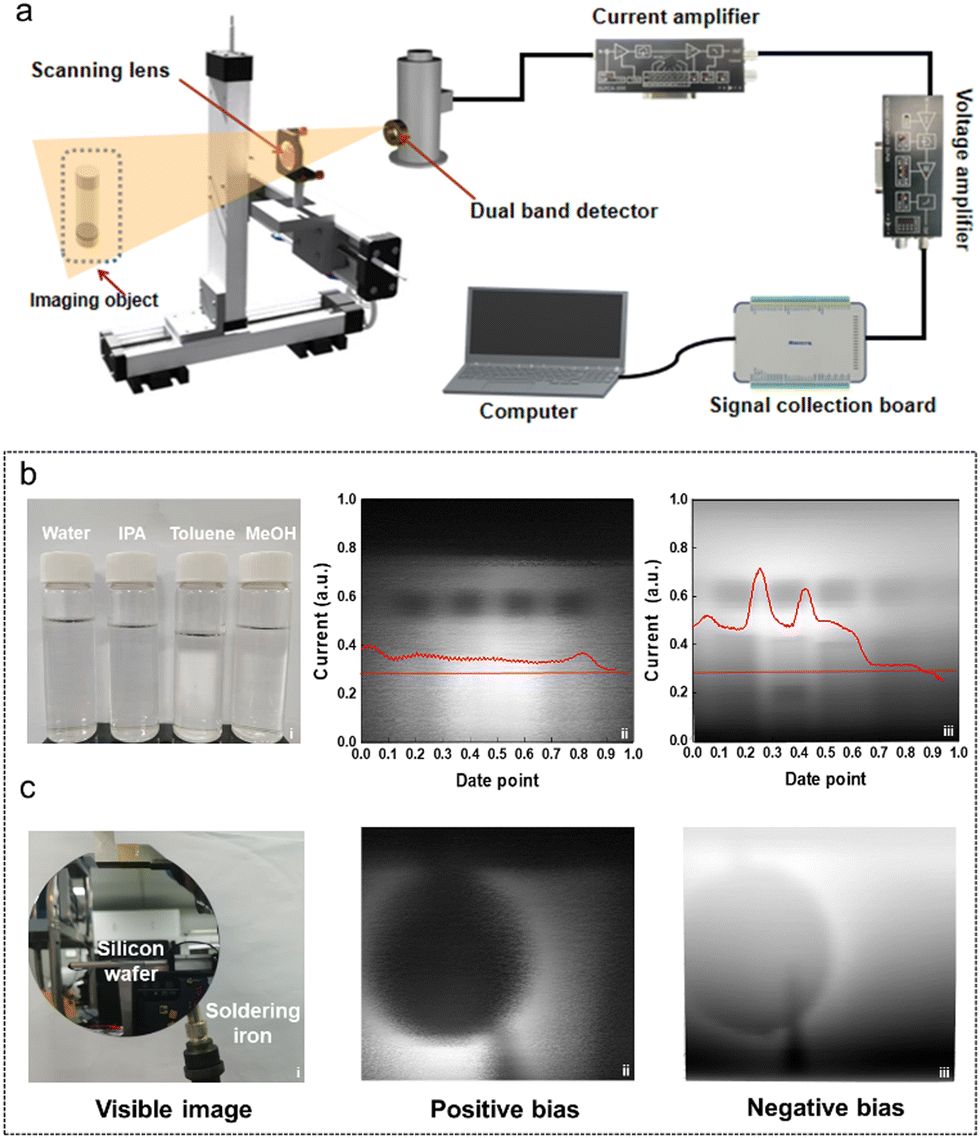 | ||
| Fig. 4 Dual-band imaging. (a) Illustration of the single-pixel scanning imaging setup. (b) and (c) Visible images (i) and the images captured by the dual-band detector under positive (ii) and negative (iii) bias voltages for (b) four different chemical solvents in glass vials and (c) a silicon wafer and soldering iron arrangement. | ||
The dual-band detector operating in the visible and SWIR modes under positive and negative bias voltages, respectively, are verified by the imaging results. When a positive voltage is applied, the visible CdTe/ZnO heterojunction is in the reverse bias and the visible channel begins to operate. The ZnO layer serves as both an electron-transporting layer and a hole-blocking layer, which not only promotes electron transport in the visible channel but also inhibits hole injection from the visible to the SWIR absorbing layer. When the device is operated under a negative bias, the SWIR ZnO/HgTe/Ag2Te heterojunction begins to operate in the reverse region. Similarly, the large band-edge offset between the ZnO layer and the HgTe layer enables the dual-band device to respond only to SWIR light. Thus, the detector realizes visible and SWIR dual-mode imaging through changing the bias polarity, providing more information about detected objects than is achievable from single-band images.
Conclusions
In this work, we constructed a metal chalcogenide CdTe/HgTe CQD-based dual-band detector consisting of two stacked photodiodes, which realizes bias-controlled visible and SWIR dual-operation modes. An n-type ZnO layer is introduced between the VIS CdTe and SWIR HgTe layers as both an electron-transporting layer and a hole-blocking layer to prevent the injection of holes from one sensor layer to the other. The working mechanism of the dual-band PD is investigated through simulations. With the well-designed architecture, the dual-band device can switch between visible and SWIR modes by changing the polarity and the magnitude of the bias. The response peaks of the device are at 700 and 2100 nm in the visible and SWIR modes, respectively. The performance of the dual-band device is excellent, with a low noise current of about 10−13 A Hz−1/2, high responsivity values of 0.5 A W−1 (VIS) and 1.1 A W−1 (SWIR), and a high detectivity above 1011 Jones both in the visible and SWIR modes at room temperature. VIS/SWIR dual-band imaging is demonstrated, providing more comprehensive object information than is achievable using single-band PDs. The obtained high-performance dual-band visible and SWIR detector offers the potential for more applications, such as autonomous driving, biomedicine, computer surveillance, and military operations.Author contributions
The manuscript was written through the contributions of all authors. All authors have approved the final version of the manuscript.Conflicts of interest
There are no conflicts to declare.Acknowledgements
This work was funded by the National Key R&D Program of China (2021YFA0717600), the National Natural Science Foundation of China (NSFC No. 62035004 and NSFC No. 62105022) and the China Postdoctoral Science Foundation (2022M710396). X.T. is sponsored by the Young Elite Scientists Sponsorship Program by CAST (No. YESS20200163).References
- Z. Lan, Y. Lei, W. K. E. Chan, S. Chen, D. Luo and F. Zhu, Sci. Adv., 2020, 6, 1–10 CrossRef PubMed.
- J. Zhao, X. Wang, Y. Xu, Y. Pan, Y. Li, J. Chen, Q. Li, X. Zhang, Z. Zhu, Z. Zhao, E. E. Elemike, D. C. Onwudiwe, B. S. Bae, S. Bin Shafie and W. Lei, ACS Appl. Mater. Interfaces, 2022, 14, 25824–25833 CrossRef CAS PubMed.
- C. Li, J. Lu, Y. Zhao, L. Sun, G. Wang, Y. Ma, S. Zhang, J. Zhou, L. Shen and W. Huang, Small, 2019, 15, 1–10 Search PubMed.
- S. Zhang, G. Mu, J. Cao, Y. Luo, Q. Hao, M. Chen, Y. Tan, P. Zhao and X. Tang, Photonics Res., 2022, 10, 1987–1995 CrossRef CAS.
- Y. Zhang, L. Huang, J. Li, Z. Dong, Q. Yu, T. Lei, C. Chen, L. Yang, Y. Dai, J. Zhang, W. Yu, Q. Bao and K. Zhang, Appl. Phys. Lett., 2022, 120, 261101 CrossRef CAS.
- E. T. Simola, A. De Iacovo, J. Frigerio, A. Ballabio, A. Fabbri, G. Isella and L. Colace, Opt. Express, 2019, 27, 8529 CrossRef CAS PubMed.
- L. Li, H. Chen, Z. Fang, X. Meng, C. Zuo, M. Lv, Y. Tian, Y. Fang, Z. Xiao, C. Shan, Z. Xiao, Z. Jin, G. Shen, L. Shen and L. Ding, Adv. Mater., 2020, 32, 1–9 Search PubMed.
- X. Tang, M. M. Ackerman, M. Chen and P. Guyot-Sionnest, Nat. Photonics, 2019, 13, 277–282 CrossRef CAS.
- Y. Li, Z. Shi, W. Liang, L. Wang, S. Li, F. Zhang, Z. Ma, Y. Wang, Y. Tian, D. Wu, X. Li, Y. Zhang, C. Shan and X. Fang, Mater. Horiz., 2020, 7, 530–540 RSC.
- X. Xu, W. Deng, X. Zhang, L. Huang, W. Wang, R. Jia, D. Wu, X. Zhang, J. Jie and S. T. Lee, ACS Nano, 2019, 13, 5910–5919 CrossRef CAS PubMed.
- D. Shen, Z. Guan, M. Li, S. W. Tsang, W. Zhang, M. F. Lo and C. S. Lee, J. Mater. Chem. C, 2021, 9, 3814–3819 RSC.
- Y. Wang, B. Siegmund, Z. Tang, Z. Ma, J. Kublitski, S. Xing, V. C. Nikolis, S. Ullbrich, Y. Li, J. Benduhn, D. Spoltore, K. Vandewal and K. Leo, Adv. Opt. Mater., 2021, 9, 1–8 RSC.
- B. Huang, J. Liu, Z. Han, Y. Gu, D. Yu, X. Xu and Y. Zou, ACS Appl. Mater. Interfaces, 2020, 12, 48765–48772 CrossRef CAS PubMed.
- C. Li, H. Wang, F. Wang, T. Li, M. Xu, H. Wang, Z. Wang, X. Zhan, W. Hu and L. Shen, Light: Sci. Appl., 2020, 9, 31 CrossRef CAS PubMed.
- Y. Li, Y. Zhang, T. Li, M. Li, Z. Chen, Q. Li, H. Zhao, Q. Sheng, W. Shi and J. Yao, Nano Lett., 2020, 20, 5646–5654 CrossRef CAS PubMed.
- H. Kim, W. Kim, Y. Pak, T. J. Yoo, H. W. Lee, B. H. Lee, S. Kwon and G. Y. Jung, Laser Photonics Rev., 2020, 14, 1–7 Search PubMed.
- A. Imran, M. Sulaman, S. Yang, A. Bukhtiar, M. Qasim, S. Elshahat, M. S. A. Khan, G. Dastgeer, B. Zou and M. Yousaf, Surf. Interfaces, 2022, 29, 101772 CrossRef CAS.
- S. Das, D. Pandey, J. Thomas and T. Roy, Adv. Mater., 2019, 31, 1–35 Search PubMed.
- A. Imran, M. Sulaman, M. Yousaf, M. A. Anwar, M. Qasim, G. Dastgeer, K. A. A. Min-Dianey, B. Wang and X. Wang, Adv. Mater. Interfaces, 2022, 2200105 CrossRef.
- C. Li, J. Lu, Y. Zhao, L. Sun, G. Wang, Y. Ma, S. Zhang, J. Zhou, L. Shen and W. Huang, Small, 2019, 15, 1–10 Search PubMed.
- S. Bhowmick, R. Sen, C. P. Saini, R. Singhal, L. Walczak, M. Gupta, D. M. Phase and A. Kanjilal, J. Phys. Chem. C, 2021, 125, 4846–4859 CrossRef CAS.
- G. Konstantatos and E. H. Sargent, Nat. Nanotechnol., 2010, 5, 391–400 CrossRef CAS PubMed.
- M. V. Kovalenko, Nat. Nanotechnol., 2015, 10, 994–997 CrossRef CAS PubMed.
- S. Keuleyan, E. Lhuillier and P. Guyot-Sionnest, J. Am. Chem. Soc., 2011, 133, 16422–16424 CrossRef CAS PubMed.
- P. Zhao, G. Mu, M. Chen and X. Tang, Coatings, 2022, 12, 499 CrossRef CAS.
- Y. Luo, S. Zhang, X. Tang and M. Chen, J. Mater. Chem. C, 2022, 10, 8218–8225 RSC.
- A. Imran, J. Jiang, D. Eric, M. N. Zahid, M. Yousaf, M. Ahmad and S. A. Hassan, Results Phys., 2018, 10, 241–247 CrossRef.
- A. Imran, M. Sulaman, Y. Song, D. Eric, M. N. Zahid, M. Yousaf, M. I. Saleem, M. Li and D. Li, J. Comput. Electron., 2021, 20, 310–316 CrossRef CAS.
- S. G. Kumar and K. S. R. K. Rao, Energy. Environ. Sci., 2014, 7, 45–102 RSC.
- X. Y. Yu, B. X. Lei, D. Bin Kuang and C. Y. Su, Chem. Sci., 2011, 2, 1396–1400 RSC.
- F. D. De Menezes, A. G. Brasil, W. L. Moreira, L. C. Barbosa, C. L. Cesar, R. D. C. Ferreira, P. M. A. De Farias and B. S. Santos, Microelectron. J., 2005, 36, 989–991 CrossRef CAS.
- X. Tang and K. W. C. Lai, ACS Appl. Nano Mater., 2019, 2, 6701–6706 CrossRef CAS.
- M. Chen, X. Lan, X. Tang, Y. Wang, M. H. Hudson, D. V. Talapin and P. Guyot-Sionnest, ACS Photonics, 2019, 6, 2358–2365 CrossRef CAS.
- M. M. Ackerman, X. Tang and P. Guyot-Sionnest, ACS Nano, 2018, 12, 7264–7271 CrossRef CAS PubMed.
- X. Tang and K. W. C. Lai, in 2016 IEEE 16th International Conference on Nanotechnology (IEEE-NANO), IEEE, 2016, pp. 494–497.
- M. Chen and P. Guyot-Sionnest, ACS Nano, 2017, 11, 4165–4173 CrossRef CAS PubMed.
- M. G. Panthani, J. M. Kurley, R. W. Crisp, T. C. Dietz, T. Ezzyat, J. M. Luther and D. V. Talapin, Nano Lett., 2014, 14, 670–675 CrossRef CAS PubMed.
- C. Livache, B. Martinez, N. Goubet, J. Ramade and E. Lhuillier, Front. Chem., 2018, 6 DOI:10.3389/fchem.2018.00575.
- J. Jasieniak, B. I. MacDonald, S. E. Watkins and P. Mulvaney, Nano Lett., 2011, 11, 2856–2864 CrossRef CAS PubMed.
- S. Keuleyan, E. Lhuillier, V. Brajuskovic and P. Guyot-Sionnest, Nat. Photonics, 2011, 5, 489–493 CrossRef CAS.
- G. Mu, T. Rao, S. Zhang, C. Wen, M. Chen, Q. Hao and X. Tang, ACS Appl. Mater. Interfaces, 2022, 14, 45553–45561 CrossRef CAS PubMed.
- Y. Zhang, W. Xu, X. Xu, J. Cai, W. Yang and X. Fang, J. Phys. Chem. Lett., 2019, 10, 836–841 CrossRef CAS PubMed.
- J. Tong, L. Y. M. Tobing, Y. Luo, D. Zhang and D. H. Zhang, Sci. Rep., 2018, 8, 1–9 CAS.
- Z. Xie, Z. Deng, X. Zou and B. Chen, IEEE Photonics Technol. Lett., 2020, 32, 1003–1006 CAS.
- M. Dai, H. Chen, R. Feng, W. Feng, Y. Hu, H. Yang, G. Liu, X. Chen, J. Zhang, C. Y. Xu and P. Hu, ACS Nano, 2018, 12, 8739–8747 CrossRef CAS PubMed.
- Y. Liang, C. Xie, C. Y. Dong, X. W. Tong, W. H. Yang, C. Y. Wu and L. B. Luo, J. Mater. Chem. C, 2021, 9, 14897–14907 RSC.
- Y. Kaya, A. Ravikumar, G. Chen, M. C. Tamargo, A. Shen and C. Gmachl, AIP Adv., 2018, 8, 075105 CrossRef.
- P. Zhao, G. Mu, M. Chen and X. Tang, Coatings, 2022, 12, 499 CrossRef CAS.
- B. I. MacDonald, A. Martucci, S. Rubanov, S. E. Watkins, P. Mulvaney and J. J. Jasieniak, ACS Nano, 2012, 6, 5995–6004 CrossRef CAS PubMed.
- G. Jain, A. Ahnood, A. Chanaewa, K. Fox and P. Mulvaney, Phys. Lett. A, 2019, 383, 1199–1202 CrossRef CAS.
- X. Shen, J. C. Peterson and P. Guyot-Sionnest, ACS Nano, 2022, 16, 7301–7308 CrossRef CAS PubMed.
- J. Jasieniak, B. I. MacDonald, S. E. Watkins and P. Mulvaney, Nano Lett., 2011, 11, 2856–2864 CrossRef CAS PubMed.
- H. Liu, Y. Tian, Y. Zhang, K. Gao, K. Lu, R. Wu, D. Qin, H. Wu, Z. Peng, L. Hou and W. Huang, J. Mater. Chem. C, 2015, 3, 4227–4234 RSC.
- X. Guo, Q. Tan, S. Liu, D. Qin, Y. Mo, L. Hou, A. Liu, H. Wu and Y. Ma, Nano Energy, 2018, 46, 150–157 CrossRef CAS.
- B. Chen, J. Liu, Z. Cai, A. Xu, X. Liu, Z. Rong, D. Qin, W. Xu, L. Hou and Q. Liang, Nanomaterials, 2019, 9, 626 CrossRef CAS PubMed.
- M. Hou, Z. Zhou, A. Xu, K. Xiao, J. Li, D. Qin, W. Xu and L. Hou, Nanomaterials, 2021, 11, 2071 CrossRef CAS PubMed.
- A. Jagtap, B. Martinez, N. Goubet, A. Chu, C. Livache, C. Gréboval, J. Ramade, D. Amelot, P. Trousset, A. Triboulin, S. Ithurria, M. G. Silly, B. Dubertret and E. Lhuillier, ACS Photonics, 2018, 5, 4569–4576 CrossRef CAS.
- U. N. Noumbé, C. Gréboval, C. Livache, A. Chu, H. Majjad, L. E. Parra López, L. D. N. Mouafo, B. Doudin, S. Berciaud, J. Chaste, A. Ouerghi, E. Lhuillier and J. F. Dayen, ACS Nano, 2020, 14, 4567–4576 CrossRef PubMed.
- M. M. Ackerman, M. Chen and P. Guyot-Sionnest, Appl. Phys. Lett., 2020, 116, 083502 CrossRef CAS.
- E. Lhuillier, S. Keuleyan, P. Zolotavin and P. Guyot-Sionnest, Adv. Mater., 2013, 25, 137–141 CrossRef CAS PubMed.
- X. Tang, M. M. Ackerman and P. Guyot-Sionnest, ACS Nano, 2018, 12, 7362–7370 CrossRef CAS PubMed.
- Y. Ning, S. Zhang, Y. Hu, Q. Hao and X. Tang, Coatings, 2020, 10, 1–8 CrossRef.
Footnotes |
| † Electronic supplementary information (ESI) available: Materials, the fabrication process of CdTe and HgTe single-band devices, the effect of the ligand exchange process for CdTe single-band devices, the effect of the ZnO layer for HgTe single-band devices, the response spectra of CdTe and HgTe single-band devices and dual-band devices. See DOI: https://doi.org/10.1039/d3tc00066d |
| ‡ These authors contributed equally to this work. |
| This journal is © The Royal Society of Chemistry 2023 |